All posts by Axel

http://www.geekdot.com/about-me/

Fixing the Quadra 950 power-supply

One day the power-supply of my beloved Quadra went “bzzzzzt-poof” (sparks flying, smoke rising).
First I was desperate… try to find a Quadra 950 power-supply these days. And if you find one, it’ll cost you the same you’d pay for a complete system… and then you’re still not sure, if it won’t go poof very soon, too.

Then I thought: Hey, why don’t replace the whole thing by something more modern, much cheaper and smaller?!
It’s already been proven with other Mac systems that using a standard PC power-supply (PSU for short) is feasible, so why should a Quadra 950 power-supply be much different?
As there are some descriptions out there – mainly for those “10-pin connectors” (Mac IIcx, vx or PMac family) I thought it might be helpful to have a step-by-step how-to with lots of photos…

We’re interuppting this transmission for a stern word of warning:

Working on/in power supplies is dangerous. I take no responsibility for any damages, injuries or fatal strokes! If you’re unsure if you can do this hack, just don’t do it!

First (obviously), unplug the unit. Leave it unplugged for 15 minutes or so. In most PSUs there are bleeder resistors that will bleed down the stored voltages inside over time BUT THERE ARE NO GUARANTEES!!

When you open the unit, understand that there are two hazards:

  1. Stored high voltage (200V or so) on the “input” side of the unit.
  2. Stored high currents (tens of amps) on the “output” side of the unit.

Either 1 or 2 can be deadly. If you die, it’s social darwinism. You have been warned. 

Dismantle

So for the initial try I pulled a cheap ATX power-supply out of my junk-pile (wife-speak for “basement”) and put it next to the original, humongous Supplyzilla created by Apple. Ok, that should fit in 😉
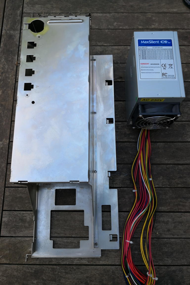
Opening Supplyzilla is another thing. About 10 screws, a cut in my finger and 30 mins of cursing later I found the reason why I wasn’t able to get the two case-parts apart: Don’t forget to unplug the fan cable :-/
After this you can fold-open the case and have a good view onto huge capacitors, lots of dirt and 1990s tech…
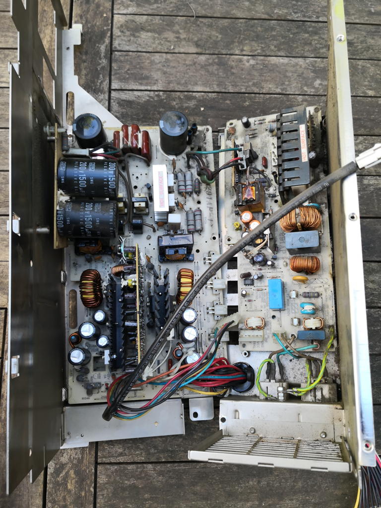
There are two PCBs each mounted to a side of the case. Unscrew and separate them – because mine was dead anyhow (and I wasn’t planning to repair it) separation was easy. Snip!
I wasn’t able to get the external cable-harness leading out of the case. So this was a 2nd snip-snap… I planned to use the original PC cables anyhow. You can reuse the original plug or use the one from the ATX PSU (if it’s a 24pin one).
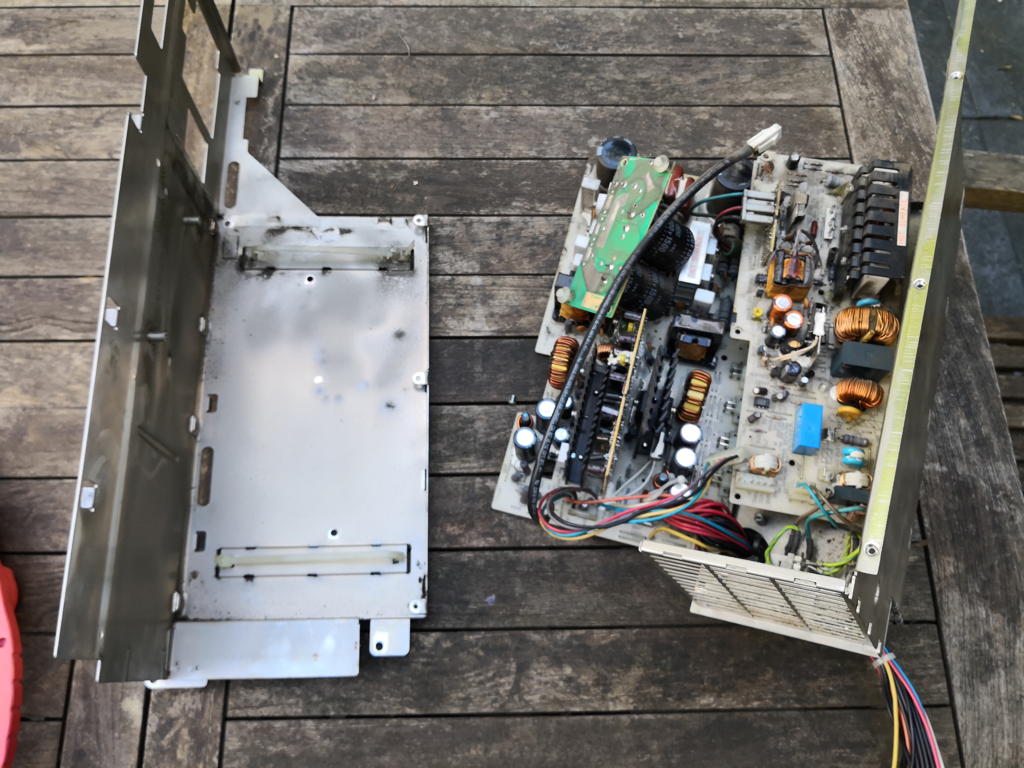
Here they are… rest in pieces 😛
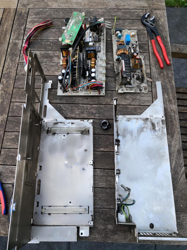
Fitting room

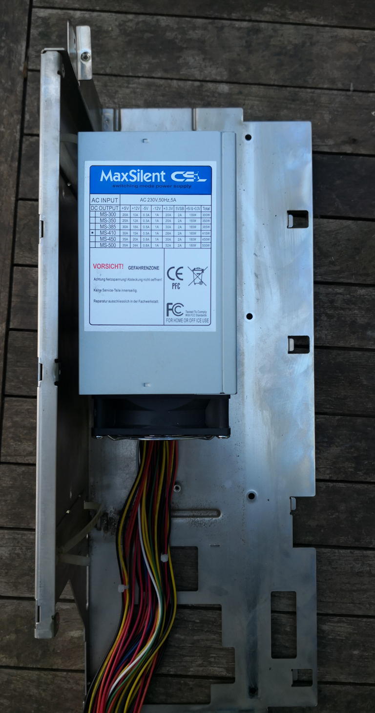
Next up: The first fitting… even still in its enclosure it would nearly fit two times.
BTW: I like the sticker saying in German “VORSICHT! GEFAHRENZONE!” (Caution, danger-zone!) That’s soooo 80’s Top-Gun 😀
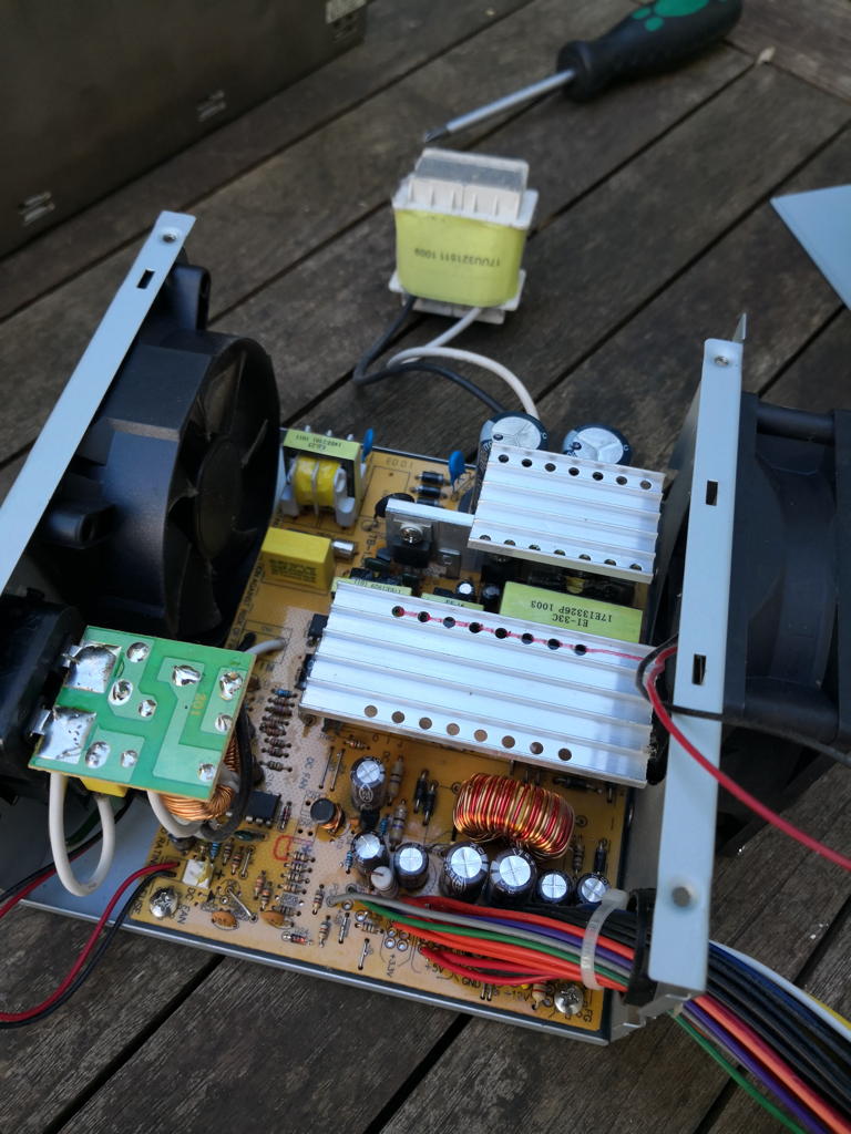
Because we have to modify the ATX PSU, it had to be stripped down, too. Compared to Supplyzilla it’s pretty deserted in there…
Yes, it’s a cheapo one looking at the passive PFC and could have be designed much better, but for the 1st try it’s OK.
2nd fitting making sure all heatsinks are well placed into the airflow, cables close to outlets (the fan will be replaced by a big one, of course).
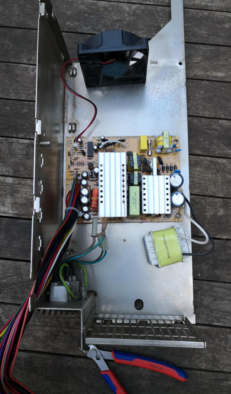
You will be assimilated…

Next step was a meditational one. Loosening all 24 pins clamped into the ATX plug. I used the “cut staple method”. One to the left, one to the right, push them in, pull the cable… repeat.
Configuration of the Q950 plug will be described further down. I suggest to do this as one of the last steps. For now just tape all loosened pins together to save them from bending.
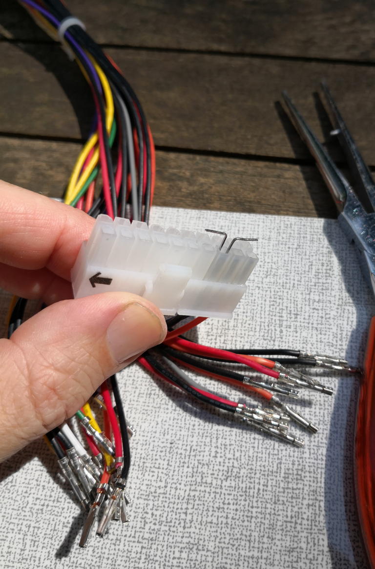
Having the preparations done, it was on to the workshop drilling some holes and cutting screw threads (optional but nicer than holes and nuts)…
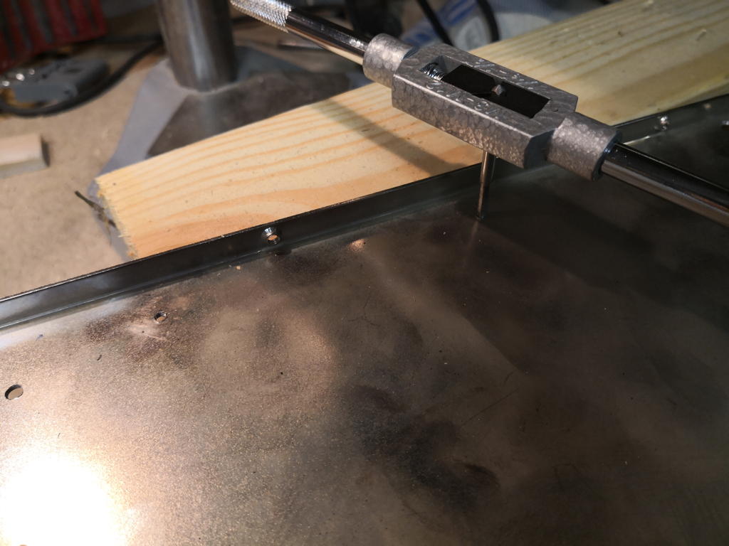
…to have a proper seating for the stand-offs. We don’t want the PCB touch the case, don’t we?
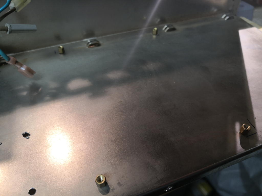
All fits nicely. The PFC screwed to the case like in its original habitat – ugly, but will do for now.
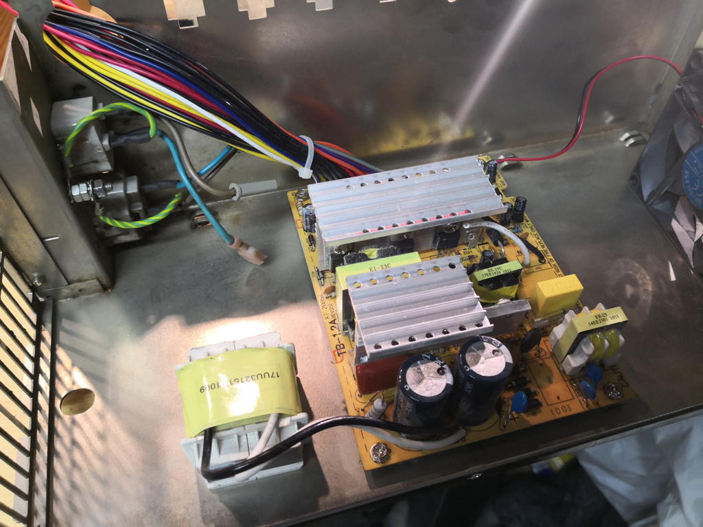
The noise filter was directly soldered to the power-out plug. Again ugly, unprofessional but OK for a try.
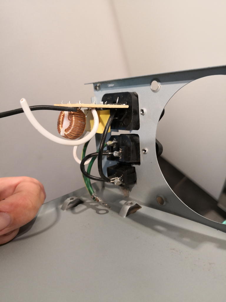
So the filter went into the case and unneeded cables like 3V, were shortended and kept inside the power-supply.

Connecting the dots

Now for the plug-configuration. All documentation I’ve found on the web were wrong – dead-wrong, even leading to drama
So this is the correct pinout for Quadra 900/950’s:
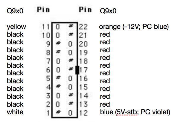
Having this, the mapping from the “Mac-plug” to your ATX-PSUs cables is pretty straightforward:

  • Red (5 volts) stays red
  • Black (Ground) stays black
  • Yellow (+12V) also stays that way, too
  • Orange (-12) is blue in your ATX-PSU
  • Blue (5V standby) is the violet cable in ATX-PSUs
  • White is mostly unused on ATX-PSUs – we will recycle that cable for PFW…

As for 5V/GND wires don’t worry if your ATX PSU doesn’t offer enough of them (10 each). Mine just had five 5V wires, so I populated every 2nd slot in the plug.

Killing me softly

Finally the ‘circuit’ for using the Quadras soft-power feature had to be implemented – a simple rocker-switch connecting the green (Pwr_on) wire to GND would do, but this is just so below the mighty Quadras grandeur.
I opted for the very simple, more reasonable solution using a NPN-resistor… even a 74LS04 is an overkill in this case. Just my 2ct, though.

This is the schematic, nothing spectacular:
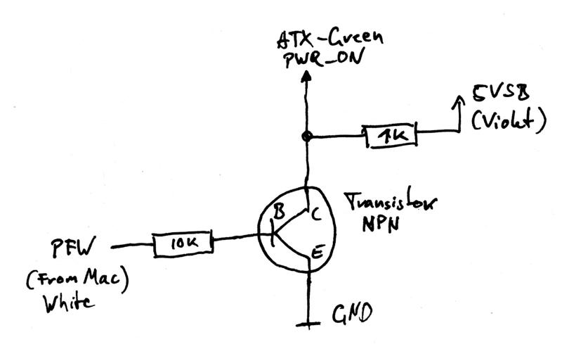
Yeah, the symbols for the resistors are European, that’s because… well, I am European 😉 As for the transistor use any NPN you can get easily. E.g. BC547 or BC549 (again, European numbering scheme, you’ll have to figure out JEDEC names if needed).

And here’s the PSU before its going to be closed and put back into my Q950.
Pink box: The soft-power ‘circuit’ (yeah, I was too lazy to create a PCB for a transistor and two resistors).
Green box: Unneeded cables been cut (3V, extra 12V, pwr_good).
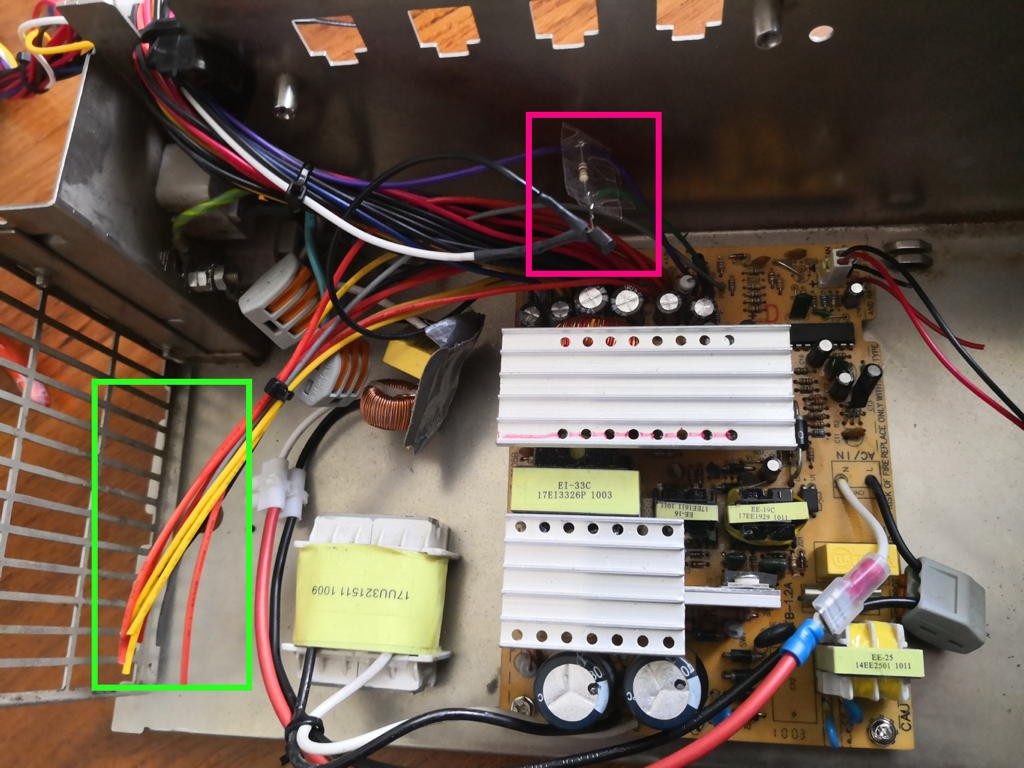
Everything else was routed outside (All 5V/GND, +12V, -12V, 5V_tickle and the white cable was cut and reused for PFW.

Hints: DON’T use the GND from fan-connectors! They might be modulated to control the fan speed and other wired things. Better use one of the e.g. unused 12V cable-pairs.
Check everything before closing the case – Again CAUTION!!! High voltage. You touch, you die!!

Woo-hoo! Lady Quadra works again!

Outlook

That was a cheap fix… about $5 in parts if you have to buy a used ATX PSU. To make things easier and look more professional I plan to design a small PCB which fits right where one of the original PSU PCBs sat, providing the 4 drive connectors (4-pin) so that you can keep using the original drive power-cables. Also I plan to add:

  • the soft-power circuit
  • a temperature fan speed controller
  • (optional) internal 5¼” power-connectors for solder-free connection to the external 4pin connectors.
Nothing happening in 2018?

Hey Axel, what’s up? No new post for months… are you still alive?

Yes, shame on me… it’s been really silent the last months. But that does not necessarily mean I’m not working on something.
Actually I was pulled into a 68k Apple Macintosh vortex which really got be big time. As you probably know I have a soft spot for all things 68000 and was a Mac user from day one (well, ~1985). User means that even I did not own one until 1994 (i.e. paying for it with own money) I borrowed, worked, sat in front of many models…

Long story short: Got my hands onto a SE/30, pulled an 040 accelerator from the basement, learned that it will never work in there… got lit 😉 Bought a IIci for checking and from there it went on uncontrolled… So the challenge is on to get this IIci accelerator working in sweet lil’ SE/30. Read the thread here (68kmla.org forum).

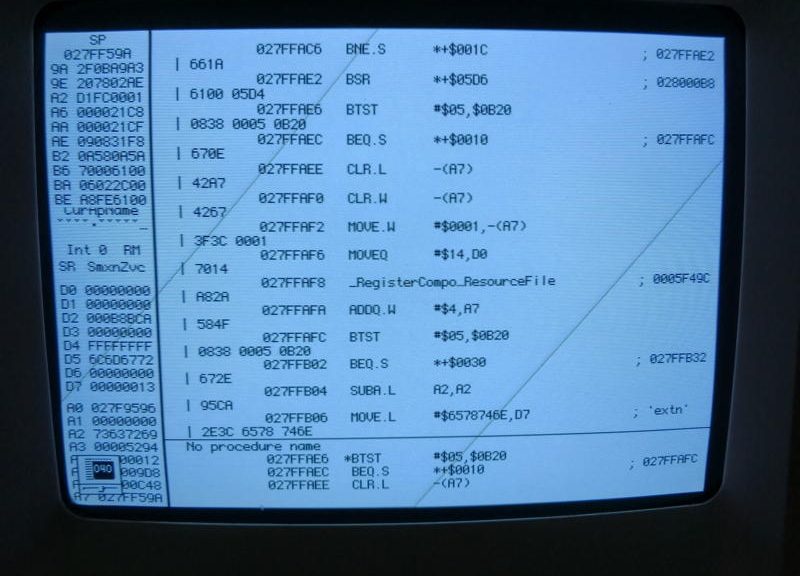
While I was a Mac user, I never went real deep into programming them. So here I am, digging through 6098 lines of disassembly and learn ‘new’ things like A5-world, Mac boot processes, the dirtiest tricks in MacsBug, INITs, how control panels work and last but not least patching Toolbox calls from the machine language side of things. It’s a steep learning curve, a total waste of time & energy. And I love it!

P.S.: I’ll write down the whole stunt into a post one day. But for now it’s totally work-in-progress… It’s done. Read the whole thing here. (There are 4 chapters)

TIGA programming

After we talked about the basics of the TIGA standard in the previous post, we’re now  trying to do some TIGA programming… (mind the absence of the word “useful”  😉 )

I can’t stress this enough: Compared to even the earliest 3D accelerators TIGA wasn’t fast. Actually it’s not meant to be a 3D accelerator at all, it’s a 2D accelerator which tried to cope with the slow ISA bus speed. With the arrival of VL-bus and then PCI, TIGA hadn’t had a chance – even with a TMS34082 FPU it reached a max of  160,000 polygons/sec and 25,000 shaded polygons/sec – and there’s no real support for textures. Fun fact: An original PlayStation (1, that is) did 180,000 textured and lighted polygons/sec…
Ah, and before you ask: No, there was no native Linux X11 support ever. There were two X11 servers: MetroLink offered a “stub” which translated X-call on the host to TIGA which ran on the card. And there was a DOS(!) X11 server from AGE Logic. That one ran solely inside the cards RAM, ignored TIGA completely and its speed was comparable to a Sparc 1 or Personal Iris  😕 The upside was, that was also the case on a slow i386/25 which was still usable running several tasks. So a lot of work was offloaded to the TMS340… OTOH you could invest that money in a i486 and a simple ET4000 to get the same responsiveness and got more CPU-Ooomp on top.

Demos

Anyhow, to have a quick start in TIGA programming, let’s do some demos… but before we start, make sure you can tick every point on this list:

  • You’ll need a running DOS (>= v3.2) system
  • Obviously a TIGA graphics card in an (E)ISA slot – VMs won’t take you far here.
  • A successfully loaded CD and GM (what’s that? Read the 1st TIGA post over here!)
  • A decent C compiler – I use Borland C (Turbo C v2 is fine, too) for that
  • The API documentation PDF from TI (aka “Interface Users Guide”)

…and the libraries. Those came in the so-called DDK (Drive Development Kit, download it here), which was meant to develop drivers on the DOS side of things but can also be used to write some code making use of the insane TMS340 powers 😉
This DDK contains some (thin) documentation of how to set-up your compiler and the important libraries as well as the include files.
Just unzip the archive to some place you can remember – I used C:\TIGA on my box.

Setup

There are some things to be done in the Borland/Turbo C IDE before you can compile code with the DDK.

1. Add the directory path-name of where the TIGA include files are located in the Options/Directory menu. e.g.:

Include directories: C:\TURBOC\INCLUDE; C:\TIGA\INCLUDE

2. Add the directory path-name of where the TIGA Application Interface Library files are located in the Options/Directory menu, e.g.:

Library directories: C:\TURBOC\LIB; C:\TIGA\LIBS

3. Specify the TIGA Application Interface library in the Project-Make
file. Simply add a line “AI.LIB” into your Project-Make file. No
directory needs to be specified since the path name was added to the Options/Directory menu as described above.

If you prefer to use the command-line it’s most convenient to add the paths in the call. E.g. building demo.c would result in this call:

tcc -Ic:\tiga\include -Lc:\tiga\libs -ms demo.c ai.lib

The code

Ok, so your dev-system is all set. The TI documentation is pretty good and, well, the only one you can still find these days. So make sure you gave it at least a quick glance-through. By the way, we’re only doing TIGA v2.x stuff… the DDK is not v1.0 compatible.

Have a look at Chapter 3.4. (PDF page 45), it gives a good intro how a basic TIGA application setup looks like. Basically that’s:

  • First check for a Communication Driver (CD) and then open a connection to it
  • Do your thing
  • Properly close the CD
  • exit(0);

The opening and closing of the CD are wrapped into the init_tiga() and term_tiga() functions, so I’ll use those in my samples, too. So here’s a rudimentary example without the aiding functions and #includes needed. It’s drawing a blue, solid filled rectangle, half the size of the screen, centered in the screen:

init_tiga(1);                       /* initialize TIGA*/

get_config(&config);                /* Get info on current mode */
width = config.mode.disp_hres >> 1; /* Width 1/2 screen width */
height = config.mode.disp_vres >> 1; /* Height 1/2 screen height */
xleft = width >> 1;                  /* Center rect in middle */
ytop = height >> 1;                 /* of screen */
set_fcolor(BLUE);                   /* Set foreground color */
fill_rect(width,height,xleft,ytop); /* Fill the rectangle */

term_tiga();                        /* Properly terminate TIGA */

Pretty straightforward, huh?

So without further ado, just do something more impressive: Animation!
Well, don’t wet your pants, it’s just a spinning wire-frame cube, but hey! That was quite something back in 1990 😉 It also shows the usage of extended primitives, i.e. drawing functions which might needed to be loaded onto your TIGA board first (depending on model)
The code is a bit longer, so here’s the ZIP archive, which includes a TurboC project file for your convenience, too.

As soon as I figured out, how to do decent screenshots from the TIGA frambuffer, I’ll post a piccy here.

BGI Driver

Sounds like a strange thing, but might be handy at times if you want to port your brilliant BGI application fast. And well, that’s what the BGI was meant for, right?
The driver was written in 1990 by ‘TSS Rolf Bartz’ and is most likely abandonware…

So this BGI ‘driver’ or better called a wrapper will translate BGI calls into TIGA… of course there are some limitations in speed.
Also out-of-the-box all functions use the BGI maximum of 256 colors but up to the max. resolution your TIGA card provides (well,16384×16384 is the limit ;-)).

That said, there’s a very good readme included (read it!) which not only explains how to use the driver but also tells you more about the enhancements Rolf ingeniously added:

  • There are calls for circles/ellipsoids to bypass the emulation of some calls and use genuine TIGA calls – that should speed up things quite well.
  • FillPoly uses the native TIGA call if there’s enough RAM for a workspace
  • He patched SetWriteMode so that you can use the full 24-bit TIGA color palette.

Again: This is a work-around and should not used for new projects.
If you successfully coded some demos, please let me know!

An odd end…

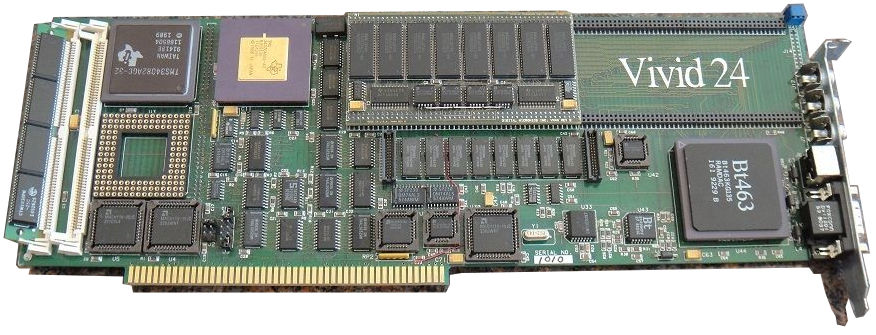
Finally, I’d like to share some heavy stuff: The Digital Micronics Vivid 24.

Yes, it’s an AMIGA Zorro III card, but at heart it’s TIGA… to the max! TMS34020 40MHz, two (2!) 34082 FPUs can be added, max. 8MB RAM and 16MB(!) VRAM… that’s some serious TI-o-rama. In 1992 this beast costs nearly 3000US$   😯

ARM eval boards and Helios

     “Every end implies a beginning.”

This post started out as a special Helios article, but given the rarity and historical importance of the used hardware, it’s now somewhere between the worlds of OS and Hardware – and the combination marks the end of an operating system and the launch of an incredibly successful processor family.

Helios is most likely already one of the loneliest OSes on the planet… I estimate about 10-20 active Helios installations of the Transputer version currently running. But the Helios ARM version supposed to run on my VLSI ARM eval boards is probably the only one on planet Earth.

Quick history digression

Talking about lonely… The  eval boards we’re discussing here, the VY86PID family, was what you could buy from VLSI. VLSI  founded  ARM Ltd. together with Acorn and Apple.
So you’re actually looking at the birthplace of your mobile phones processor right now. This is, where it all started!

When you’ve planned to build a computer based on VLSIs range of ARM CPUs back in the days – most notable the ARM6xx, 7xx and ARM7500 series – you got a VY86PID board . And because not many did – mind the Acorn RiscPC and Apple Newton – those boards are rare as hens teeth today. Googling for it will most likely bring you back here 😉
There’s just one good, original source of information left: The page of Art Sobel himself, Hardware Applications Manager for Embedded products at VLSI Technology, father of the boards discussed here.

Last question: “Why VY86PID? That sounds Intel’ish, like the x86 family.”
Well, VLSIs official name for their ARM IC range always started with VL or VY86… so  for example the fist mass-produced CPU, the ARM2, was officially called VL86C010. It’s memory controller was VL86C110 and they used  VY86C610 for the ARM610.  Only with the introduction of their last ARM CPU, they changed it and called the ARM7500 VY27073B

Hardware

But now, let’s have a look at the eval boards first…

VY86PID 2

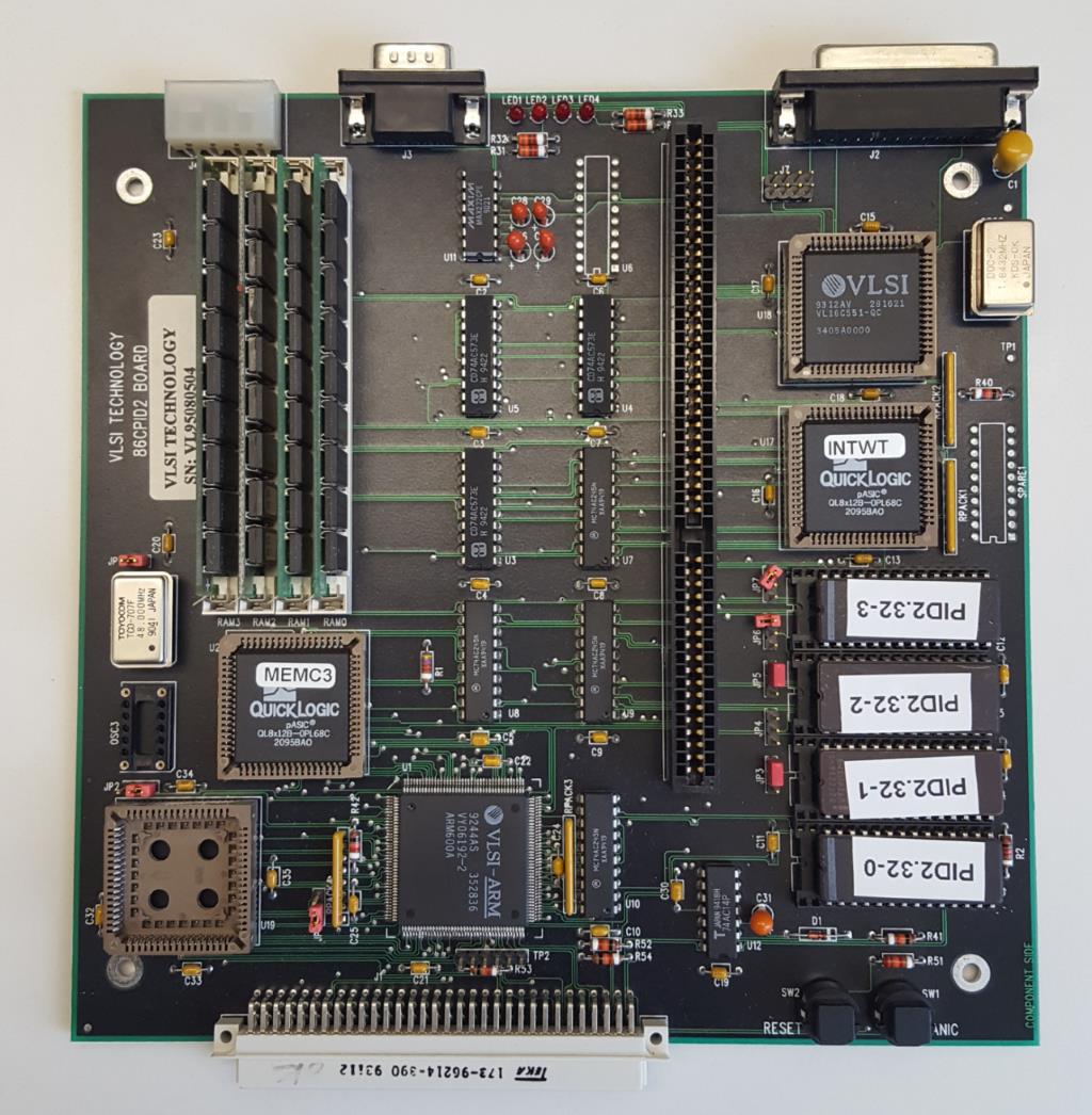
This is the earliest implementation of a PID I ever saw and own. Its components are:

  • ARM600 CPU at 30MHz – soldered onto the board
  • 4 SIMM slots for 1-16MB RAM
  • MEMC3 memory controller on a 12MHz bus
  • ‘INTWT’ INTerrupt (With Timer) controller (Maybe a VL86C410 derivative)
  • VL16C552 Serial/Parallel controller serving an on-board connector each
  • 128KB-1MB ROM (jumpers used for setting the size)
  • one ISA compatible expansion slot
  • 4 status LEDs, Reset- and Panic-buttons
  • an empty PLCC68 socket for the FPA10 FPU from GECPlessey
  • edge-connector to connect a ‘logic analyzer probe board’

It’s worth mentioning that both controllers, the MEMC as well as the INTWT were implemented in QuickLogic ‘pASIC’ QL8X12B 1st generation FPGA. That’s about 1000 gate arrays – tiny in today’s measures. That’s interesting as the MEMC was available as commercial ASIC already – but it that could only support 4MB explaining the appended version number “3”.
Also, take note that the PID2 uses an ARM600, not the later widely used 610 (RiscPC, Newton 1xx series). The 600 features support for a floating point co-processor, ARM Ltd. usually used the term floating point accelerator – this was only supported with the ARM600 & 700 and later integrated in the ARM7500FE.

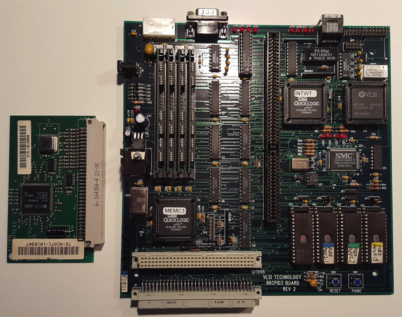
VY86PID3

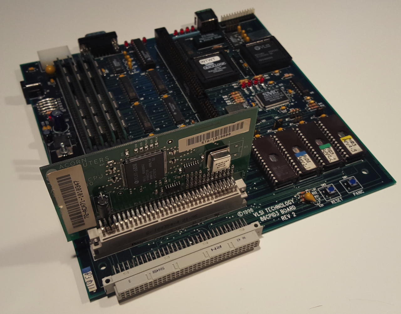
This is the PID3, sometimes also written PID III – this time it’s processor-independent for ARM610, 710, and 810 CPUs, featuring a connector for a CPU module which is 100% compatible to the ones used in the Acorn RiscPC.
Most parts are similar to the previous PID – even the FPGAs – so these are the notable differences:

  • No CPU on-board – instead it offers a slot
  • 10BaseT Ethernet port (SMC 91C94) with 4 status LEDs
  • the empty PLCC socket was removed

Luckily I got an extensive manual with it, even containing all the schematics. Boy, those were the days, when manuals were real manuals!

vy86pid3b

The PID3 with (dis)connected CPU board (it’s an ARM710 card from Acorn RiscPC)

vy86pid3a

So far for the hardware. Both run a rudimentary monitor program from ROM – so let’s have a look into that…

Software

Out of the box the PIDs run a monitor program called “DEMON”, short for DEbug MONitor.
As with most single board computers (eg. Motorola VME boards) those monitors are more or less command-line BIOSes with some debugging features (read/write memory & registers) and are mainly used to load binaries and start them.


The toolchain which came with the eval boards is available here. It even includes a (cross)C-compiler and libs in source!

Helios (so far…)

This was the reason why I bought the boards – getting Helios run on ARM. The original Helios sources which I’m hosting on github also came with a kernel for ARM, specifically the Acorn Archimedes and, well, the PID2…

Historical side note: Why Helios on ARM?

Well,  at the time this port was done it became obvious that the INMOS Transputer wasn’t developing as fast as other CPU families did and so Perihelion, like other INMOS customers,  turned towards alternative architectures.
Also they looked for more profitable market: “The emphasis by this time was to make an embedded real-time system rather than an interactive Unix clone” [Nick Garnett, designer of Helios]
Set-top boxes come to my mind… and later SGS-Thomson was quite successful in that area with their Transputer based ST20 family.

There are 2 supposed ways on getting Helios onto a PID – both using an RS232 connection:

  1. load the kernel through the Helios server (that’s the DOS/Unix terminal tool) which then talks to the DEMON or
  2. Have Helios burned into EPROMs instead of DEMON.

I wasn’t able to get the EPROMs work (binary image here) – or more precisely, connect to the system. It didn’t accept connections from the server, even the readme says so. The LEDs a showing a heartbeat pattern, so I assume the kernel is running – but without a shell connection I can’t tell more.

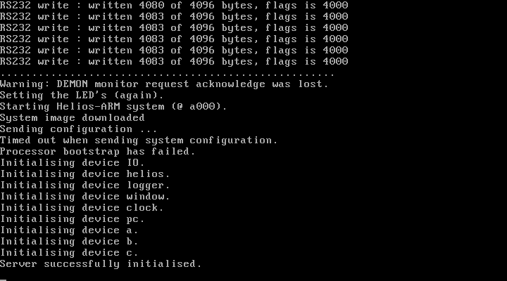
The alternative way by uploading through the server looked more promising… I got it stable at 38400 baud and using the debug flag (ctrl-shift-c) I could see the bytes flying upwards…

…but then it looses the connection, misses an ACK and then  fails to send the system config.  The server – while successfully initialized – then sits and waits forever  😥

To be continued…

2017 updates

Boy, it’s dragging along these days… at least for this page – but rest assure, things happening:

  • Behind the scenes I worked on the 3rd run of AM-B404 TRAMs. If you want one or two, mail me.
  • A small AVM T1 update: Found another revision without any connectors for a booster-board.
  • Got the nice Miro highRISC card out again and did some more digging and reversing…
  • Added another machine to the Systems section: Henkelmann, a portable 486 pimped to the max…
  • Copied the ‘Manufacturing PCBs in China‘ from the Blog into the Knowledge-base section as it got another update… 4 companies reviewed now.
  • After roughly 25 years I got somehow pulled into 68k Mac vortex again – and mysteriously 4 Macs popped up in my lab. While this is not a section on GeekDot (yet), that’s another project currently keeping me busy…


Henkelmann

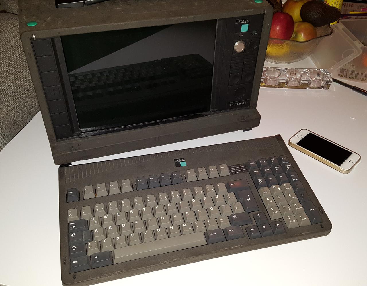
May I introduce you to Henkelmann – a heavily modded Dolch PAC 486 “portable computer”.
‘Henkelmann’ is post-war German miner jargon for a lunch pail – today it is still often used for “anything big with a handle”… and for todays MacBook Air standards the Dolch is quite big. Back in 1998 is was a 32-bit power house…

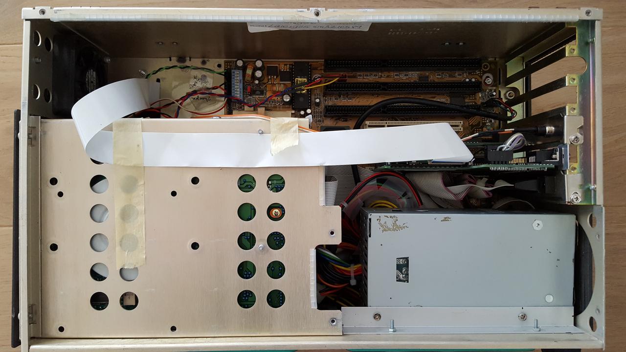
In 2008 I wanted a system with full-size ISA slots (mind Transputer or i860 cards) but a bit speedier than a 25MHz 80486, more flexible and silent (as with some others of my systems) I had to change some bits and pieces. Well, in the end nearly everything was modified. In short:

  • Swapped the tiny 10″ 640×480 for an 12″ 800×600 display
  • …which required a new display controller – PCI only
  • …which required a new motherboard
  • …which made larger IDE drives, CD-ROM and USB possible
  • …which required internal space and connectors
  • all of which required proper cooling or something more power efficient.

Before I go into details, let’s have a quick glimpse: From the front, it still looks pretty original (besides the glossy screen):

The screen

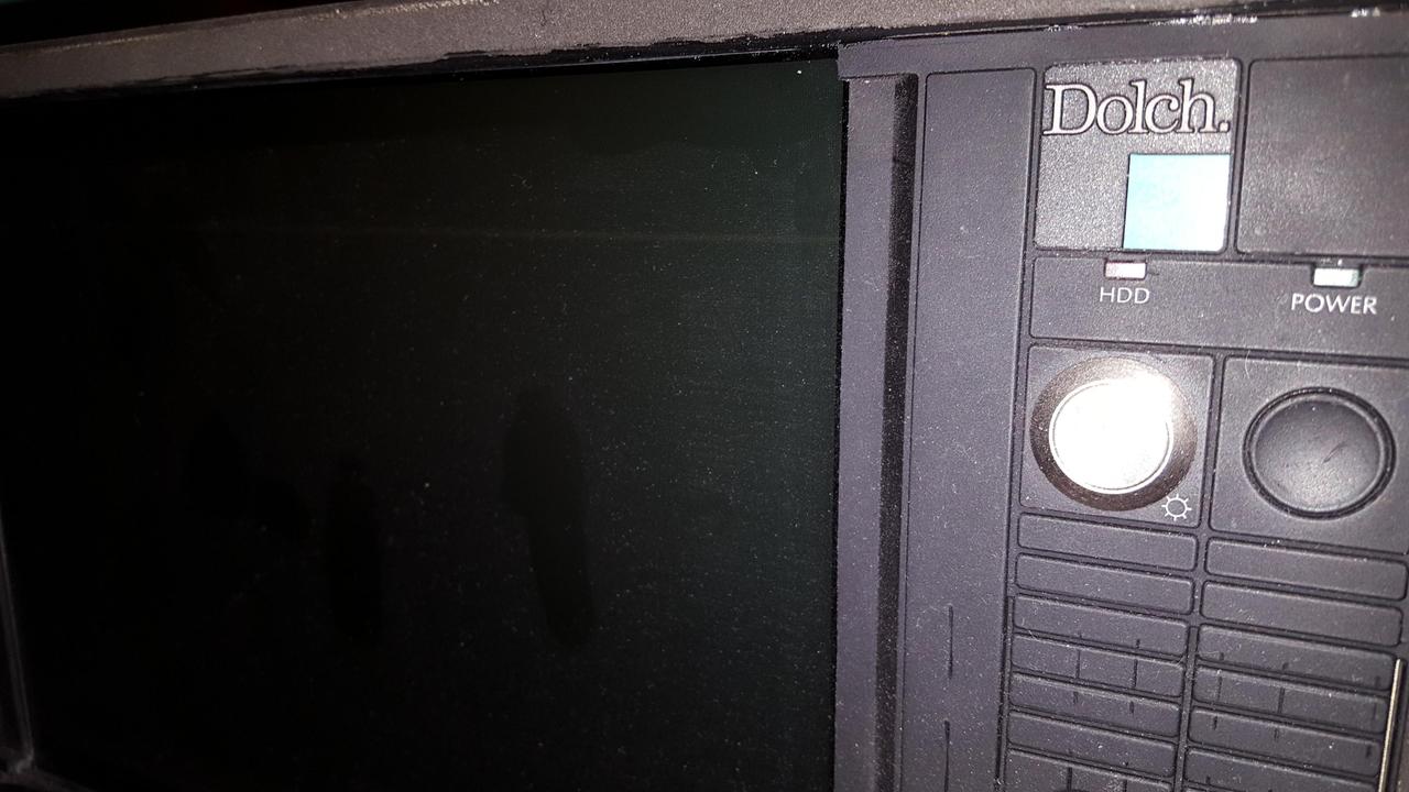
Well, from the moment I’ve opened the ‘box’ by removing the keyboard from the front it became clear that I have to change the small 10″ display which was just OK with its 640×480 resolution to be used with DOS but using Windows was out of question. The original system used an ISA graphics card to control the TFT display – these cards are mostly dedicated to a specific kind of display. So both had to go… and I was able to find a new combo at ePay. Being more modern, the new controller card was a PCI card. But that was totally fine as I was going to change the main-board anyways.

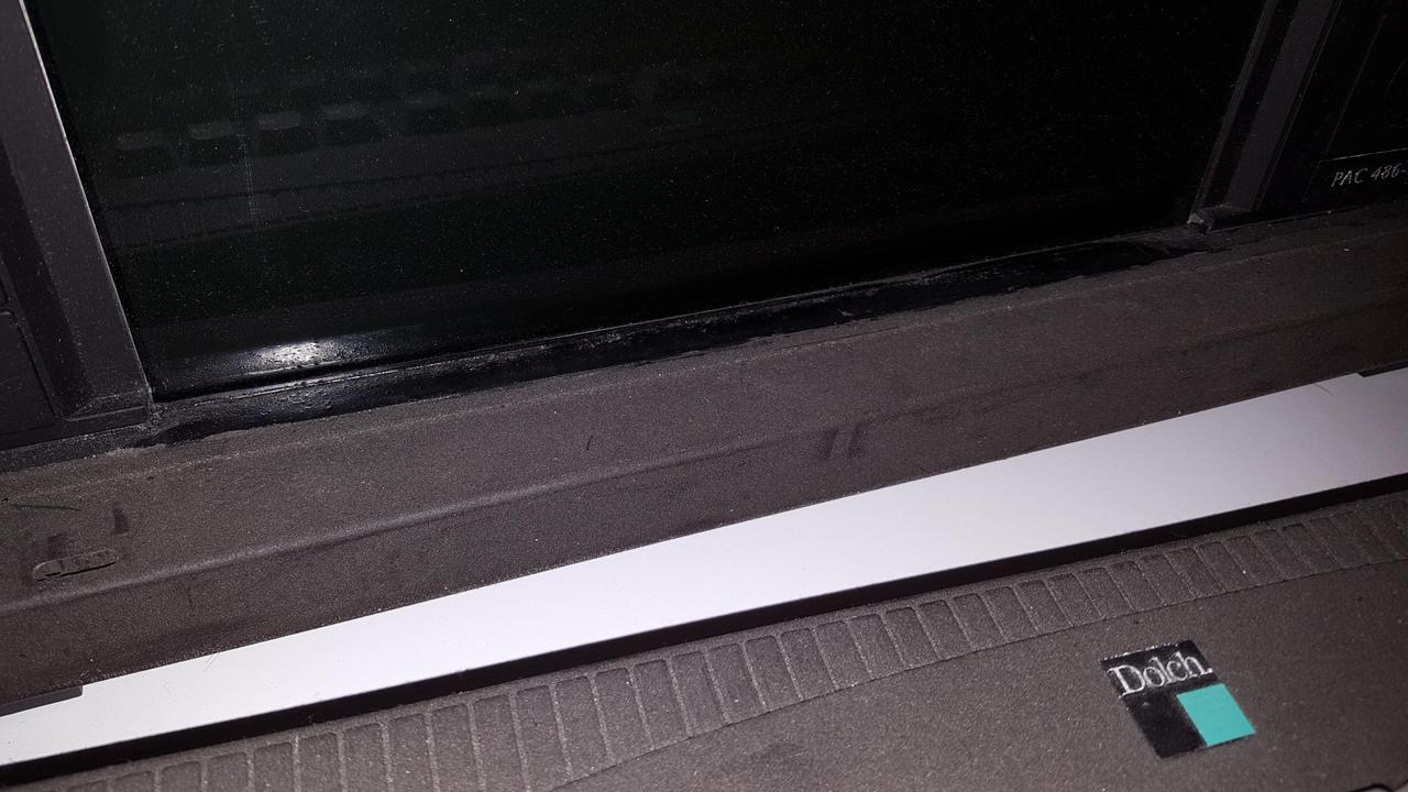
As the new screen was somewhat higher than the old one I had to do some sawing and cutting – so most of the side-panels were removed and luckily the hight perfectly fits between the upper and lower outer-edge, so just about 5mm of the very thick plastic had to be cut out there. The cut edges turned white, so I had to do some (bad) paint job, too. It’s not as bad looking in real than it looks in these pictures:

Bottom edge:

One downside is the fact, that the cables and electronics of the display made it necessary to mount it upside-down – technically that’s no issue as there’s a solder-jumper on the graphics-card to make it flipping the picture. The bad thing is, that the display has an optimized view-angle for just the other way round  🙁 So looking from top at a steep angle the picture looks inverted – from a frontal view there’s no difference, though.

Mainboard

As I wanted the best of both worlds, I needed a baby-AT format for being able to re-use the original case openings (AT-keyboard plug!) but also having as many ‘modern features’ as possible, e.g. PCI, IDE, USB, etc.
Luckily I’ve found the DFI K6BV3+/66 which is a Supersocket-7 board in Baby-AT format… how cool is that?!

Because it’s a Super-Socket 7 board I hunted for the best CPU available for that socket, the AMD K6-III+, a real beast for its time – which I planned to underclock to 266MHz, because I wanted to cool it passively. Well not completely… while the K6-III has a low heatsink on his top, there’s no room left for a fan on top of that.
So there’s a small fan on one side of the case (top left corner in the picture below), sucking air in and blowing it over the heat-sink towards the optional ISA cards… not 100% optimal but worked so far.

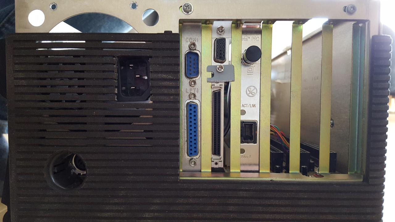
As the K6BV3+ has just an ATC power-connector a new and preferably smaller power supply had to be found. For that, I had to create a custom mounting using an aluminum angle profile (lower right in the picture below).

The power-button went into the NIC back-panel and a new cutout for the power cable was needed:

Peripherals and Drives

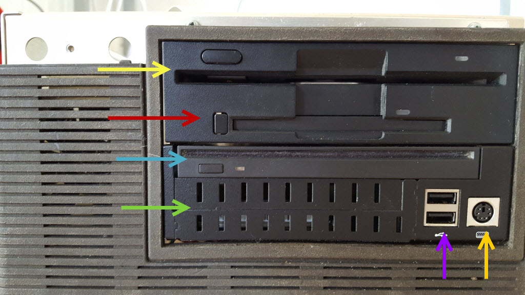
There are just 2 half-height, 5¼” drive slots in the case available. So careful planning was taken to serve every vintage computing need and this is the rather squeezed result:

  • 5¼” & 3½” floppy-drive combo in slot-1 (Yellow & red arrow)
  • Slot-in DVD drive (blue)
  • 2.5″ Harddrive (beneath the DVD, green arrow)
  • 2x USB an 1 PS/2 connector (purple & orange)

Conclusion

All that effort gave me a portable, well, “luggageable” PC which can read and write most media you need for vintage computing. It’s rather fast, nearly silent and most importantly features 2 full-size ISA slots and a shared PCI-slot for more recent stuff.

Digging deeper into the highRISC

After 7 years mainly doing research on Transputers and the i860, I had the feeling it’s time to do some more digging into the highRISC card.
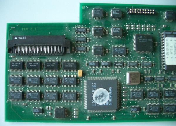
If you have read my initial post about the miroHIGHRISC (and the Tiger) you remember the undocumented 20pin socket on the card (pictured in the upper right corner):

HighRiscLeft

Let’s have another look at the “UART port” again:

The pinout (the connector is rotated 90° counter clock-wise):

GND  oo  /WR0
D0   oo  INT2
D1   oo  /RD
D2   oo  /IOSEL
D3   oo  RESET (most likely)
D4   oo  A2
D5   oo  A3
D6   oo  A4
D7   oo  A5
VCC  oo  A23

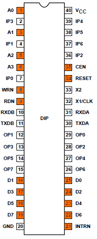
Reading a bit of the BIOS’ disassembly, I stumbled across routines to talk to an UART.  A very common (D)UART of those days was the SCN2681. If you take a look at this chips specs, they perfectly fit to the signals provided at the HIGRISCs UART-port!

Here’s its pinout with the corresponding pins marked:


A2-A5 are used for A0-A3 on the 2681 and the only pin not directly represented is A23 which might be used to decode. Also, it nicely reveals that CPU INT2 is used for the UART.

The LR33000 datasheet tells me that there’s an 4MB IO-area starting at 0x1E000000 reaching up to 0x1EFFFFFF- most likely the 2681 will live there… and the corresponding signal called /IOSEL is available on the UART-port (and will perfectly help as chip-select decoder). Tadaa!

So after the UART we need to get the RX/TX signals to a higher level, i.e. the +/-15V of RS232 – this is the call for our old friend MAX232.

[current bread-board experiments sadly didn’t yield into ‘instant success(tm)’… I’m missing out something – need more time to investigate]

Bootcode / BIOS

The LR330xx CPU also has an /EPSEL EPROM select signal, indicating it’s accessing an EPROM expected to start at 0x1F000000 and ends at 0x1FFFFFFF (4MB right below the IO-area).
Using this knowledge and knowing that the MIPS standard boot-vector is at 0x1FC00000, it’s easy to feed the ROM-dump I did some years ago into the disassembler with the correct start address to do his job.

We need to get an understanding of this bootcode first, so that we can get an idea of “what is where” (e.g. ISA bus, UART etc) and later upload our own code and use those addresses.
Just to stick my head a bit into the clouds, the aim is to first port a then common MIPS monitor-program called ‘PMON’ and use that to run some sort of μLinux. But that’s probably another handful of years ahead…
PMON was a good source of information, because it’s originally written by LSI, supporting all the LSI eval-boards. Lo and behold, some of them had a 2681 UART, too… located at 0xBE000000, which is extensively used in my BIOS disassembly  😉
I have a certain feeling that miro borrowed some design ideas from the LSI Pocket Rocket evaluation board (don’t Google it, it’s a mythic being – if you have documentation, mail me!).

So this is the 2681 memory-map then:

#define BASE_2681 0xbe000000
#define SRA_2681 ((1*4)+BASE_2681) // 0xbe000004 status register 
#define THRA_2681 ((3*4)+BASE_2681) // 0xbe00000C Rx/Tx holding register 
#define ACR_2681 ((4*4)+BASE_2681) // 0xbe000010 Aux contrl. register 
#define ISR_2681 ((5*4)+BASE_2681) // 0xbe000014 interrupt state register 
#define CTU_2681 ((6*4)+BASE_2681) // 0xbe000018 Counter timer upper 
#define CTL_2681 ((7*4)+BASE_2681) // 0xbe00001C counter timer lower 
#define START_2681 ((14*4)+BASE_2681) // 0xbe000038 start timer 
#define STOP_2681 ((15*4)+BASE_2681) // 0xbe00003C stoptimer

Using those addresses we should easily identify the comms routines.

Something happens at 0xBE800000 which seems not UART related. So that’s probably the reason why A23 is available on the connector. That way we can ignore access to that address by OR’ing it with /IOSEL to create a /CS.

The DOS side of things

The tool to load a MIPS executable into the HIGHRISC is called DL.EXE. Loading the test-program prints this to the console:

miroHIGHRISC download program. V 1.00
(c) miro Computer Products AG , Germany

CONFIG: I/O-register-address: 0x368 
CONFIG: DRAM - base-address : 0xD000 
CONFIG: DRAM - size : 8 MB
CONFIG: TIGER - RAM - size : 8 MB

Resetcount = 87340

Loading test.zor
text : start=0x80030000 size=0x52c0
data : start=0x800352c0 size=0x520
bss : start=0x800357e0 size=0x150
entry : 0x800301a0
TIGER comm.address : 0x3ffd00
max_used_address : 0x35930 
real_DRAM : 0x800000 
Heapsize : 0x7CA6D0

test.zor sucessfully downloaded.

This gives us valuable information. The DOS-side uses the IO port 0x368 and has a memory window of 16K from  0xD000 to D3FF.
MIPS programs are loaded to 0x80030000 and the 16K seems to be mapped to 0x003FFD00, just 128K below the 4MB boundary of the LR33k address space.

As usual – this is heavily work-in-progress. So this post will be edited while making any new progress. TBC…

Geekdot got a forum!

This is a short notice that GeekDot just got its very own forum… woohoo! (It’s in the top menu, in case you’re asking)

That’s mainly due to (slowly) growing number of T2A2 users, who should have a place to discuss their projects… that said, all other topics touched at GeekDot are welcome, too.

So register here and start posting! Hope to see/read you soon!

TIGA – The basic stuff

Welcome to the TIGA basics page! The fist post in my little TIGA chapter.
You probably came here because you just got (or plan to buy) a cool, shiny TIGA card and like put it to some use. Or you’ve read about it and found out, that the Web is pretty thin on that matter… Anyway, you came to the right place!

Let’s check some points fist…

Hardware

Well, if you have a card already, great, you’re set.

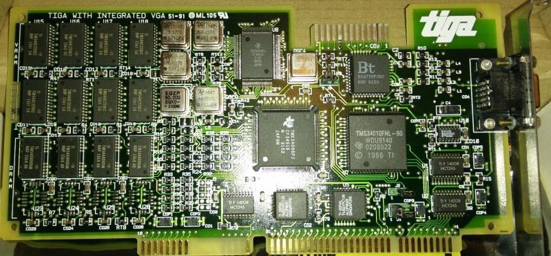
There were/are different versions around. The early cards used the first implementation of the graphics controller called TMS34010  which was clocked up to 60MHz (amazingly high!). For example TIs very own “TIGA Star”:

Later models used the advanced TMS34020 which started at 33MHz up to a max of 40 but had faster instruction cycle times, a faster memory interface and a twice as big instruction cache (512 bytes. Yes, bytes). Additionally the ‘020 supports the rare TM34082 floating point co-processor (actually even more than one) to speed up 3D calculation. I’m not aware of a Tool using that…

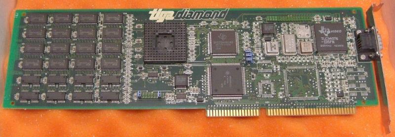
One of the first ‘020 cards was probably the Diamond from TI, which even features a socket for the FPU:

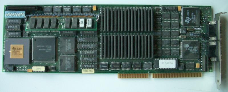
My weapon of choice is the mighty Miro TIGER:

Every TMS340 has its own RAM to run “programs” in. Depending on the model this starts at 1MB and can sometimes expanded up to 17MB. Better cards used SIMM to do this, but there were some models which used  proprietary RAM modules which are nearly impossible to come by these days.
Next the TMS340 needs VRAM, the memory holding the graphics itself. Again, depending on the model, this might vary from 1 to 4MB resulting in different max resolutions. IMHO just 1MB doesn’t do a TIGA card justice. That is just enough for 640×480 in 24bit…
Finally, as TIGA was not a standard CGA/EGA/VGA replacement, you’ll need some way of displaying the DOS text/graphics output. TIGA was always meant as an additional display mostly using a 2nd high-resolution screen, so TIGA cards either run in parallel to an existing VGA card or it also features a (mostly simple) VGA controller for this.
Very sophisticated cards like the above miroTIGER gave many options for this. It features a small VGA part (a Cirrus Logic CL-GD540 and 256K of DRAM) to make a 2nd card unnecessary or could disable that to use a 2nd card of your choice for a two-screen-solution or offered to loop-though the signal of an existing VGA card and automatically switch between them for a single-screen-setup.

Recommendation

So if you consider buying a TIGA card, go for a TMS34020 with SIMM sockets. It should have at least 1MB RAM and 2MB of VRAM. A SPEA Graphiti FGA is a good example for this minimum config.
While DRAM isn’t that important, the more VRAM you have, the better. Having a VGA controller on board might be desirable if you’re tight on slots – but to my knowledge the best VGA controller ever used on-board  was an ET4000. So it’s more or less a matter of taste.

Software

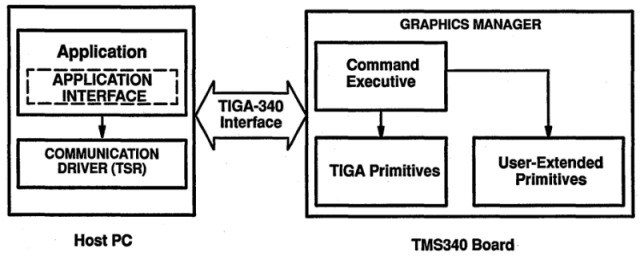
Actually this is the more important point on your list. While yes, TIGA is a standard, it contains certain proprietary parts, called the CD, GM and EXTPRIMS you’ll need to get your card going. The reason for this is the driver which is more a layer model looking like this (listed bottom-up):

Application using TIGA (e.g. AutoCAD)
application specific extensions (also *.ALM/*.RLM file)
extended primitives (EXTPRIMS.RLM/*.ALM)
Graphics Manager (e.g. tigagm.out)
Communication Driver (tigacd.exe)


The 3 yellow(ish) levels are card-dependent, so without them, you’re lost and your shiny TIGA card just makes a nice paperweight.
The lowest level is the Communications Driver, or CD for short, is 100% hardware dependent –  It is always supplied by the cards manufacturer and, well, handles the low-level communication and resides in the PC (upper-)memory.
Above that sits the Graphics Manager (GM)- this is the “real thing™”, the core or kernel of TIGA – which is the firsts thing being loaded into the cards own DRAM.
On top of the Graphics Manager sits another layer belonging to the package provided by the card manufacturer and loaded into the cards RAM, the Extended Primitives Library called EXTPRIMS.RLM in 99% of all cases. This contains all the drawing routines for primitives e.g. boxes, circles but also printing text etc. The file extension ‘RLM’ stands for relocatable load modules while ALM means absolute load modules. RLM’s are loaded and linked at run time, ALM’s are linked in advance for a fixed configuration and later at run time just loaded onto the TIGA card.

Here’s another illustration to show the layer model separated by memory regions:

With these 3 layers loaded, your TIGA card is ready to rock and awaiting commands from your application. Let’s take AutoCAD as an example – it’s probably the best example anyway as TIGA was mainly used for CAD.
It will not only load the TIGA driver but probably also some extensions provided by your cards manufacturer. So for example the miroTIGER came with a 3D-Viewer called “MulitVIEW”, ELSA provided a tool called ELSAVIEW with their Gemini cards etc.. All those tools loaded some extra code into the cards RAM (that’s the light blue layer).
All the extension tools I saw up to now didn’t require more than 200KB RAM. The TIGA core itself is at ~100KB, so for most basic stuff 1MB might suffice at first – but of course some of those tools need extra RAM for holding data so my assumption is that 2MB are a good bet to start with.

Caveats

All that said, be aware that were two main versions of the TIGA kernel – V1.x and V2.x which have slight differences in programming. Again, it depends on the model of your card which TIGA version is supported. As far as I know, V2.x (2.2 being the latest) requires a TMS34020.
ALM’s were a unique feature of TIGA V1.1 and should no longer be used with TIGA V2.0. Generally, V1.x programs do not run (properly) on a V2.x CD/GM combo.

Setup

First, most likely there might be something to setup on your card. DIP switches for example or jumpers. At least you need to know/set the base-IO address of your card. Lucky are those who have a manual 😉
Next, as this is DOS-land, there are some things to set-up in your config files. As usual with DOS, you have to set an environment variable in your AUTOEXEC.BAT:

SET TIGA=-mC:\TIGA -lC:\TIGA -i0x60
PATH=%PATH%;C:\TIGA

This defines the path(es) to your TIGA modules and libraries as well as the base-IO address, at which your card is communicating. This has to be adjusted to your hardware setting.
Also the base-path to your TIGA files needs to be in the system path.

Then you load your CD and (optionally) GM:

lh C:\TIGA\TIGACD.EXE
lhC:\TIGA\TIGALNK.EXE -LX

The 1st line is clear – if your config allows, you can load the CD into upper-memory. With the 2nd line you can pre-load the GM into the cards RAM and the -LX parameter makes sure it eXecutes right after that. This step is optional, as well programmed TIGA programs check for the GM and if it’s not loaded, they’ll take care of that.

That’s about it. Yay, your TIGA system is up and running 😀 and you’re ready for some action.

The next post shows how to program your TIGA card and do some graphics…

SPARC – time flies

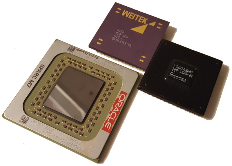
Recently a good friend of mine gave me a super-duper, crazy-as-hell Oracle SPARC M7 CPU for my CPU collection forcing me into another stroll down the memory lane… and I couldn’t refrain from taking a special “family photo”

SPARC M7 next to SPARC 1 - 29 years appart

Yes, the couple sitting next to the huge M7 is a SPARC (1) from a SPARCstation 1 @ 20MHz, – the CPU was manufactured 1989 by LSI (S1A0007), the FPU came from Weitek (3170).
BTW: I personally pulled both back in 1992, when I worked in my 2nd company selling SPARC clones.

If I counted correctly, the there are 26 model-generations and about 29 years are between them (just SUN/Oracle models). Ignoring all the M7 hyper-modern stuff like in-silicon-SQL accelerators etc. numbers are still breathtaking:
The SPARC M7 -still one of the fastest CPUs around (as of 2016)- has  10.000 times more transistors, a 206 times higher clocking, 31 more “cores”. It’s 64MB L3 cache(!) is the same amount, a SPARCstation could address as a maximum system RAM.
Sadly there’s no way to compare their actual computing power, as benchmarks which where ran on the SPARC 1 aren’t applicable on the M7 and vice versa. Or do you have Dhry/Whetstones for an M7?

Anyhow: It’s just so amazing to be able to witness this crazy development in just 2/3rds of an average-life-time. Don’t you think so, too?