
Again, Geekdot.com might be the only place left in the World Wide Web where you can get more information about the flopped mysterious T9000 than what you will find on Wikipedia.
The T9000 never made it into the market in higher volumes. I don’t have any numbers on how many T9000 were actually produced but only a few were evaluated outside INMOS by universities and science facilities, most famous is probably the CERN, which did some benchmarks and tests. Here’s a (now funny) promotion video of those days:
By another lucky incident I got myself a HTRAM mainboard for Christmas 2011. It’s the QT9M from Quintek, a spin-off of INMOS back then. Three slots of this 6-slot board were populated, one featuring the mythical T9000!
This is the naked board, the QT9M:
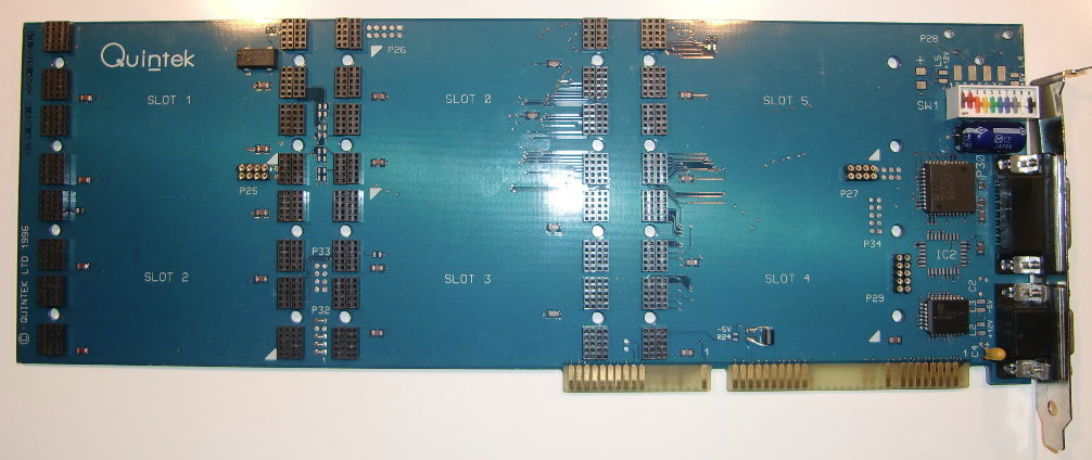
At the first look you can see it’s a damn huge thing. At least one inch taller than the slot-backplate. But this way Quintek could squeeze 6 size-1 HTRAM slots (3×2 slots, horizontally) onto the card, while the “official” INMOS B108 (PDF) board just features 2 slots (but size-4, vertically).
The HTRAM slots in detail
(-> For a complete description of HTRAM visit this chapter of geekdot.com)
Not all slots are offering the same features, though. Slot-0, slot 3 (the two middle ones) and slot-2 (lower left) offer the standard pin-blocks 1 and 2 as well as block 3 and 4.
slot-1 (top-left) offers the same pin-blocks but also a small 4×2 horizontally aligned block on its lower edge.
The same 4×2 pin-block can be found on HTRAM-slot 5 (upper right), but this time only the standard pin-blocks 3 and 4 are featured.
Finally, on slot-4 (lower right) only the standard pin-blocks 3 and 4 are featured, too, but it also has a 5×2 pin-block centred to the opposing edge of the standard pin-blocks.
My assumption is that pin-blocks 3 & 4 offer a direct connection into the T9000 memory map, so I’d call slot-4 & 5 “mem-mapped-ony slots”.
The interface logic
The interface logic on the board was kept surprisingly simple. Especially when you compare it to the already mentioned IMS B108, which had an FPGA and two C101 protocol converters.
Without any C101 you can be assure that there won’t be any downward compatible communication as we are used to with the T4xx/T8xx Transputers (OS-Link), so this will be a hard nut to crack :-/
Let’s have a closer look at the “logic side of things”:
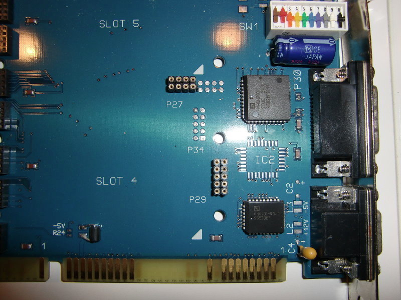
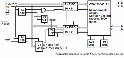
There are only 2 ICs: An AMD MACH 210 CPLD and an AMD 4701, which is an 8-bit bi-directional 512 byte deep FiFo Buffer and parity-generator. Given the fact that there’s a place left for IC2, I assume a 2nd 4701 could go there to make the interface 16bit wide (as all 16 ISA data-lines are connected on the slot-connector).
This leads to my totally uneducated guesses, that:
- The DS data-links are directly connected (through the FiFo) to the ISA bus
- The control registers of the AM7401 needs to be set – if the default state is not sufficient
Quite a solid foundation to those assumptions is the following schematic I was able to dig out of the depth of the internet describing an IEEE 1355 interface. IEEE 1355 is the standard which was created out of INMOS’ DS-Links.
Everything else…
The function of the colourful DIP-Switch is yet completely unknown. It’s clear that some of these switches will set the base-address for communication with the ISA bus.
The sense behind the two Sub-D connectors at the cards backplate are unknown, too. Maybe some link-outs?
(To be continued…)