Tag Archives: graphics

ATW800/2

Current Mega-ST version

Welcome to the ATW800/2 page – read that as you like:  “ATW800 two” or “ATW800 half”, depending on your expectation.😉
Whatever way, it’s the Atari Transputer Card as it was meant to be.

This is a pre-announcement – July 2024

Normally I do not talk about things which are still in the works.
This is an exception to the rule to inform “the scene” and especially other creators of hardware to prevent unnecessary diversification and fragmentation of an already small market.

I personally hate to buy a piece of hardware just to learn some time later, there’s another one available I wasn’t able to compare to the one I just bought.
So this is a ‘shoulder look’ for you to get an idea what’s coming.

To be dead sure: It already works. It will be released. It’s just not 100% done yet.

And for those, who haven’t watched it… here’s the hastly made YT video 😅

Background

Before we go into features & technical details (skip to those if you’re impatient) I’d like to talk a bit about motivation and goals of this project.

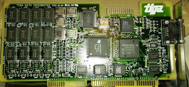
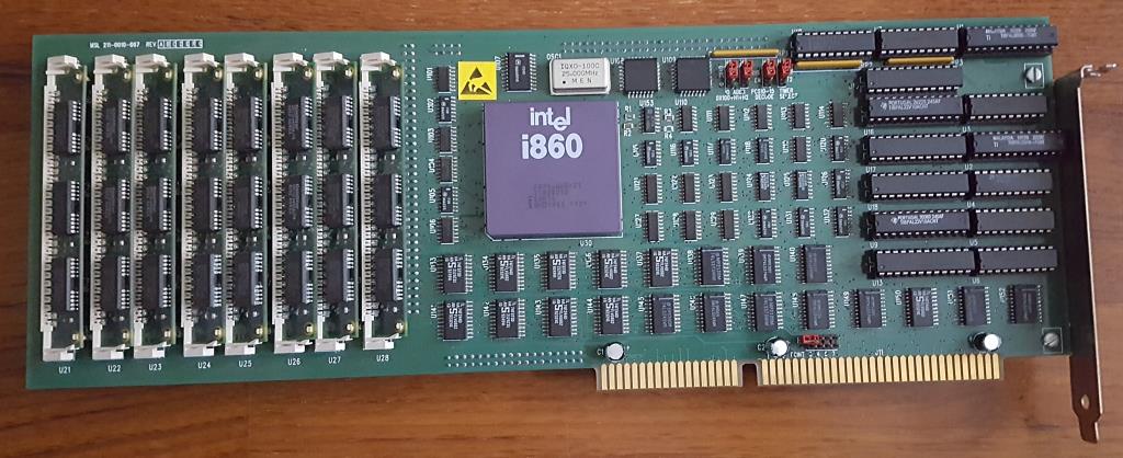
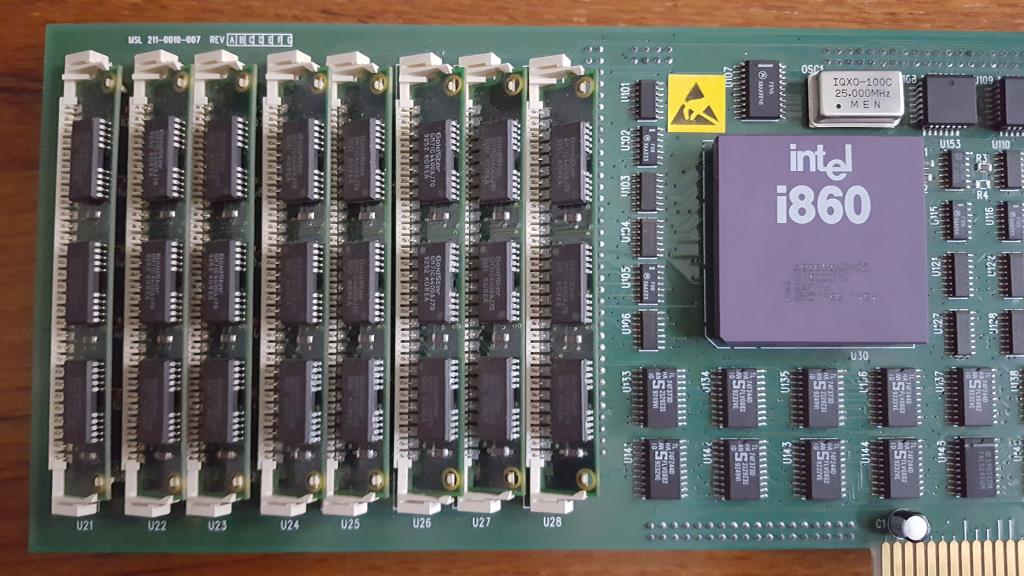
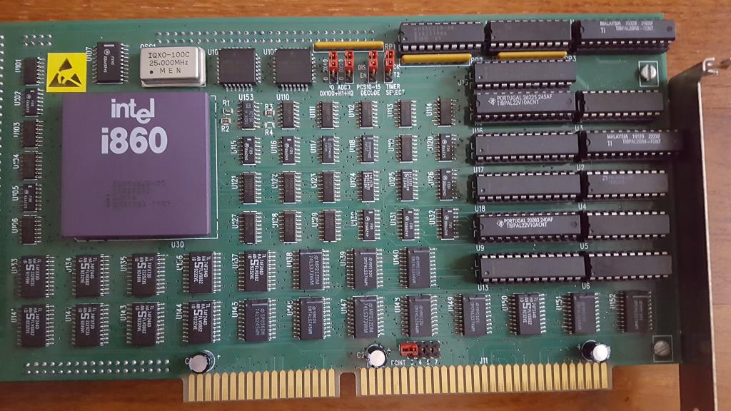
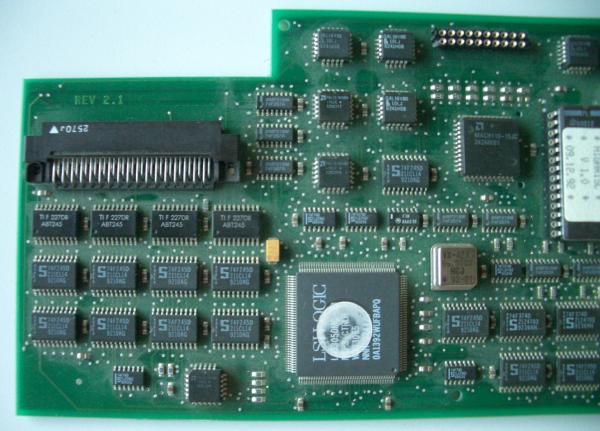
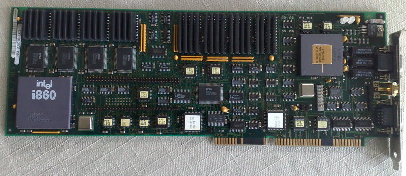
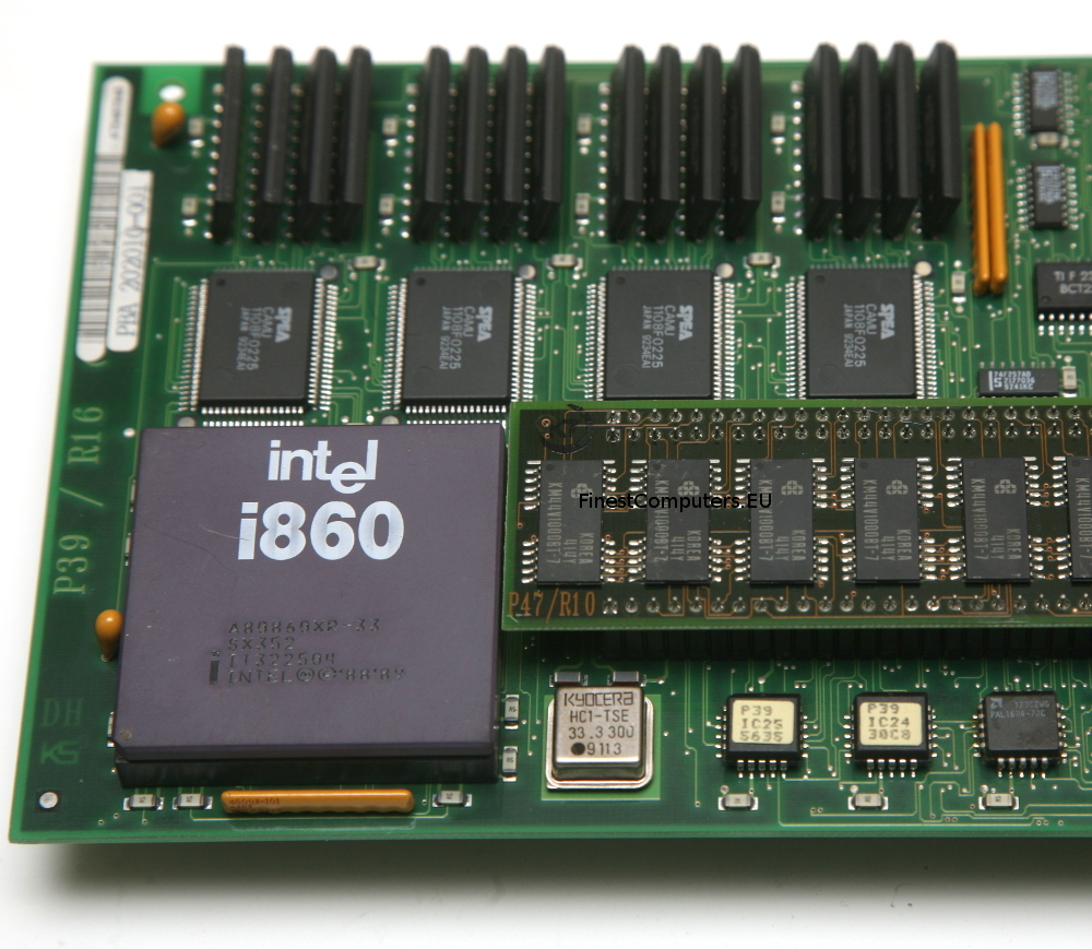
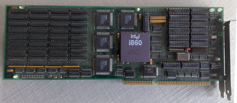
You might have read about my STG[A]TW card for the ATARI Mega-ST expansion bus. That contained an ET4000 graphics card borrowed from IBM PC ISA-land and an Inmos C011 Link-Adapter to connect to a Transputer CPU.
This showed the direction but was a bit cumbersome. Also, ET4000 cards are getting hard to find, expensive (>100€) and not all of them actually do work in your ATARI – and most important, my intention was to create something affordable – remember: Power without the price ✊

The idea is/was to provide a plug-and-play version of a expansion which brings your ATARI as close as possible to what the ATARI Transputer Workstation (ATW800) provided.
That is: Transputers of course as well as expanded graphics capabilities.

Here are my 5 goals I want(ed) to achieve:

  1. Be reasonably ‘historically correct’
  2. Create a design avoiding obsolete parts where possible
  3. Stay in a affordable price range
  4. Simple installation
  5. Integrate/play nice with other peripherals
  6. Offer options

Goal #1 is a philosophical topic one can discuss for his/her whole retro-nerd life. It’s the same as with e.g. cars. Is it OK to put a US V8 into a Ferrari? Electrifying a 1970 Porsche 911? LED headlights in a vintage car? Trailer Queen or patina? The list and discussion will go to the end of humankind.
The very same goes for vintage computer systems. There’s nearly none left which hasn’t had a Raspberry Pi of some sort slapped into it. Starting with a Pi Nano as WiFi-module and ending with a full blown 1.5GHz Pi 4 in an 8bit machine… for my taste, this is not the way.
So with this project we stay with what would have been possible in the let’s say 90s. It might be reached by using more integrated parts, but no recent high-tech here. Sorry. Which brings us to the next point…

Goal #2 is more or less a financial decision. If you use parts which are long time out of production, you depend on a grey market which is limited and can quickly drain, might be full of fakes and prices explode due to greediness.
So instead of buying the last stock of e.g. ET4000W32 chips and create a redesign of an x86 ISA card kludged onto a 68k bus, it’s wiser to go for a ‘virtual design’ which won’t go EOL and can grow as we go… in this case: FPGA is the wayBut following goal #1, don’t overdo.
If there’s (currently) no other option, we obviously have to go with the old parts. The Inmos C011 link-adapter is an example here.

Goal #3 limits #2 in some aspects. It’s relatively simple to pick a recent FPGA which actually would be capable to easily simulate your whole ATARI ST (or two)… but that would be quite expensive – not just the chip but also the design, which requires external RAM, 3-4 voltages and multi-layer PCBs to cope with 200+ BGA connects.
The compromise here is an FPGA board which offers all that already mounted onto it and will be piggy-backed onto our card.
And because cheap is always a challenge, we went for the Chinese Nano FPGA family which has an unreached price/feature ratio and fits the “Power without the price” mantra.

Goal #4 is quite simple: Not everybody is a virtuoso with his/her solder iron. So I tried to avoid as much additional soldering/cabling as possible.
Basically you plug the card into the Mega-ST or VME slot and you’re good to go.
In fact, as of today, there’s just one cable to plug(!) if you want to use one optional feature of the ATW800/2 (ACSI INT). No soldering whatsoever.
Also, you should be able to plug the card in and use it without additional needs. That’s why it offers (optional) TOS ROMs.
This is the way 😉

Goal #5 reflects the awareness that there are mostly souped-up machines out there. I daresay no one who plays with uses his Atari unenhanced in one or the other way.
The ATW800/2 tries to play nice with other common expansions by precisely decoding (previously unused) addresses and even integrate their features like the looped-through USB port of the Lightning-ST.
That said, there are so many old and new peripherals that nobody can guarantee that everything works nicely together with an ATW800/2 – especially on an overloaded bus.

And because of this Goal #6 will be covered by “bespoke ordering“.
Not everybody will be interested in having 2 TRAM slots for hosting real Transputers – so you can leave them out and save some €€.
The same goes for the TOS ROMs. If you already have another ROM switcher, just leave it unpopulated.

Reality kicked in

Having all that planned out, back to the drawing board I went… just to realize that I cannot handle that all by my self.
So it became clear that I have to ask specialists if they like to join the effort.
Let me introduce you to the team aka “The league of extraordinary Transputer gentlemen“:

  • Wolfgang ‘Idek’ Hiestand of the Nova drivers fame.
    Back around the start of the 2000s, Wolfgang looked into getting his hands on the Nova source code with the intention of preserving knowledge about Nova cards. It took some time, but in the end he succeeded in recreating the original drivers. Since then, he has maintained and extended Nova drivers to support additional VGA cards and ATARI computers. For this project, Wolfgang has created a branch of the Nova drivers to support the FPGA-based card.
  • Claus Meder. God of all things FPGA and fellow Transputer maniac. So much actually that he wrote a Transputer core in VHDL.
    Claus designed and wrote the impressive graphics-core for an FPGA from hell.
  • André Saischowa. Atari and Transputer fiddler of the earliest hours. He wrote Transputer and Atari ST programs back then and just got into the matters again when we met. Perfect timing!
    André ported all INMOS tools as well as the Helios server… plus developing  driver .sys files for NVDI.
  • Honorable mention: Mike Brüstle of transputer.net. The man whose brain natively runs Transputer assembly code.
    When you have a question regarding Transputers and he doesn’t know the answer, nobody does.

All four of them have many, many more talents and without them this project would still be just another dream of mine. ❤

Features

Ah, finally… features.
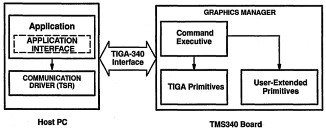
I assume you’re roughly in the picture, what the ATARI Transputer Workstation was all about. Basically, it was a Transputer system running Helios  which used an Mega-ST1 as host. The powerful graphics chip (“Blossom“) was connected to the Transputer which ran X11 on it to display graphics in 1280 by 960 pixels (16 colors) or 1024 by 786 pixels in 256 colors, making the most out of its 1MB VRAM.
As said the Atari part was mainly just I/O: Harddisk, keyboard, mouse, serial and parallel interface. No access to Blossom and after booting, there was no way to run Atari software from/in Helios.

Today that’s bugging me, and like said before, I think Atari or Perihelion, the company behind Helios as well as the ATW, took the wrong approach.
The Transputer system should not sit on top of the Atari system but next to it. Both, TOS/GEM as well as the Transputer(s) should have access to all that pixel beauty.

So there you have it, the two main features and ‘raison d’Être’:

High-Res color graphics 👾

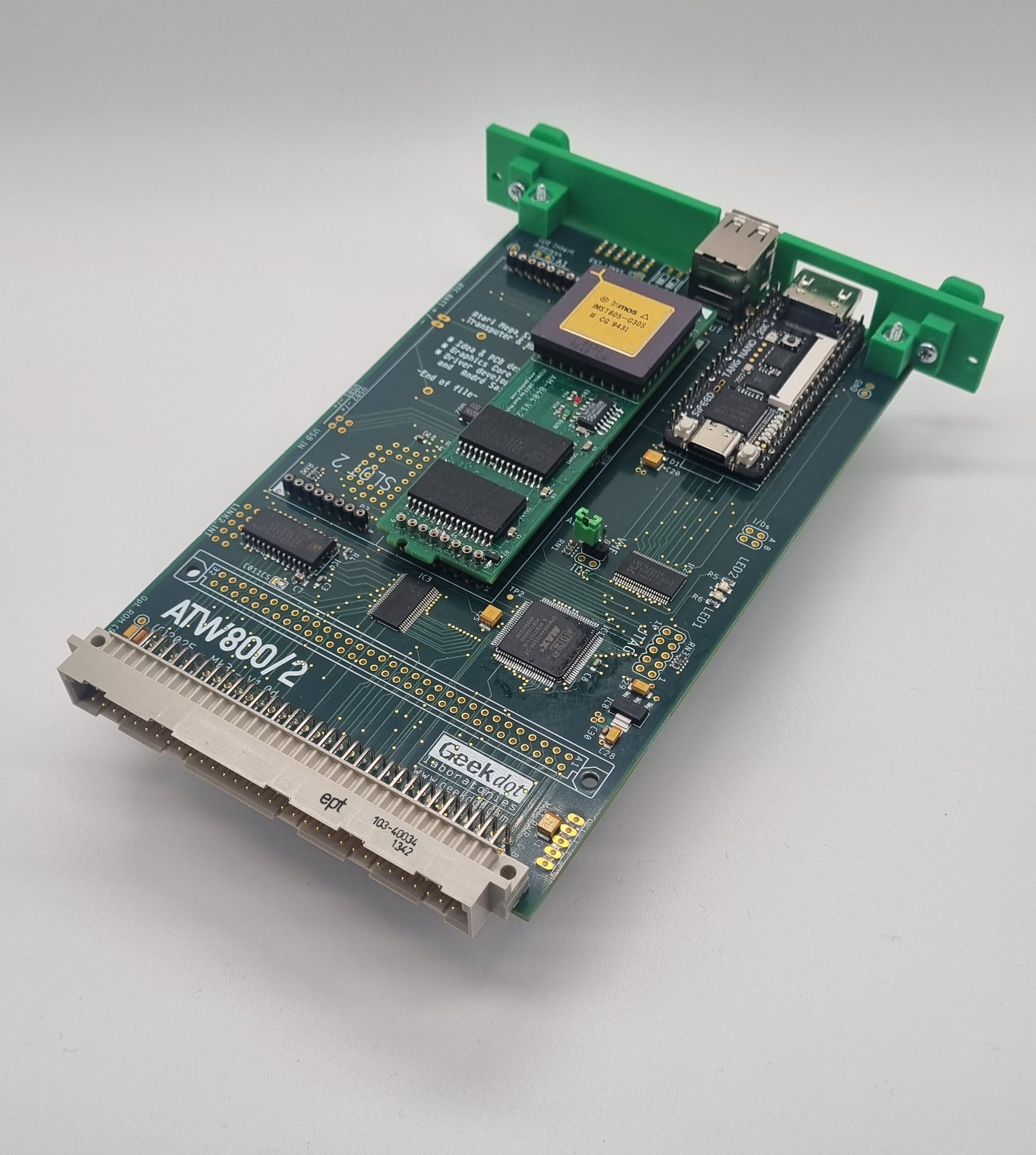
The ATW800/2 graphics controller is actually a tiny and cheap FPGA board piggybacked onto the card. While we started out with the Tang Nano9k it soon proved to be unstable as soon you stretched it to the max… as for now, we changed to the slightly more expensive Nano20k which therefore offers more room and faster/bigger RAM.
[NB: This is the prefect proof that it does make sense to keep this part “virtual” – no shortcoming or chip EOL’ing can stop the product itself. All it needs is an adaptor.]

Displays will be directly connected to its HDMI port. If you need VGA output you could use an HDMI to VGA converter available at ~8€ (See FAQ for that).

The running core, called “Seurat” (named after the inventor of Pointillism), has access to 2MB of VRAM, which is twice what Blossom had. Thus there are quite some resolutions possible (in 2,  8 and 16 bit colors):

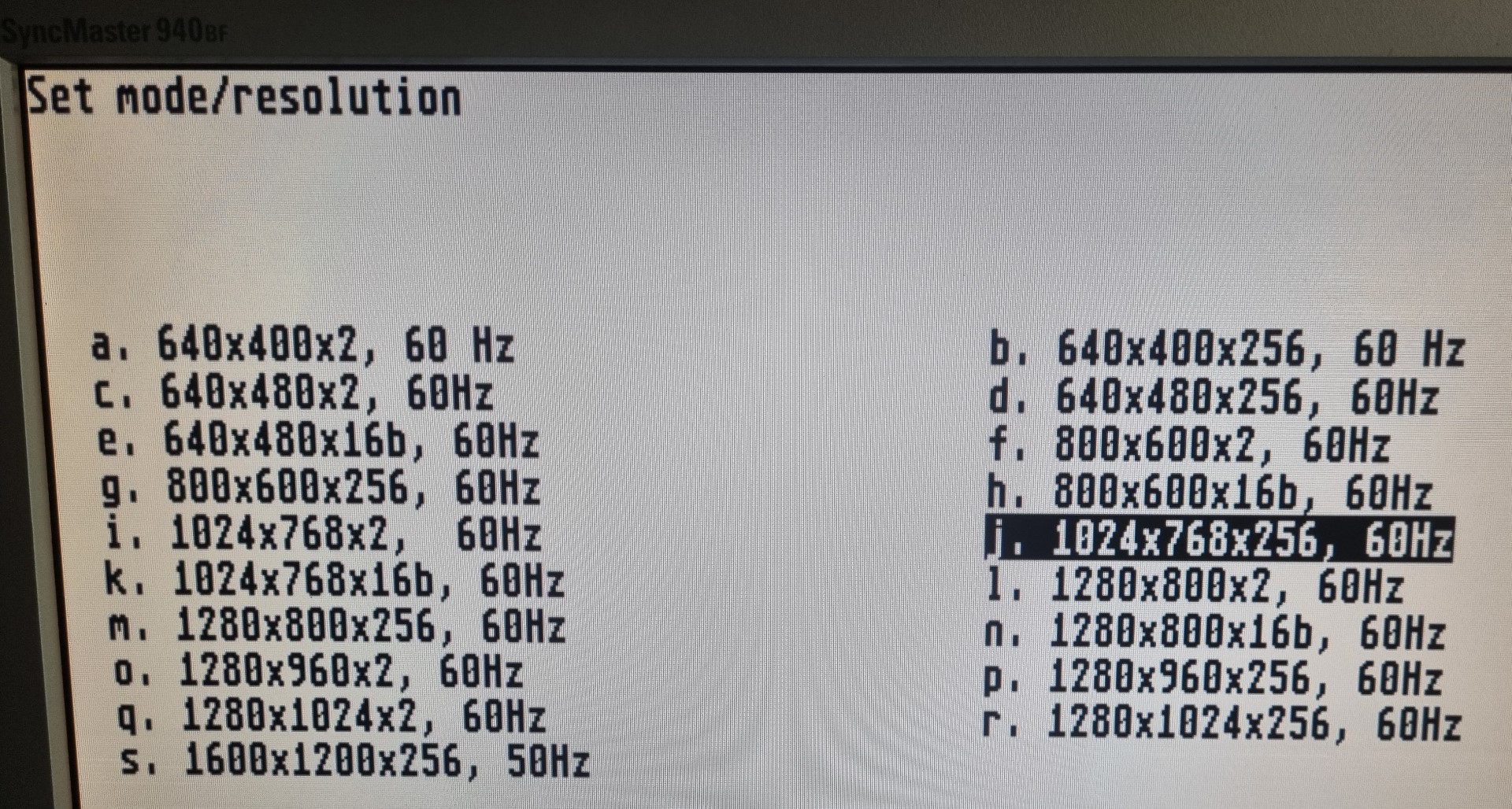
Woo-hoo… holy Bat-Resolution! 🤯 (1600×1200@256)

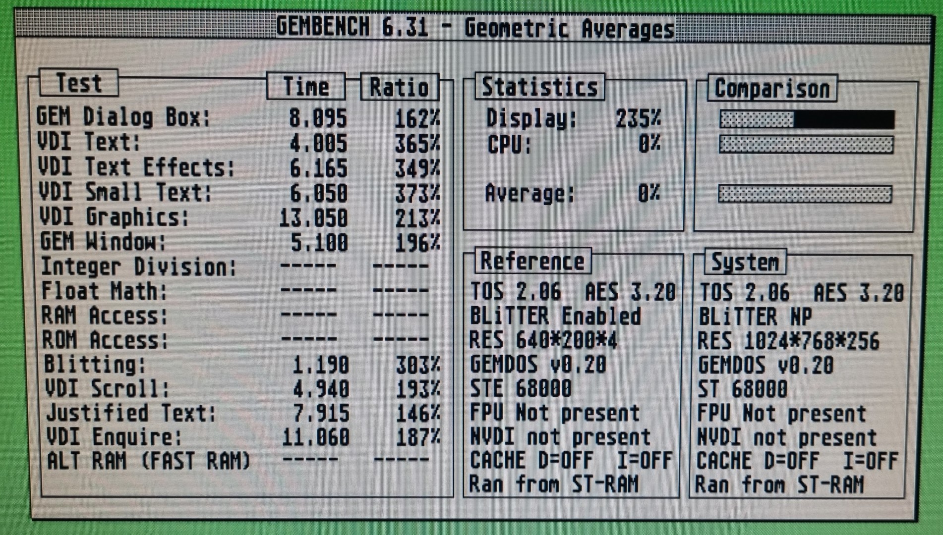
To cope with such an amount of pixels Seurat features a blitter with is able to push roughly 130MB/s for fast redraws and smooth scrolling.

As of today (July 2024) the current Gembench 6 numbers vs. 640×200 ST-Med (no NVDI!):

Transputer(s)

Yes, they might not be of everybody’s interest, but they were the main actor in the ATW800 and are fascinating beasts when you take a closer look at them.
32bit RISC’ish CPUs, running at 20-30MHz, each having 4 links to directly connect to other Transputers. That way one can create a massive, unlimited parallel system that blew away anything you could run at home back in 1990.
This strictly follows my goal #1: Historically correct. Run things on the real stuff and feel how an ATW800 felt back then.

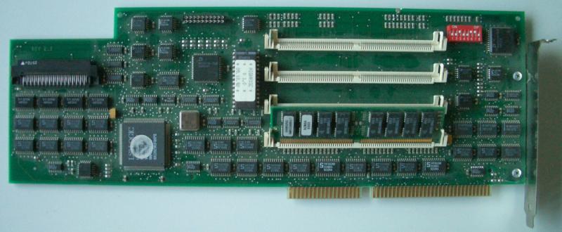
The ATW800/2 features 2 slots for classic size-1 TRAM modules next to the Nano20k. Here’s one size-2 TRAM installed:

TRAMs were/are available in many configurations, for those who want to know more, I made a dedicated page about TRAMs.

But that’s not all. Because Claus isn’t Claus without some sort of magic, he also added two synthetic Transputer cores into Seurat.
These cores are 100% T425 compatible and can not only access their own RAM (6MB, can be partitioned by the user) but also the Video-RAM… like Blossom did.
To make everything perfect, one of those synthetic Transputers has a link to the physical Transputers on the ATW800/2 which are also linked and themselves have a link at the edge of the card to connect to the outside world.

To round this up:
Everything is shared with the Atari host. You have access to the physical Transputer(s) and the synthetic ones over the 68k bus.
GEM has access to the VRAM as do the synthetic Transputers… and indirectly over their links, the physical Transputers, too.
Given proper programming, the possibilities are endless. Here are some ideas:

  • Accelerate Atari programs using Transputers (send data, let them do the math, collect results)
  • Run X windows on Helios (running the X client on a synthetic Transputer).
  • Use the synthetic Transputers as GPU. Let them do the VRAM manipulation. Lines, vertices, transformation… you name it.
Optional features

But wait, there’s more 🤓… at least for the Mega-ST:

Like I told you in the beginning, I’d like to be this as much plug-and-play as possible. So the ATW800/2 optionally features 1MB in-system programmable Flash ROM. That ROM can host 4 different versions of TOS selectable by two DIP-switches at the back-edge of the card.

Next to that DIP-switch you’ll find a dual USB port. That is a dumb loop-through to the front left edge of the ATW800/2. It is meant to connect an optional Lightning-ST so you have a nice & clean way to lead those connectors to the outside without cutting holes into your Mega-ST case.
Alternatively you can use these port to power external ACSI drives like the ACSI2SD or ACSI2STM etc.

Besides the 3 external Transputer-Links there’s also an internal one at the cards front. Just in case you have my relocator installed…

The ATW800/2 features a battery-holder for a coin battery. Because the original AA battery compartment of the Mega-ST can get in the way with the ATW800/2, this might have to be cut out 😥.
That holder can then replace the original one.

And finally, because the Nano20k has it already on-board, we’re planning to provide a harddisk interface using the Nano’s Micro-SD feature. For easy access, this is also routed to the back edge of the card providing another Mirco-SD socket. An alternative internal pin-connector is provided if you like to place the SD-card slot elsewhere.
This feature is not yet implemented but is the next on the list after VME ist running…

Why “Mega-ST” only?
Well the ATW800/2 will also be available for the VME bus, i.e. Mega-STe and Atari TT.
Most of those optional features aren’t needed in those systems. Also VME cards require a 0.5mm unpopulated edge on both sides to slide into its cage.

  • ROMs cannot fully served through the VME bus.
  • When installed in the VME cage, there’s nearly no way to feed in the USB connector of a Lightning-TT.
  • Same goes for internal TRAMs and a battery cable.
Look Ma’! VME connector fitted! (yes, its an older board revision but you get the idea)

There you have it. This is all we’re able to talk about right now. Some smaller details might change until the release – that’s called ‘agile’ 😏
Let’s sum it up again:

The ATW800/2 will be available for the Mega-ST bus as well as VME bus. This is our progress so far. It will be updated every time we think it’s worth doing so.

Mega-ST bus support
100%
VME bus support
30%
Graphics
99%
Real Transputers
100%
Synthetic Transputers
80%
4 TOS ROMs selectable and programmable
100%
Using MicroSD as harddrive
1%

Technical details

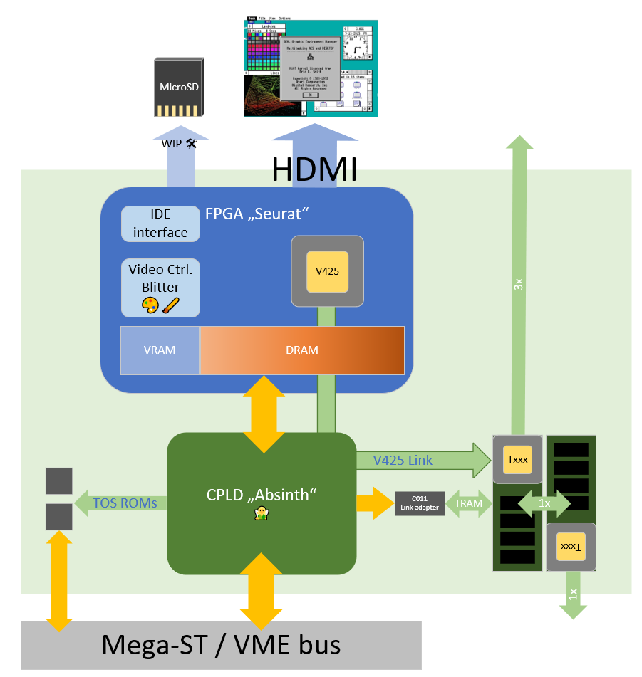
The ATW800/2 basically consists of 3 main devices:

  • The FPGA (“Seurat”)
  • The CPLD (“Absinth”)
  • The Inmos C011 link-adapter

Absinth is the glue to the system-bus. He decodes addresses, manages the different functions on the card and controls the C011. He’s also the gateway between the 5V and 3.3V worlds.

Seurat itself, the core within the FPGA, consist of the Framebuffer controller, a blitter and (currently) two synthetic T425 Transputer cores.

This is a schematic representation:

FAQ

Q: When will you release?
A: When we think it’s usable. That is at least Graphics and Transputers are at 100%.
Some minor features might be added by firmware updates later on. E.g. we consider the harddisc interface as “nice to have” but not essential as most users have at lease one HD replacement already. So that might be added later.


Q: Ok, I’m confused. How many versions will be available then?
A: As of today, we plan various levels of populating the PCB, depending on what makes sense on the specific platform – all versions have the graphics part, i.e. Seurat and Absinth and the USB loop-through connector.

The ATW800/2-VME card will be basically it. Most additional features are useless or redundant in an Atari Mega-STe or TT.

On the other hand the vanilla ATW800/2 for the Mega-ST comes with the clock-battery holder, an auxiliary power cable and will give you some options to choose from:

ATW800/2-R – added TOS ROM sockets and Flash ROMs plus DIP switch to pick one of 4 TOS versions.

ATW800/2-T – features the Inmos C011 link adapter, TRAM sockets, internal and external link connectors.

ATW800/2-RT – the full whopper 🍔


Q: If I chose not to go for a “-T” or “-R” model in the first place, can I populate those parts myself later?
A: Sure! All extra functionalities are build in Absinth already. If you’re fine with soldering and do not expect support on your additions, give it a shot.


Q: Shut up and take my money! What will it cost?
A: We’ll calculate this as soon we are 100% sure that all basic functionalities are working as expected. But according to goal #3, it won’t be incredible expensive.


Q: How will updates work?
A: As for now, Seurat (the FPGA) has to be updated via USB-C using the GoWIN Programming software (Registration required, Linux and Windows only but also works fine in VMs).
Absinth (the CPLD) needs to be updated via JTAG. This requires an Altera USB Blaster and the proper Software (part of Alteras/Intels  Quartus II IDE – 1.5GB download, registration req’d… sorry.)
We’ll provide proper documentation on this when we’re shipping.


Q: Will it work with device XYZ and/or accelerator ABC?
A: We tested the ATW800/2 with peripherals we own ourselves. That’s probably 2% of the things ever made for the Atari ST/TT – so there won’t be a guarantee that a device we don’t own will perfectly work with the ATW800/2.
That said, we will depend on your feedback and are happy to support creators of other devices to make the ATW800/2 behaving well.

As for now we positively tested the ATW800/2 against these accelerators:

    • AdSpeed
    • Turbo25

Also those devices seem to work OK up to now (more in-depth testing needed):

    • Lightning ST
    • Cloudy(-Storm)

Q: Hey, I have an idea: What about adding [enter cool feature here] !?
A: Sorry, we had hard times to even hold ourselves back from feature-creep. Actually, we think the ATW800/2 has enough features already. Some not implemented functionalities are just handled better by  already available devices .


Q: I don’t have an HDMI display, what about good old analog VGA?
A: We had to decide how to use the limited space at the external edge of the card. So the onboard HDMI of the used FPGA board was a natural choice.
If you want to use analog VGA you have to use an adaptor. Because the Nano20k does not supply sufficient power over its HDMI connector, you will als need an external “HDMI power injector” which are around 6-8€ when you’re lucky. This power injector can then conveniently fed by one of the ATW800/2’s USB ports.


Q: Why didn’t you just took a Raspberry Pi?
A: Have you read our goals? Please do so now. Thank you.


Q: Do I need a bigger power-supply?
A: It depends. If you’re still using the original power-supply of your Mega-ST this might be a good moment to replace it with something more recent.
The ATW800/2 is not tremendously demanding. With one TRAM plugged into the board, calculating Mandelbrots and displaying them in 1024×786@8bit, a 4MB Mega-ST draws 1.65 amperes in total.


Q: Can I have the source-code, schematics or gerber files?
A: Sorry, this is not an open-source project. We have to cover quite some initial R&D costs and we actually don’t like those ePay copycats.
That said, we – the extraordinary transputer gentlemen – are open for personal request in which you can explain why you need those and if there’s a convincing reason, we might share what we have.


Q: This sucks! XYZ is way better than your crap!
A: Yes, you’re right. So please move on, there is nothing to see here.

TIGA – The basic stuff

Welcome to the TIGA basics page! The fist post in my little TIGA chapter.
You probably came here because you just got (or plan to buy) a cool, shiny TIGA card and like put it to some use. Or you’ve read about it and found out, that the Web is pretty thin on that matter… Anyway, you came to the right place!

Let’s check some points fist…

Hardware

Well, if you have a card already, great, you’re set.

There were/are different versions around. The early cards used the first implementation of the graphics controller called TMS34010  which was clocked up to 60MHz (amazingly high!). For example TIs very own “TIGA Star”:

Later models used the advanced TMS34020 which started at 33MHz up to a max of 40 but had faster instruction cycle times, a faster memory interface and a twice as big instruction cache (512 bytes. Yes, bytes). Additionally the ‘020 supports the rare TM34082 floating point co-processor (actually even more than one) to speed up 3D calculation. I’m not aware of a Tool using that…

One of the first ‘020 cards was probably the Diamond from TI, which even features a socket for the FPU:

My weapon of choice is the mighty Miro TIGER:

Every TMS340 has its own RAM to run “programs” in. Depending on the model this starts at 1MB and can sometimes expanded up to 17MB. Better cards used SIMM to do this, but there were some models which used  proprietary RAM modules which are nearly impossible to come by these days.
Next the TMS340 needs VRAM, the memory holding the graphics itself. Again, depending on the model, this might vary from 1 to 4MB resulting in different max resolutions. IMHO just 1MB doesn’t do a TIGA card justice. That is just enough for 640×480 in 24bit…
Finally, as TIGA was not a standard CGA/EGA/VGA replacement, you’ll need some way of displaying the DOS text/graphics output. TIGA was always meant as an additional display mostly using a 2nd high-resolution screen, so TIGA cards either run in parallel to an existing VGA card or it also features a (mostly simple) VGA controller for this.
Very sophisticated cards like the above miroTIGER gave many options for this. It features a small VGA part (a Cirrus Logic CL-GD540 and 256K of DRAM) to make a 2nd card unnecessary or could disable that to use a 2nd card of your choice for a two-screen-solution or offered to loop-though the signal of an existing VGA card and automatically switch between them for a single-screen-setup.

Recommendation

So if you consider buying a TIGA card, go for a TMS34020 with SIMM sockets. It should have at least 1MB RAM and 2MB of VRAM. A SPEA Graphiti FGA is a good example for this minimum config.
While DRAM isn’t that important, the more VRAM you have, the better. Having a VGA controller on board might be desirable if you’re tight on slots – but to my knowledge the best VGA controller ever used on-board  was an ET4000. So it’s more or less a matter of taste.

Software

Actually this is the more important point on your list. While yes, TIGA is a standard, it contains certain proprietary parts, called the CD, GM and EXTPRIMS you’ll need to get your card going. The reason for this is the driver which is more a layer model looking like this (listed bottom-up):

Application using TIGA (e.g. AutoCAD)
application specific extensions (also *.ALM/*.RLM file)
extended primitives (EXTPRIMS.RLM/*.ALM)
Graphics Manager (e.g. tigagm.out)
Communication Driver (tigacd.exe)


The 3 yellow(ish) levels are card-dependent, so without them, you’re lost and your shiny TIGA card just makes a nice paperweight.
The lowest level is the Communications Driver, or CD for short, is 100% hardware dependent –  It is always supplied by the cards manufacturer and, well, handles the low-level communication and resides in the PC (upper-)memory.
Above that sits the Graphics Manager (GM)- this is the “real thing™”, the core or kernel of TIGA – which is the firsts thing being loaded into the cards own DRAM.
On top of the Graphics Manager sits another layer belonging to the package provided by the card manufacturer and loaded into the cards RAM, the Extended Primitives Library called EXTPRIMS.RLM in 99% of all cases. This contains all the drawing routines for primitives e.g. boxes, circles but also printing text etc. The file extension ‘RLM’ stands for relocatable load modules while ALM means absolute load modules. RLM’s are loaded and linked at run time, ALM’s are linked in advance for a fixed configuration and later at run time just loaded onto the TIGA card.

Here’s another illustration to show the layer model separated by memory regions:

With these 3 layers loaded, your TIGA card is ready to rock and awaiting commands from your application. Let’s take AutoCAD as an example – it’s probably the best example anyway as TIGA was mainly used for CAD.
It will not only load the TIGA driver but probably also some extensions provided by your cards manufacturer. So for example the miroTIGER came with a 3D-Viewer called “MulitVIEW”, ELSA provided a tool called ELSAVIEW with their Gemini cards etc.. All those tools loaded some extra code into the cards RAM (that’s the light blue layer).
All the extension tools I saw up to now didn’t require more than 200KB RAM. The TIGA core itself is at ~100KB, so for most basic stuff 1MB might suffice at first – but of course some of those tools need extra RAM for holding data so my assumption is that 2MB are a good bet to start with.

Caveats

All that said, be aware that were two main versions of the TIGA kernel – V1.x and V2.x which have slight differences in programming. Again, it depends on the model of your card which TIGA version is supported. As far as I know, V2.x (2.2 being the latest) requires a TMS34020.
ALM’s were a unique feature of TIGA V1.1 and should no longer be used with TIGA V2.0. Generally, V1.x programs do not run (properly) on a V2.x CD/GM combo.

Setup

First, most likely there might be something to setup on your card. DIP switches for example or jumpers. At least you need to know/set the base-IO address of your card. Lucky are those who have a manual 😉
Next, as this is DOS-land, there are some things to set-up in your config files. As usual with DOS, you have to set an environment variable in your AUTOEXEC.BAT:

SET TIGA=-mC:\TIGA -lC:\TIGA -i0x60
PATH=%PATH%;C:\TIGA

This defines the path(es) to your TIGA modules and libraries as well as the base-IO address, at which your card is communicating. This has to be adjusted to your hardware setting.
Also the base-path to your TIGA files needs to be in the system path.

Then you load your CD and (optionally) GM:

lh C:\TIGA\TIGACD.EXE
lhC:\TIGA\TIGALNK.EXE -LX

The 1st line is clear – if your config allows, you can load the CD into upper-memory. With the 2nd line you can pre-load the GM into the cards RAM and the -LX parameter makes sure it eXecutes right after that. This step is optional, as well programmed TIGA programs check for the GM and if it’s not loaded, they’ll take care of that.

That’s about it. Yay, your TIGA system is up and running 😀 and you’re ready for some action.

The next post shows how to program your TIGA card and do some graphics…

Myriad DASH!860

This is yet another i860 accelerator card – this time from good ol’ blighty: The Myriad DASH!860 (I’ll call it the Dash from here on) was made by Myriad Solutions Ltd. from Cambridge.

Myriad_DASH860_total

Here’s the copyright in detail:

Myriad_Copyright

What I’ve got is actually a double “sandwich” card, i.e.

  • The actual Dash card is one 16bit ISA card featuring the i860 CPU at 25MHz and its RAM consisting of 8 SIMM banks, which is connected to
  • the second ISA card is piggybacked onto the DASH!860 and is actually a graphics card using an INMOS G300 graphics controller and giving room for a maximum of 4MB VRAM – this one is called the “ShadeMASTER”

Myriad_Shademaster_total

Mhh, this setup very much reminds me of the SPEA Fire, which uses the same core parts but thanks to its higher SMD integration manages to squeeze everything onto one ISA board.

Hardware

But let’s start in the good old GeekDot tradition having a closer look at each of the cards.

The Myriad DASH!860

Here’s the left side of the Dash:

Myriad_DASH860_left

Having seen the other i860 accelerator cards, this isn’t that much different: The 64bit wide memory interface of the i860 is fed by 8 SIMM slots, each containing 1MB of RAM.
SMD parts prove that this card is a more modern design…

…while looking at the right side of the Dash shows, that its design is somewhat between the worlds:

Myriad_DASH860_right

Lots of DIL PALs has been used. Also the huge array of 8bit latches and buffers would have probably been replaced by 16bit versions later in time.
The most interesting fact in my eyes is the choice of the CPU… why did they pick the 25MHz model? The quality check on the back says 1993! In that time, 40MHz models where broadly available – maybe this was a cost reduced version of the Dash? Some sources on the web mention a 40MHz version at least.

The long pin-rows on the top- and bottom-edge as well as vertically next to the rightmost SIMM slot are the data/address lines exported to the sandwiched graphics card, called…

The ShadeMASTER

Let’s start with the left side of this card:

Myriad_Shademaster_left

Most prominent are the 16 VRAM memory ICs in ZIP package. They’re 1Mbit, so we’re looking at a whopping 2MB here.
Looking closer you’ll spot there’s room for another 16 ZIP ICs and more buffers – so the video memory can be upgraded to 4MB fairly easy (adding some more flipflops, too).
The connectors to the Dash card can be identified quite good here, too.

Myriad_Shademaster_right

On the right side of the ShadeMASTER there are a lot of PALs again – like with the DASH!860. The golden IC is an INMOS G300 graphics controller and the smaller black PLCC chip is an INMOS G176 CLUT. This one has a 6bit DAC which -theoretically- limits the ShadeMASTER to a max. of 262,144 colors (18bit). With its 2MB it could display 1024×786@16bit, or 1280×1024@8bit. With 4MB that resolution would even possible at 24bit true color…
The two transparent thingies in the top-right corner are relays to switch the video signal, i.e. there are two video (VGA) connectors at the cards edge. One 9pin input for looping in the PCs VGA signal and a 15pin output which is normally looped-through.

No signals are used on the 8bit ISA slot connector. It’s just for fixing the card in place and power-supply.

Software

While the DASH!860 seemed to be sold separately as a “general purpose application accelerator” the combination of both cards was mainly targeted at the medical 3D data visualization market.
My cards came from the Bio-Rad ThruView PLUS package which included the Dash/ShadeMASTER combo with the ThruView software.
I have a copy of the software but it’s copy-protected by a dongle, so I won’t pursue it any further (for now ;-)).
See the next chapter handling that software.

The OS – meet XNIX

What’s more important, and IMHO the most exciting fact about the Dash is the OS they run on it:
They called it XNIX. Yeah, that sounds very UNIXish, doesn’t it. A quick inspection of the kernal file shows its a i860 COFF binary and sports many POSIX calls… I was instantly hooked 😯 .

This is the parameter screen of the loader called “x.exe“:

myriad_xnix

Obviously, there are different modes to run it, depending the mode DOS is running in. As you can see, “/e” forces the enhanced-mode, while “/r” does the same with real-mode.
So either

A) you boot your DOS into real-mode by un-commenting the
device = emm386.sys
line. But leave himem.sys in there. (This will provide XMS RAM access, which is needed by XNIX)

or

B) Try running “X.EXE” with the “/r” switch.
It still might not work, as I found this line in the binary-code:
A DASH!860 E or J card is required for ‘real mode’ operation” – most likely a Revision Code.

The most interesting and useful switch is “/d” to get the 2 pages of debug output:

X01

X02

This gives you some crucial information:

  • General resources of your PC
  • Your DASH!860 capabilities
  • The I/O port used (0x160)
  • The shared memory area (0xD0000, 64KB up to 0xEFFFF)
  • Kernal size and location

In [standard] mode, I get this screen afterwards:

SCREEN01

That’s a bit puzzling, as it seems to not using XMS RAM.
Also, this shows an evil behavior: “X.EXE” will wipe your “\tmp” and “\usr\tmp” folder… unasked. Yikes!  👿

For now, I have no clear idea, how to load an i860 binary to XNIX. In another paper I found these lines:
“The i860 runs a Unix like operating system called Xnix. This is a Terminate and Stay Resident utility which allows many standard Unix applications to be executed on the i860 whilst the PC is running MSDOS. Xnix sleeps until a Unix development tool or the i860 requires servicing whereupon it wakes up and performs the required service.”

This hints towards a library to be compiled into a DOS executable, which calls XNIX kernel services.
I will have to disassemble some of the ThruView binaries and see, if thera are some calls in there which might support that theory (See the ShadeMASTER chapter below).

Config file

XNIX has a central config file. Having a look into it, it shows this:

[real]
kernel=C:\TVPLUS\kernel
stub=C:\TVPLUS\rstub.exe
startup=C:\TVPLUS\startup.rmx
translate={txt;doc}
bus=

end

The called binaries are 66% clear yet:

  • kernel is XNIX itself – ~200KB in size
  • startup.rmx is the bootstrap code for the real and standard mode.
  • stub (a DOS executable) – not totally sure. An included (compiled) BAT file calls this after “x.exe”, using the ThruView x86 binaries as parameters. Maybe a loader of XNIX/COFF binaries ?

But going through the kernel binary’s strings, there’s much more to configure:

Possible sections:

  • [enhanced]
  • [standard]
  • [real]

Pretty clear, aren’t they? DOS enhanced/real-mode setting and a section valid for both. Then there are plenty keys to fiddle around with:

387faults=
A20lock= global
Break=
HZ= %ld
SMA= %lx (NOTE: Shared Memory Address. Use '/s' for an output)
SysRq=
^C=
addressing=
bus=
cache= compaq (From the code: "The option 'cache=compaq' has been superseded by the supplied driver. Use the option: 'cache=c:\usr\860\lib\compaq.drv'")
checksum=
comms=
dashsize= /* Memorysize of the DASH!860*/
debug=
diskcache=
dma= %d
environ=
exe860=
extended=
fixA20=
floppy=
himem= /* how much XMS RAM to be used by XNIX */
hirestimer=
ioaddr=
kernel= %s
membot=
meminstalled=
memtop=
real=
reloadkernel=
shadow=
startaddr= %x
startup=
stderr=
stub=
tmpdir=
translate=
video=
watchdog=
window=
xargs= %c

ShadeMASTER

Decompiled content of “runtv.exe”:

SM_MODENAME=mode false800x600
SM_MODEFILE=C:\TVPLUS\MODE
XCNF=C:\TVPLUS\XNIX.CNF

c:\tvplus\x/r/q
c:\tvplus\rstub c:\tvplus\___tv1
c:\tvplus\rstub c:\tvplus\___tvr
c:\tvplus\x/u/q

Not an elegant way using absolute paths and hiding trivial calls in an .EXE file, but getting over it, this helps to understand the start process in further investigations.

The ShadeMASTER card uses a config-file itself, the provided one is called “mode” and contains:

[mode false800x600]
true_colour=false This is the Kosher one for 35kHz scan rate
line_length=1138
hresolution=800
vresolution=1200
hsync=142
vsync=4
hbackporch=120 <-This parameter may require tweaking for centralising
vbackporch=40 the image on some monitors
transfer_delay=18
clock=5
mem_init=1006
short_display=76
broad_pulse=130
sync_to_VGA=true
set_G300_sync=true
eight_not_six=true
overlay_mode=0
overlay_mask=0xff
palette=1
pixel_mask=0xff
line_start=0
top_of_screen=0
interrupt=false
vga_palette=false
shadow=false
delay=0x600

Many of these keys are very common with most INMOS G3xx devices e.g. the IMS B020.

To be continued…

miroHIGHRISC & miroTIGER

This is indeed a very rare breed – I was informed that less than a 100 of those were sold. Built in the end of 1992 as “Project Zorro” by the German company miro (bought by Pinnacle in ’97) it took the same line as all the other accelerated graphic cards in those days: Highspeed graphic -mostly TIGA- plus some speedy general purpose CPU. The SPEA cards using Intels i860 were direct competitors for example – I was also told that miro also looked into using the i860 but scrapped that attempt in an early stage in favor for the HIGHRISC.

The Miro HighRisc -or miroHIGHRISC as they wrote it back then- was a full-length 16-bit ISA card containing a MIPS CPU and a maximum of 32MB of RAM.

Technical facts:

  • 33MHz LSI LR33050 CPU which is a R3000 clone including the R3010 FPU minus MMU
  • 1k data- and 4k instruction caches on-die
  • 33 MIPS / 33 MFLOPS
  • 8-32 MB RAM plugged into up to 4 SIMM slots
  • 32 bit bus to connect the miroTIGER graphics card (100MB/s)
  • 2D: 150000 Vectors/s of 10 pixels length
  • 3D: 10000 triangles/s of 100 pixels, flat-shaded
  • 6000 triangles/s of 100 pixels, Gouraud-shaded

miro claimed that the HighRisc would deliver nearly twice the performance of an i860/33 solution with “real-world” applications (namely AutoCAD 12). That has yet to be proven but sounds reasonable given the limitations the i860 had when used as general purpose CPU.

Here’s the HighRisc in its full glory:

HighRiscTotal

Interestingly, there’s next to none information on the Web about this card. Probably due to its high cost (5700DM) and the failing TIGA standard.
Here’s a nice snippet from an interview (in German) from 1999 with the original product manager Frank Pölzl:
Q4. What was your biggest flop?
miroHIGHRISC, a 3D-graphic card with MIPS and TI-Graphic-Processor.

Another tasty detail is that according to a news-snippet from the German magazine c’t (12/99, p.22) this card was developed in cooperation with Silicon Graphics (SGI) which bought MIPS some years before. Maybe this was SGIs first and last attempt to get a foot into the PC market?
Yet another interesting fact: The LSI 33k CPU was later radiation hardened by a company called Synova Inc., rechristened as “Mongoose V” and as such traveled into space several times… even to Pluto!

Here’s the left side of the card in more detail. It contains the CPU and the BIOS (32k EPROM dump available here) lots of 74-logic ICs, GALs and some MACH PLDs.
At the top-left corner of the picture below you see the connector to the miroTIGER, a TIGA graphics card described a bit further down on this page.
Also, there’s  an undocumented 20-pin connector at the upper-right edge of the card. This might be the 16MB/s interface “to connect peripherals like laser printers or repro-devices” as mentioned in the c’t article. Thinking about it – it’s an interface to an UART. This will be a nice project to do further investigation.

The pinout (the connector is rotated 90° clock-wise):

GND  oo  /WR0
D0   oo
      INT2
D1   oo  /RD
D2   oo  /IOSEL
D3   oo  (unknown)
D4   oo  A2
D5   oo  A3
D6   oo  A4
D7   oo  A5
VCC  oo  A23

HighRiscLeft

The right side of the card is dominated by the 4 SIMM slots which, according to the manual, support up to 8MB each. Also there’s a DIP-switch for setting up the address-range etc.

HighRiscRight

Even it has nothing to do with MIPS, the accompanying graphics card miroTIGER fits in quite good here. This card was meant to run for itself or accelerated by the above described miroHIGHRISC. This is what it looks like:

TigerTotal

Following the TIGA standard it naturally features a TMS34020 graphics processor. This processor has its own RAM to do all the calculations, display-lists and fonts. Because TIGA was completely incompatible to the usual CGA/EGA/VGA standards you had to have such a card installed in parallel to see all the DOS/Windows outputs before switching into TIGA-mode. The normal setup was to have a 2nd high-res (1024×768++) monitor connected to the TIGA card then.
More advanced cards like the miroTIGER also had a VGA chip on-board, which saved you a slot and all the extra hassle. So let’s have a look at the details:

TigerLeft

This is the left side of the card. The nice golden chip is of course the TIGA processor. Next to it there’s a National Design V2000 chip – most probably an ASIC doing all the RAM handling and stuff.. accidentally I stumbled across a notion of a “National Design Volante2000” TIGA card. Smell the relation here? So my most recent assumption about this is, that’s a somewhat standard TMS340 glue-chip, licenced by National Design to other TIGA card manufacturers.

The SIMM above is 8MB of RAM for the TMS340. Depending on the PAL (labeled 2004, 2044 or 2084) on the lower edge of the card, one could use 0, 4 or 8MB of RAM.
On the upper left corner is the connector to the miroHIGHRISC card as well as an impressive row of DIP switches.

TigerRight

The right side is mainly occupied by 4MB VRAM for the TMS340 as well as the TI RAMDAC in the upper right corner.
Below is a very simple onboard VGA controller by Cirrus Logic (CL-GD5401 aka Acumos AVGA1) and next to it its puny 256k DRAM – which is the maximum a GD5401 can address by the way :-/

This is a good place to post a big thank you to Peter Huyoff – the wonderful guy who saved my life while doing the ‘research’ on this card.
As you might spot in the picture above, there’s one chip broken… a tiny 74AS74 flip-flop – try to find a single SMD AS74 these days. It’s impossible if you’re not prepared to pay $50 b/c of minimum order fees! And no, an F74 doesn’t do it, it’s still too slow. Been there, done that.

Peter provided me another working miroTIGER for free! That’s the spririt between real men! And Peter is definitely one of them!

The SPEA cards

Between 1990 and 1995 the German multimedia-card manufacturer SPEA was one of the leading companies in this sector (When ATI was comparably small and NVIDIA not even founded).
They offered a wide range of display-cards, from a simple ET4000 up to very expensive CAD/CAM cards using various graphic chips like the TIGA controllers, Hitachi ACRTC, Weitek, S3, 3DLabs and… of course the i860.
Later SPEA was bought by Diamond Multimedia and some employees started their own company to finalize the graphic chip they already started to design when being with SPEA (read more here… article in German, sorry).

Two SPEA cards using the i860 were built. The first was the

SPEA Fire

SPEA-Fire

This full-size ISA card features a 33MHz i860 with 4MB own RAM as well as 2MB VRAM. An Inmos G364 graphics controller is in charge for creating a picture on the monitor – BTW that’s the last and fastest graphics controller which was manufactured by Inmos.
Theoretically, this card could be called an INMOS B020 on steroids.

As this is “just” a 3D subsystem, a standard VGA was still needed for all 2D stuff. Its video signal was then looped-through the SPEA Fire… just like the Voodoo cards did it some years later.

A recent photo I’ve found on ePay shows, that there was a proprietary memory expansion available, which has to be plugged next to the i860. Probably expanding the RAM to 8MB, which can be considered as an quite serious amount of RAM back in those days.

SPEAFire_RAM_upgrade

Interestingly the manual briefly touches the possibility to be programmed with own applications using Intels APX system. Sad enough, the APX is not included on the driver disks and was sold separately for a lot of money.

FGA860

SPEA-FGA860

The FGA860 is the bigger brother of the SPEA Fire. Actually it’s two boards sandwiched together: The one on top is -again- called the Fire-Board. But this time it is designed completely different. There is no RAMDAC or such… just the i860, RAM (16MB) and some custom- and bus-logic.
Behind this, there’s a full-blown TIGA card called FGA-4E, using a TMS34020/32Mhz with 4MB DRAM and 2MB VRAM. Not so usual is the also included VGA part on the FGA-4E. This way you can save an ISA slot for the needed VGA card.

The Fire-Board was available for 5700 German Marks, the FGA-4E added another hefty 10.820 Marks making a total of 16.520 Marks (1990/91 that was about US$ 8000)!
But for that money you got a “graphic subsystem” which was capable of 300.000 2-D vectors/s (10 Pixel long) and amazing 30.000 gouraud-shaded polygons/s (10 × 10 Pixels).
[Back then, that really was amazing… today every mobile phone might be better in 3D. Here are some numbers for comparison/amusement:
3DLabs GLINT 300SX: 500.000/300.000]

Here’s a view from the top… not really much to see. It’s very hard to pry those cards from each other. I guess, they were never intended to be separated again.

SPEA-FGA860_sandwich

If you are in need of the drivers, I make them available here. It’s the IMHO most recent version from August 1994 including an AutoCAD 13 driver update.