Tag Archives: hack

UMAX tuning

Apple Performa and PowerMac models 5400/6400 used a mainboard code-named “Alchemy“. The same board, sometimes with some changes, was used in different Mac clones like the UMAX Apus 2000 & 3000 series (SuperMac C500 & C600 in the US) and PowerComputing PowerBase.

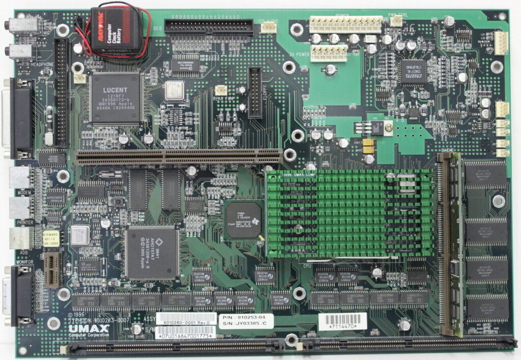
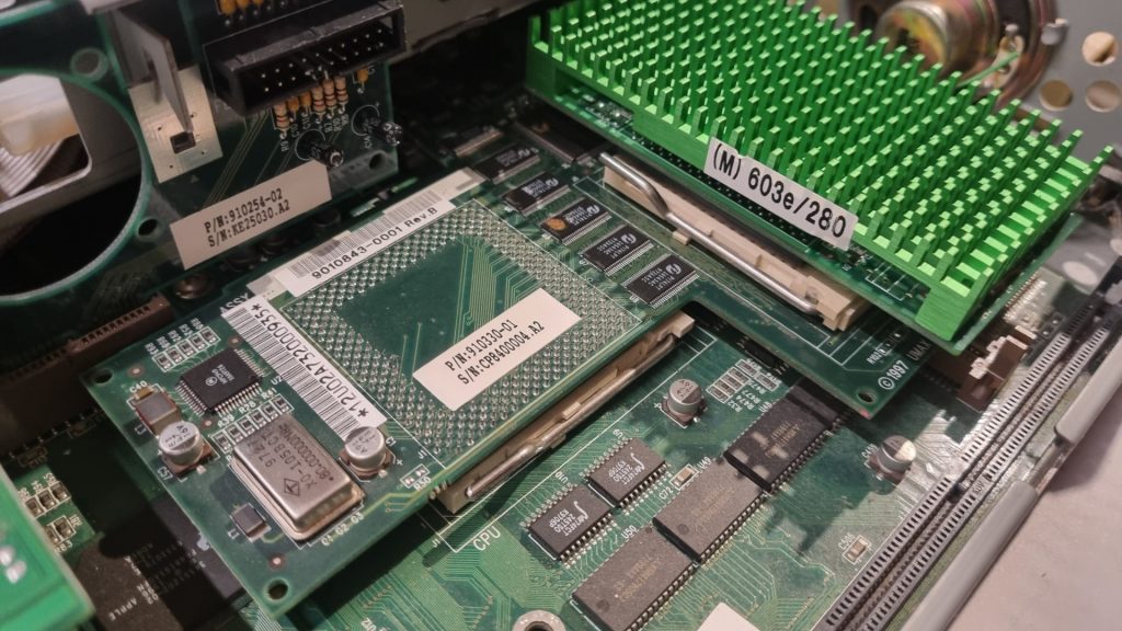
One fine day I got an UMAX Apus 2k, which uses a derivate of this board, re-cristened to “Typhoon” which you can see here in it’s full beauty:

Processor
  • Apple: PowerPC 603e
  • Power Computing: PowerPC 603e, 750
  • Umax: PowerPC 603e, 750
Only Power Computing and Umax can be upgraded
Systembus 40 MHz fixed
L2-Cache Slot for 256k or 512k L2-Cache
RAM 5V DIMM 168 Pin 60 ns (EDO)

  • Apple: 2 DIMM-Slots, 8MB on-board (136MB max.)
  • Power Computing: 3 DIMM-Slots (160MB max, Bank 1 only 32MB, Bank 2&3  64MB)
  • Umax: 2 DIMM-Slots, 16MB on-board (144MB max.)

To the limit!

So being the way I am… I had to optimize it. Jus can’t help it 😉
Here are the steps I’ve taken – in the order of making sense the most and being less difficult:

RAM

Simple rule: The more, the better.
This will get you the maximum performance – not in speed, but you can run memory-hungry applications without swapping (virtual memory) which is a major PITA and drags down everything.
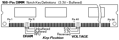
That said, finding the correct RAM is also a pain because this board uses now very obsolete 5V buffered 168-pin DIMMs. 5 Volt is already hard to find – but the buffered version is even worse.
You can check that by looking at the coding keys (“groves”) at the DIMMs bottom:

The UMAX/SuperMac board can handle two 64MB DIMMs… if you can find & afford them.

L2 Cache

A “Level 2” cache is a must-have on all PPC machines. AFAIK UMAX/SuperMac did not sell their clones without one – Apple certainly did.
If your machine doesn’t have one, get one ASAP!
If you can get a bigger one than the one you have, do so!

  • None to 256K – increases CPU performance about 30 %
    The overall responsiveness is dramatically increased
  • 256K to 512K – adds about 20% performance.
  • 512K to 1MB – need this SIMM! Mail me 😉

Umax offered an optional CacheDoubler PCB plugging between the  socket and the CPU. It features an 1MB L2-Cache and upped the bus-clock to 80 MHz. AFAIK it came as standard in the UMAX C500x/C600x models.
Of course these are unicorns now and rare as chicken teeth.

NB: There are some caveats about the L2 cache discussed further down…

Faster CPU

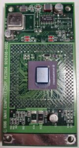
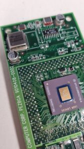
Yes, this board has a ZIF socket like the Pentiums did back then. And as such, you might be able to find a faster one. But unlike the Intel CPUs, these come on a small board covered by a big, green heat-sink.
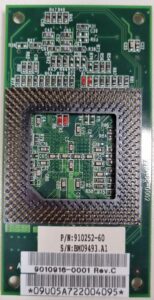
Underneath is the CPU (in BGA package) a bit of logic, caps, lots of resistors and an oscillator.

So even if you were unable to find a faster CPU you can still ‘motivate’ yours – read: Overclocking!

As usual with overclocking, every CPU has its limits. The experiences with the 603e(v) used by UMAX are:

  • 160Mhz to max. 225
  • 200Mhz to max. 240
  • 240Mhz to max. 270

How’s that done? Quite simple (if you’re ok with soldering 0603 SMD parts) by relocating some of 8 resistors which are on the top and bottom of the CPU card… marked red on the pictures below:

Use this table to change the CPU multiplier relative to the standard 40MHz bus-clock. There are also settings for 80-140MHz, but this is about overclocking so these make no sense whatsoever, right?

CPU Speed
160MHz
180MHz
200MHz
220MHz
240MHz
Busclock x
Multiplier
40 x 4
40 x 4.5
40 x 5
40 x 5.5
40 x 6
R1 [1.0k]
R2 [1.0k]
R3 [1.0k]
R9 [1.0k]
R6 [1.0k]
R7 [1.0k]
R8 [1.0k]
R13[1.0k]

Resistor color: Green = Bottom, Red = TOP
✔ = set, ❌ = not set

If the multiplier is not enough, you can also increase the bus-clock, too.
That way you can go up to a theoretical maximum of 300MHz 🔥

Oszillator 40.0MHz 45.0MHz 48.0MHz 50.0MHz
x4.0 160MHz 180MHz 192MHz 200MHz
x4.5 180MHz 202.5MHz 216MHz 225MHz
x5.0 200MHz 225MHz 240MHz 250MHz
x5.5 220MHz 247.5MHz 264MHz 275MHz
x6.0 240MHz 270MHz 288MHz 300MHz
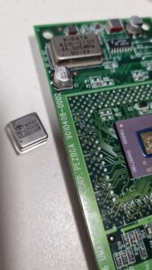
As with the resistors, you’ll need some (de)soldering skills… but it’s a simple procedure: Old oscillator out, new one in. They were even kind enough to plan for a bigger oscillator case.
Before…
…and after.

For maximum bus-performance don’t use odd divisors like “x4.5”

☝ If you plan to overclock your bus to 50MHz or more you have to get a faster L2 cache…

Most 256K cache SIMMs seem to have an IDT7MP6071 controller using an IDT71216 TAG-RRAM which has a match-time of 12 ns (You can derive that from the marking “S12PF”” on the chip). That`s far too slow for 50MHz bus-clock. If you would be able to change the TAG-RAM to a 8 ns Part, it would probably work.
Bigger cache SIMMs seem to feature faster TAG RAMs. Here’s a nice thread on 68kmla.org on those SIMMs.

Finally, here’s a comment from an Motorola engineer referring to the Tanzania board (but same issue) I found in a corner of the web:
One final problem is the main memory (DRAM) timing. If the firmware still thinks the bus clock is 40 MHz (25 ns), it won’t program enough access time (measured in clocks) at 50 MHz (20 ns). There are resistors to tell the firmware what the bus speed is, so that it can program the correct number of clocks into the PSX/PSX+ to get the required 60 ns access time. For the StarMax, this means removing R29 and installing it in the R28 location for 50 MHz operation.”
I have no clue (yet) if and where those resistors are on a Typhoon board.

Conclusion

So, what have I done in total?

I added as much RAM I was able to find (16MB on-board, one 16MB and one 32MB DIMM) to get a total of 64MB which is just OKish for a PPC Mac

I wasn’t able to (yet) find any bigger or faster L2 cache than the 256KB I already had installed. So that one stayed as-is.

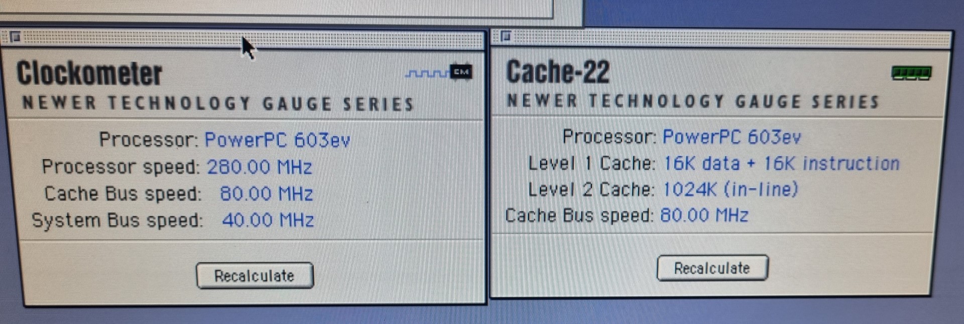
I replaced my stock 200MHz 603e CPU with a module containing a 275MHz 603ev (Even the label says 280). It has its multiplier set to 6 already… so running on a 40MHz bus is runs at just 240MHz.
My wild guess is that it was meant for the CacheDoubler mentioned above and switched to a multiplier of 3.5…
So I upped the bus-clock oscillator to 45MHz resulting in a 270MHz clock – 5Mhz below the CPUs spec but the bus is not stressed too much… the system runs stable and I measured a comfortable 45°C/113°F on the heat-sink.

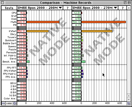
Here’s a Speedometer 4.02 comparison of before and after:

This shows that every CPU benchmark ran more or less those 35% faster, which are the difference of 200 vs 270MHz – even the Disk and Grafics performance increased between 7% and 10% which is also due to the increased bus-speed.

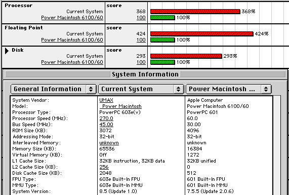
How does that fit into a greater perspective? Let’s compare to the Macbench numbers provided by user Fizzbinn in the 68kmla forum:

My system sorts itself 29% above the 240MHz machine concerning CPU performance… but FPU is less?!? No idea why that is.
Disk is probably a faster model than mine (WD Caviar 21600).

Carrera in an SE/30 – the code part 3

Ahh, back in cosy main: – looks much easier now after that crazy MMU stuff in the previous part, right?

The next subroutine called is proc32. In the complete source code (reminder: Available at GitHub) I commented that with “works (get some RSC strings)“… and well, that sums it up pretty good.
proc32 loads (i.e. creates handles) from the resource-fork, e.g. the icons used in the menu-bar and several error-messages like “This application must run on the 68030 processor, please quit all other 68040 applications and re-run this application.“. That’s it. Boring…
That boredom instantly changes when we get to the next subroutine proc43located at 0x29DA…

I did it my way…

One fascinating thing about classic Mac OS is how easy it is to patch system calls, aka Toolbox traps. For example in the previous post we came about _BlockMove, which is a Toolbox call to copy an amount of RAM from A to B.
For example you have just read this article about a faster BlockMove method, you’re totally free to patch (read: replace) _BlockMove with your speedier version and automatically use this throughout your application – or even system-wide, if you’ve created an INIT…  [If you want to know all about it… here’s a book for you]

And that’s what proc43 heavily does. Because it’s a long subroutine (230 lines) so I will give you just one example – the inline comments should do…

2BE2:        MOVE    #$A02E,D0     ; BlockMove
2BE6:        _GetTrapAddress newOS ; (D0/trapNum:Word):A0\ProcPtr 
2BE8:        MOVE.L  A0,$270(A5)   ; oldBlockmove
2BEC:        LEA     data42,A0     ; myBlockMove
2BF0:        TST.B   MMU32bit      ; loMem global "current address mode"
2BF4:        BNE.S   lae_70        ; skip if 32bit clean machine else
2BF6:        LEA     data43,A0     ; use a different entry for dirty machines
2BFA: lae_70 MOVE.L  A0,$274(A5)   ; save routine pointer to $274(A5)	
2BFE:        LEA     data41,A0     ; DC.L 0000 0000
2C02:        MOVE.L  $270(A5),(A0) ; save oldBlockmove vector into there
2C06:        MOVE.L  #$A02E,D0     ; BlockMove
2C0C:        LEA     data40,A0     ; aaaand replace it by myBlockmove
2C10:        _SetTrapAddress newOS; (A0/trapAddr:ProcPtr; D0/trapNum:Word)

This is the sum up what else being done:

  • Save all debugger vectors into A5-world locations (suspicious. I sense Macsbug killing…)
  • Load the PACK4 resource, that’s the Floating Point emulation package (aka SANE) if no FPU found
  • Check & read several system Gestalt codes into A5-world (0x2AAC-0x2B44)
  • Patch several Toolbox traps
    • SwapMMUMode replaced by data19
    • VM_Displatch by data22
    • Pack4 by data10
    • Pack5 by data11
    • BlockMove by data40
    • jClearCache by myClearCache
    • GetNextEvent by myGetNextEvent
    • GetResource by myGetResource
    • SCSIdispatch by mySCSIdispatch
    • DrawMenuBar by myDrawMB
    • LoadSeg by data31
    • UnLoadSeg by data32
    • HWPriv by data33
    • vStdExit by data34

So far, so many.  Then there’s some RAM copying going on, of which I’m currently not quite sure what it is good for (0x2CAC-0x2CD8) 💡 .

Finally, the myShutdown routine is installed into the Shutdown Manager, i.e. it will executed before the Mac is powered down/restarting (it simply switches the host back to its own 68030). After that, RTS into main…

“There and back again…”

Barely back in main, a JSR 12(A6) warps us into MacII_4th, the last of the four handlers every supported system has.

This loads specific data from the FPSP into RAM (namely IDs 0x12C and 0x12D).
Finally a special floppy driver is installed (myFloppyDrvr @ 0x954) which IMHO just differs from the original in handling the ‘040 caches correctly. That was that and back to main…

The next sub-routine in line is chkATalkVer. I can rightfully name that routine because it’s short and crystal clear: Figure out if AppleTalk is installed, and if true, return its version in D0 (and also write it into A5-world). C’est ca…

This is the end…

It’s getting ugly (for now)… proc42 will be called – the last subroutine in main before my SE/30 crashes and burns  😥

The first few lines (0x28F4-0x293C) are comparably harmless. They are working around a bug in System 7.1 which was corrected in 2/17/92 according to some dark sources (“Corrected value of timeSCSIDB from 0DA6 to 0B24”).
After that, proc38 (0x293C) is called which again calls proc39 and something’s done with the TimeManager, not really sure what’s exactly going on, but it feels like a timing-benchmark heavily using InsTime, PrimeTime and RmvTime Toolbox calls.

[hold yer breath] Then we’re getting closer to the flat line… The stack is filled with these parameters:

2940:   CLR.L   -(A7)       ;PUSH.L 00000000 
2942:   CLR.L   -(A7)       ;PUSH.L 00000000 
2944:   CLR.L   -(A7)       ;PUSH.L 00000000 
2946:   PUSH.L  #$80008000  ;       80008000
294C:   CLR.L   -(A7)       ;PUSH.L 00000000 
294E:   PUSH.L  #64         ;       00000040
2954:   PUSH.L  #1          ;       00000001

and SpeedProc is called…

…To be continued 😉

P.S: I changed course (again) and started to investigate more into the C040’s hardware. The more I understand of the INIT/CP workings the more I can’t fight the idea that it really might be a hardware timing issue.

Carrera in an SE/30 – the code part 2

3rd handler

Next up is the 3rd handler, MacII_3rd: (0x3F94) in our case. Actually it’s called with JSR 8(A6), but that’s an 8 byte offset to the ‘base-address’ of any handler. Clever stuff, huh (Google for ‘pointer-table’)?

This subroutine contains serious magic and was a real hard nut to crack. Especially because it tricked me into believing that I’ve found the ‘crashsite’… which, to spoil the tension, isn’t.
It just kept on killing  Macsbug, because it’s so low-level.

What this routine does is replacing the Vector Base Register (VBR) which ‘lives’ at address 0x00000000. Evil stuff.

  • After disabling interrupts and switching to 32bit-mode a field with 6 long-words (data107) will be populated with data generated in other routines.
    For now I can only guess what these entries are (Values from my SE/30 given in brackets). We’ll discuss all that further down.
  • 0x3FC6 to 0x3FD8 calculates the size of the chunk of code starting at data106 (0x4008) to the beginning of MacII_4th (i.e. the end of Mac_3rd), which is 180 bytes.
  • Using this length, the routine first saves the current VBR onto the stack using the system call _BlockMove.
    Then the original VBR (+some more) will be replaced by the new version beginning at data106. (Killing Macsbug – more on that later)
  • BSR 53_cmd_1x is been called. This brings the Carrera040 into life most likely using the just copied VBR (This is discussed in much detail further down).
  • Now the contents of the stack (= copy of the original VBR) will be copied back into its place, this time using a classic DBRA loop (0x3FF4). My guess, no Toolbox call possible at the moment.
  • Adjust the stack, back to 16bit mode, restore Registers and return-from-subroutiene. Done.

Here’s the code doing all this:

3F94:MacII_3rd: MOVE    SR,-(A7)     ; 3rd call from MacII handler
3F96:           ORI     #$700,SR       ; Set bit 9-11 of SR (disable Interrupts)
3F9A:           MOVEM.L D0-D2/A0-A2,-(A7)
3F9E:           MOVEQ   #1,D0
3FA0:           _SwapMMUMode  
3FA2:           PUSH.B  D0
3FA4:           SUBA.L  A2,A2         ; faster movea.l #0,a2
3FA6:           LEA     data107,A0    ; Filling the data into the 6x32 field
3FAA:           MOVE.L  96(A5),D0
3FAE:           MOVE.L  D0,(A0)+      ; SE30: 9FE00
3FB0:           LEA     data69,A1
3FB4:           MOVE.L  A1,(A0)+      ; SE30: 9D6E2 (User/Supervisor Rootpointer?)
3FB6:           MOVE.L  $64(A5),(A0)+ ; 807FC040
3FBA:           MOVE.L  $6C(A5),(A0)+ ; 807FC040
3FBE:           MOVE.L  $68(A5),(A0)+ ; 00000000
3FC2:           MOVE.L  $70(A5),(A0)+ ; 00000000
3FC6:           LEA     MacII_4th,A0
3FCA:           MOVE.L  A0,D2
3FCC:           LEA     data106,A0
3FD0:           SUB.L   A0,D2         ; 'distance' from data106 to MacII_4th
3FD2:           SUBA.L  D2,A7
3FD4:           MOVEA.L A2,A0
3FD6:           MOVEA.L A7,A1
	  	; save the current VBR to the stack
3FD8:           MOVE.L  D2,D0
	  	; A0 = SE30: 00000000 (src)  - IIci: $FBB08000
	  	; A1 = SE30: 027ff34c (dest) - IIci: $3BF9FC6
	  	; D0 = B4    (count)   - SAME on the IIci!    
3FDA:           _BlockMove ; (A0/srcPtr,A1/destPtr:Ptr; D0/byteCount:Size) 
	  	; write my own VBR...
                ; This copies 180 bytes into 0x000000000 replacing the original VBR. 
                ; ... and kills Macsbug if not circumvented properly.
3FDC:           LEA     data106,A0
3FE0:           MOVEA.L A2,A1
3FE2:           MOVE.L  D2,D0
	  	; A0 = 9F900 (src)   - IIci 10C4EA (data88)    
	  	; A1 = 00000 (dest)  - IIci FBB08000
	  	; D0 = B4    (count) - IIci same  
3FE4:           _BlockMove ; (A0/srcPtr,A1/destPtr:Ptr; D0/byteCount:Size) 
3FE6:           BSR     53_cmd_1x  ; Bring the C040 to life
3FEA:           MOVEA.L A7,A0  ; SP to A0
3FEC:           MOVEA.L A2,A1  ; SE30: 00000000
3FEE:           MOVE.L  D2,D0  ; the code length (B4 again)
3FF0:           BRA.S   lae_163
3FF2:   lae_162 MOVE.B  (A0)+,(A1)+ ; Write the VBR back from the stack
3FF4:   lae_163 DBRA    D0,lae_162
3FF8:           ADDA.L  D2,A7 ; adjust the stack
3FFA:           POP.B   D0
3FFC:           _SwapMMUMode  
3FFE:           MOVEM.L (A7)+,D0-D2/A0-A2
4002:           MOVE    (A7)+,SR
4004:           MOVEQ   #0,D0
4006:           RTS     
 
; Start of VBR replacement- and 040-Code being copied to 0x0 the by line 0x3FE4 
; /if/ theses are the Vectors 0-17, then their meaning would be:
 
4008: data106:  DC.L    #$00001000 ; Reset initial Stack Pointer
400C:           DC.L    #$00000050 ; Reset initial Program Counter
; - ALL of these Vectors point to addr 4050 (offset 0x48) -
4010:           DC.L    #$00000048 ; Buserror  
4014:           DC.L    #$00000048 ; Adress Error
4018:           DC.L    #$00000048 ; Illegal Instruction
401C:           DC.L    #$00000048 ; Zero Divide
4020:           DC.L    #$00000048 ; CHK, CHK2 instruction
4024:           DC.L    #$00000048 ; cpTRAPcc, TRAPcc, TRAPV instruction
4028:           DC.L    #$00000048 ; Privilige Violation
402C:           DC.L    #$00000048 ; Trace
4030:           DC.L    #$00000048 ; LINE 1010 Emulation
4034:           DC.L    #$00000048 ; LINE 1111 Emulation
 
; THESE are definitely no vectors, they are dynamically written by the code above
; and to be used to setup the 040 MMU registers.
4038: data107:  DC.L    #$0009FE00 ;  
403C:           DC.L    #$0009D6E2; 
4040:           DC.L    #$807FC040 ; 
4044:           DC.L    #$807FC040 ; SE30: 
4048:           DC.L    #$00000000 ; SE30: 00000000 
404C:           DC.L    #$00000000 ; SE30: 00000000 
 
4050:           CLR.L   $53000000  ; Poke 0 to $53000000
4056:           BRA     lae_164    ; This points to itself... I'm lost at the moment.
4058:           LEA     data107,A0 ; SE30: 9F900
405C:           MOVE.L  (A0)+,D1   ; SE30: 0009FE00 (User/Supervisor Rootpointer)
405E:           MOVEA.L (A0)+,A1   ; 0009D6E2
4060:           MOVE.L  (A0)+,D4   ; 807FC040
4062:           MOVE.L  (A0)+,D5   ; 807FC040
4064:           MOVE.L  (A0)+,D6   ; 00000000
4066:           MOVE.L  (A0)+,D7   ; 00000000
4068:           MOVE.L  #$C000,D0
406E$           MOVEC   D0,ITT0   ; Set Instruction Transparent Translation
4072$           MOVEC   D0,DTT0   ; Set Data Transparent Translation
4076$           MOVEC   D1,SRP    ; Set Supervisor Rootpointer
407A$           MOVEC   D1,URP    ; Set User Rootpointer
407E:           MOVE.L  #$C000,D0
4084$           PFLUSHA           ; Invalidates all entries in the address translation cache
4086$           MOVEC   D0,TC 
408A:           LEA     data108,A0
408E:           ADDA.L  #$53002000,A0 ; (=0x530A1900)
4094:           JMP     (A0)      ; JuMP to data108 code (below) in C040 RAM range?     
 
4096:  data108: MOVEQ   #0,D0
4098$           MOVEC   D0,ITT0 
409C$           MOVEC   D0,DTT0 
40A0$           MOVEC   D4,ITT0 
40A4$           MOVEC   D5,DTT0 
40A8$           MOVEC   D6,ITT1 
40AC$           MOVEC   D7,DTT1 
40B0$           CINVA   BC
40B2:           NOP     
40B4:           MOVEQ   #0,D0
40B6$           MOVEC   D0,CACR
40BA:           JMP     (A1)    ; 0009D6E2
 
; END 040 Code being copied to somewhere by line 3FE4 
40BC: MacII_4th: MOVEM.L D1-D7/A0-A4,-(A7)  ; 4th subroutine called my MacII_handler
[...]

The Vector Base Register

I wasn’t precise when I initially said “replacing the VBR”. What actually happens is that this routine uses what I’d call an interim-VBR for the moment it initializes the 68040 on the C040. You’ve probably saw the link referring to what the VBR is in the 1st post of this series, but let me go a bit more into detail.

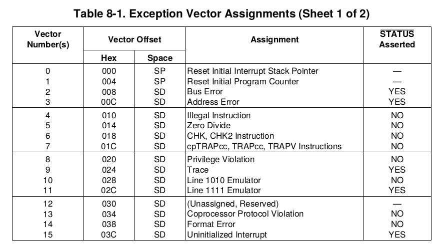
The VBR is a list of addresses (aka vectors) the CPU refers to in case of an exception – and this is true for every 68k system out there, e.g. Mac, SUN, NeXT, Amiga or Atari. Some of them might do some relocation using their MMU, but even the virtual address will be 0x00000000 and the order is the same.  There are 16 basic vectors as listed here:

If for example a divide-by-zero happens, the CPU would call a handler which address is stored in 0x14.  Pretty simple.
So let’s have a look what MacII_3rd left in the VBR (and below that) when the ‘interim VBR’ is in place:

0000: data106:  DC.L    #$00001000 ; Reset initial Stack Pointer
0004:           DC.L    #$00000050 ; Reset initial Program Counter
     ; - ALL of these Vectors point to addr 0x48 -
0008:           DC.L    #$00000048 ; Buserror  
000C:           DC.L    #$00000048 ; Adress Error
0010:           DC.L    #$00000048 ; Illegal Instruction
0014:           DC.L    #$00000048 ; Zero Divide
0018:           DC.L    #$00000048 ; CHK, CHK2 instruction
001C:           DC.L    #$00000048 ; cpTRAPcc, TRAPcc, TRAPV instruction
0020:           DC.L    #$00000048 ; Privilige Violation
0024:           DC.L    #$00000048 ; Trace
0028:           DC.L    #$00000048 ; LINE 1010 Emulation
002C:           DC.L    #$00000048 ; LINE 1111 Emulation
     ; - THESE are definitely no vectors, they are dynamically written by the 
     ;   code above and to be used to setup the 040 MMU registers.
0030:  data107: DC.L    #$00000000 ; SE30: 0009FE00  (12)
0034:           DC.L    #$00000000 ; SE30: 0009D6E2  (13)
0038:           DC.L    #$00000000 ; SE30: 807FC040  (14) 
003C:           DC.L    #$00000000 ; SE30: 807FC040  (15)
0040:           DC.L    #$00000000 ; SE30: 00000000 
0044:           DC.L    #$00000000 ; SE30: 00000000 
 
0048:           CLR.L   $53000000  ; Poke 0 to $53000000 ; C040 off
004C:  blocker3 BRA     blocker3    ; Points to itself... probably a "blocker"
0050:           LEA     data107,A0 ; initial Program Counter (SE30: 9F900)
0054:           MOVE.L  (A0)+,D1   ; SE30: 0009FE00 (User/Supervisor Rootpointer)
0058:           MOVEA.L (A0)+,A1   ; 0009D6E2
005C:           MOVE.L  (A0)+,D4   ; 807FC040
0060:           MOVE.L  (A0)+,D5   ; 807FC040
0064:           MOVE.L  (A0)+,D6   ; 00000000
0068:           MOVE.L  (A0)+,D7   ; 00000000
006C:           MOVE.L  #$C000,D0
0070:           MOVEC   D0,ITT0    ; Set Instruction Transparent Translation
0074:           MOVEC   D0,DTT0    ; Set Data Transparent Translation
0078:           MOVEC   D1,SRP     ; Set Supervisor Rootpointer
007C:           MOVEC   D1,URP     ; Set User Rootpointer
0080:           MOVE.L  #$C000,D0
0084:           PFLUSHA            ; Invalidates all entries in the address translation cache
0088:           MOVEC   D0,TC 
008C:           LEA     data108,A0
0090:           ADDA.L  #$53002000,A0 ; (=0x530A1900)
0094:           JMP     (A0)       ; JuMP to data108 code (below) in C040 RAM range? 
 
009C:  data108: MOVEQ   #0,D0
00A0:           MOVEC   D0,ITT0 ; 0
00A4:           MOVEC   D0,DTT0 ; 0
00A8:           MOVEC   D4,ITT0 ; 807FC040
00AC:           MOVEC   D5,DTT0 ; 807FC040
00B0:           MOVEC   D6,ITT1 ; 00000000
00B4:           MOVEC   D7,DTT1 ; 00000000
00B8:           CINVA   BC
00BC:           NOP     
00C0:           MOVEQ   #0,D0
00C4:           MOVEC   D0,CACR
00C8:           JMP     (A1)    ; 0009D6E2
Farewell, old friend

At this point, my SE/30 always froze and I thought this must be the point where to find incompatibilities between the IIci and SE/30.
But after understanding, what’s really going on, it was clear that overwriting the TRAP exception (Nr.7), Macsbug was simply kicked out of the game as this exception is triggered after every step/trace you do in a debugger…
So to get beyond this point, I had to modify the program counter to skip the point where TRAP is copied-over… which is done inside the Toolbox’ _BlockMove call. So I had to single-step into that and find the right call/time to do a ‘pc=pc+2’ 😉 (Good thing you can define a macro for that).

Okayyyyy. After that’s been written, 53_cmd_1x is called, presumably telling the C040 to come to life.
And keen as it is, it’ll look up the “Reset initial Program Counter” (VBR: 0xC) and starts executing code from 0x50. Any other occurring exception will call the ‘handler’ at 0x48, simply switching the C004 off and sit in an endless loop (0x4C) – probably making the 68030 to take over again.

EmEmYou!

Given everything’s fine, the code at 0x50 will start reading the previously populated data from data107 into several registers.
Then some serious 68040 MMU table setup happens – so this is some kind of ‘040 initialization routine… and the ‘040 is actually running. Woohoo!

Time for some special register explanation:
As we all know, the 68040 has two in-build 4k caches and an MMU. The latter can be programmed how and what to cache. This is defined in 4 registers of which only 2 are of interest here: ITT0 and DTT0, the Instruction and Data Transparent Translation registers, both sharing the same bit-fields following this pattern:

BBBBBBBBMMMMMMMMESS000UU0CC00W00

  • BLogical Address Base – compared with address bits A31-A24. Addresses that match in this comparison are transparently translated
  • MLogical Address Mask – setting a bit in this field causes corresponding bit in Base field to be ignored
  • E – Enable Bit – 1 – translation enabled; 0 – disabled
  • SSupervisor Mode – 00 – match only in user mode 01 – match only in supervisor mode 1x – ignore mode when matching
  • U – User Page Attributes – ignored by 040
  • CCache mode – 00 – Cacheable, Write-through 01 – Cacheable, Copyback 10 – Noncacheable, Serialized 11 – Noncacheable
  • WWrite protect – 0 – write permitted; 1 – write disabled

Here’s an example:

807FC040 = 10000000011111111100000001000000 
           BBBBBBBBMMMMMMMMESS000UU0CC00W00

which means:

  • a bit less than 2GB transparently translated (2032MB)
  • translation enabled
  • Supervisor Mode: ignore mode when matching
  • Cache mode: Noncacheable, Serialized
  • Write permitted

So let’s have a look at the code again:

At 0x70/0x74 the MMU is set to 0xC000, i.e. Enable translation, apply for user & supervisor mode, write-though cache, for logical address space 0x80000000-0x00ffffff (2GB minus the bottom 16MB).
Then Supervisor & User Rootpointer are set to 0x9FE00, then the address translation cache is flushed to finally set the Translation Control register to Enable & 8K page size (0x88)… up to here this was pretty much ‘by the book’ of how to set-up MMU tables.

Having its MMU all set, the 68040 now gets something to chew on:
The address of data108 is added to 0x53002000 and jumped to!
💡  Does 0x53002000 equal 0x00000000 for the C040?

Let’s assume the C040 executes the code at data108 for now. That is:

  • Clear the ITT/DTT registers
  • Set the MMU to 0x807FC040 (see decoding example above)
  • invalidate caches and wait’a’NOP to have that happened
  • then disable all caches
  • and jump to where A1 points to. In my SE/30 that’s 0x9D6E2, previously loaded from data107 in 0x58

Writing all this from the top of my head, I’m not 100% sure where this address is pointing to. I must be somewhat back into MacII_3rd (0x3FEA), because this is where the program execution resumes (Need to check this with Macsbug and will update).

For now, I’m tempted to call MacII_3rd something like ‘C040_MMU_setup‘… but I’d love to have this confirmed  💡 by somebody who knows more than me 😉

Next up will be continuing working further through the main: procedure again… so move over here.

Carrera in an SE/30 – the code part 1

The disassembled code of the Micromac Carrera 040 control panel is quite big: 6000+ lines of 68030/40 assembly…

While these posts might be entertaining and giving you an insight into classic MacOS driver code, they are also meant as a notebook to myself to get into the source quickly – especially after some weeks or months of distraction 😉

That said, I will not discuss each and every line of code. There are many parts which aren’t important (for now) or just not reached yet.
Still, it will take several parts/chapters to cover everything I worked on.

The complete code is available over here on GitHub and will updated every time I’m working on it.
Whenever I’m mentioning addresses I’m referring to this code on GitHub. NB: I will never use line-numbers as these might change during editing the source.
Also, when you’ll see a light-bulb  💡  somewhere, this is where I’m not sure and happy about enlightenment or comments from you 😉

This article is totally work-in-progress closed.
E.g. every now and then my theories about what a certain code does changes, I learn new things and all the sudden whole blocks of code make sense… so this post will change/grow, too.Bolle did a lot of hardware research and in the end it became clear that the INIT/Driver has nothing to do with the non-function of the Carrera in an SE/30. After Bolle modified his adapter, the Carrera 040 is happily running in my ’30 now.But still, this series of posts is definitely worth reading, especially if you’re into reverse engineering 68k assembly code.

Approaching… difficulties.

What’s the main job of this code? From a 30000ft perspective the simple answer is “switching the Carrera040 on and off”, i.e. toggling between the hosts slower on-board 68030 and the insanely fast 68040 on the C040. At boot-time… as well as during the system is running (by user interaction).

Sounds pretty simple, huh? Lowering our flight altitude to 3000ft more things come into play:
Identify the hosting Macintosh. As mentioned in the previous chapter, the C040 was able to run in a Mac II, IIx, IIcx, IIvx, IIvi, IIvm, IIsi, IIci, LC and LCII… all of them different in many places. These differences have to be handled…
Down at 30ft we have to admit that there are differences between a 68030 and his younger brother 68040, mainly concerning caches, FPU and the MMU.
Finally hitting the ground, it’s becoming clear that it is everything but trivial to halt a running processor, save its complete context and start another (slightly different) processor with that. And back again…

Some given things before we start:

  • We will concentrate on the IIx “branch” as this machine is closest to the SE/30 like not-32bit-clean, memory-map, the GLUE chip, two real VIAs with the same register layout etc.
  • I learned from the code that the C040 is memory-mapped at 0x53000000 in some of the supported models, especially the IIx and IIci. This means 32bit addressing is a must (-> need “mode32” INIT or clean ROM)
  • I tried to comment as much as possible/understood inline (i.e in the code) – a good bit of 68k machine language knowledge is still required 😉
  • If something needs more explanation, I’ll try to provide this before the code quote or afterwards.

So this is the main routine (at 0x21FC):

main     MOVEM.L A4-A6,-(A7)
         MOVE.L  D0,D7
         MOVE.L  #$31E,D0    ; need 798 bytes
         _NewPtr ,CL_SY      ; allocate requested amount of memory (D0) in system
                             ; heap (returned in A0) and initialize to zeroes
         TST     D0          ; success?
         BNE.S   lae_6       ; nope, exit.
         LEA     data2,A1    ; else
         MOVE.L  A0,(A1) ; Init A5 world and save into data2
         MOVEA.L A0,A5
         MOVE    #$A89F,D0   ; UnimplTrap
         _GetTrapAddress     ; (D0/trapNum:Word):A0\ProcPtr 
         MOVE.L  A0,$29C(A5) ; save the trap addr into 2 places 
         MOVE.L  A0,$2A0(A5) ; in the A5 world
         BSR     sysDetect   ; Jump to Machine detection routine 
         BNE.S   lae_6       ; success?
         MOVE.L  D7,D0
         JSR     4(A6)       ; We jump to the subroutine set in the detection routine
                             ; for the second time, this time offset 4...
			     ; i.e. we skip the 1st 'BRA' there
         BNE.S   lae_6       ; success?
         BSR     instFPSP    ; Install Motos FPSP
         BNE.S   lae_6       ; success?
         JSR     8(A6)       ; That's the 3rd call in the handler call cascade (needs hack for MacsBug!)
         BNE.S   lae_6       ; success?
         BSR     proc32      ; works (get some RSC strings)
         BSR     proc43      ; install traps
         BNE.S   lae_6       ; success?
         JSR     12(A6)      ; That's the 4th call in the handler call cascade
         BNE.S   lae_6       ; success?
         BSR     proc41      ; works (atalk?)
         BSR     proc42      ; VIA stuff and such - BOOM
         BSR     proc29
         MOVEM.L (A7)+,A4-A6
         MOVEQ   #0,D0

As you can see, there are 10 calls to subroutines- currently it crashes inside the 8th subroutine, currently called proc42… But let’s check these subroutines one by one.

sysDetect

This is the subroutine I had to “patch” to initially make the driver work with an SE/30. It starts at 0x2022 and does these things:

  • Check if the ‘Gestalt‘ trap is available at all (very good style!) else throw an error
  • If it is, read the machines Gestalt code into D0, throw an error if zero
  • Decide which ‘handler’ to choose given the Gestalt code.

Based on their Gestalt codes there are four groups of Macs defined in the following lines (0x204C – 0x20AC):

  • Mac II/IIx/IIcx — “dirty Macs”, not 32bit clean, no PDS
    • “Expansion I/O Space” from 0x51000000 to 0x5FFFFFFF
    •  the C040 installs with an adapter right into the CPU socket in the II/IIx/IIcx
    • SE/30 is also “dirty”, need mode32 or IIsi ROM in slot
    • these machines also use the GLUE chip to emulate the VIA2 like the SE/30
  • Mac IIvx, IIvi, IIvm — special kind of PDS slot
    • there’s no mentioning of support on the MicroMac page
  • Mac IIsi, IIci
    • Kind of interesting because the si has the same PDS slot like the SE/30
    • Uses the RBV (Ram Based Video) controller which emulates the VIA2
    • Therefore totally different memory layout (VRAM at 0x00000000 mapped by the MMU etc.)
  • Mac LC, LCII, Color Classic
    • These share the same LC-PDS slot

If your Mac is one of those (or patched at 0x2058), you’ll branch into sys_check: (0x20BA) which will make sure you run at least System 6.0.5, have virtual memory switched off and jumps into the selected handler code (address saved in A6) at 0x20EA  for the first time.

Here’s the code of what’s discussed above:

2022: sysDetect: MOVE.L  #$A0AD,D0  ; Gestalt
2028:         _GetTrapAddress newOS ; (D0/trapNum:Word):A0\ProcPtr 
202A:         MOVE.L  A0,D2
202C:         MOVE.L  #$A89F,D0     ; UnimplTrap
2032:         _GetTrapAddress newTool; (D0/trapNum:Word):A0\ProcPtr 
2034:         CMP.L   A0,D2
2036:         BEQ     OS_bad
203A:         MOVE.L  #'mach',D0
2040:         _Gestalt ; (A0/selector:OSType):D0\OSErr 
2042:         BNE     bad_conf      ; If we can't read it, fire general Error Msg
2046:         MOVE.L  A0,D0
2048:         MOVE.L  D0,2(A5)
 
; Check for several Mac models which are grouped into 3, each having its own handler routine. 
; 1) Mac II/IIx/IIcx 
; 2) IIvx, IIvi, IIvm 
; 3) IIsi, IIci     
; 4) LC, LCII, Color Classic
 
204C:         LEA     MacII_handler,A6   ; -- The dirty gang
2050:         CMPI.L  #6,D0        ; MacII 
2056:         BEQ.S   sys_check
2058:         CMPI.L  #7,D0        ; MacIIx - we replace this by the SE/30 #9
205E:         BEQ.S   sys_check
2060:         CMPI.L  #8,D0        ; IIcx
2066:         BEQ.S   sys_check
 
2068:         LEA     V_handler,A6   ; -- The "V" Macs.
206C:         CMPI.L  #48,D0       ; IIvx
2072:         BEQ.S   sys_check
2074:         CMPI.L  #44,D0       ; IIvi
207A:         BEQ.S   sys_check
207C:         CMPI.L  #45,D0       ; IIvm
2082:         BEQ.S   sys_check
 
2084:         LEA     IIci_handler,A6   ; -- IIci and IIsi
                                        ; BOTH share the same "Expansion I/O Space" (0x5300 0000)
2088:         CMPI.L  #11,D0       ; IIci
208E:         BEQ.S   sys_check
2090:         CMPI.L  #18,D0       ; IIsi 
2096:         BEQ.S   sys_check
 
2098:         LEA     LC_handler,A6    ; -- The LC-PDS family
209C:         CMPI.L  #19,D0       ; LC
20A2:         BEQ.S   sys_check
20A4:         CMPI.L  #37,D0       ; LCII
20AA:         BEQ.S   sys_check
20AC:         CMPI.L  #49,D0       ; Color Classic
20B2:         BEQ.S   sys_check
 
; Any other Model/Gestalt will bring up an error alert-box 
 
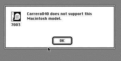
20B4:         MOVE    #$1B5B,D0    ; "Carrera040 does not support this Macintosh model."
20B8:         BRA.S   RET_err      ; -> "TST     D0 & RTS"
 
; We found a supported model, so keep on going checking for the OS version...
 
20BA: sys_check: MOVE.L  #'sysv',D0    ; Check OS version
20C0:         _Gestalt              ; (A0/selector:OSType):D0\OSErr 
20C2:         BNE.S   bad_conf      ; If we can't read it, fire general Error Msg
20C4:         MOVE.L  A0,D0
20C6:         CMPI    #$605,D0     ; System 6.0.5
20CA:         BGE.S   OS_ok        ; or greater
20CC: OS_bad: MOVE    #$1B5C,D0    ; "Carrera040 does not work with this version of the operating system."
20D0:         BRA.S   RET_err      ;
20D2: OS_ok:  MOVE.L  #'vm  ',D0   ; Check for enabled Virtual Memory
20D8:         _Gestalt             ; (A0/selector:OSType):D0\OSErr 
20DA:         BNE.S   bad_conf     ; If we can't read it, fire general Error Msg
20DC:         MOVE.L  A0,D0
20DE:         BTST    #0,D0
20E2:         BEQ.S   VM_ok
20E4:         MOVE    #$1B5D,D0    ; "Carrera040 does not work with Virtual Memory turned on. 
                                   ; Please turn off Virtual Memory in the Memory control panel and restart your Mac."
20E8:         BRA.S   RET_err
20EA: VM_ok:  JSR     (A6)         ; This is the actual HANDLER CALL, been set in $204C-$2098
20EC:         BNE.S   RET_err
20EE:         MOVE.B  34(A5),D0    ; 34(A5) seems to contanin the Jumper settings at the lowest 3 bits and only three of them are valid:
20F2:         CMPI.B  #7,D0        ; 7 -> 111
20F6:         BEQ.S   RET_ok
20F8:         CMPI.B  #6,D0        ; 6 -> 110
20FC:         BEQ.S   RET_ok
20FE:         CMPI.B  #5,D0        ; and 5 -> 101 
2102:         BEQ.S   RET_ok
2104:         MOVE    #$1B5E,D0    ; "Carrera040 does not recognize the jumper settings on the Speedster card. 
                                   ; Please check the settings against the manual.
2108:         BRA.S   RET_err
210A: RET_ok: MOVEQ   #0,D0        ; clear D0 (no errors)
210C:RET_err: TST     D0           ; Set the Z-Flag (D0 contains Err-Code) and
210E:         RTS                  ; return from Subroutine
2110:bad_conf:MOVE    #$1B5A,D0    ; "Carrera040 does not support your system configuration."
2114:         BRA     RET_err

Yes, there’s also stuff after the call to the handler, but let’s check that handler first.
As said in the beginning, I chose to take the “IIx route”. The MacII_handler code is actually just another vector jump-table which will later be used with offsets:

414E:  MacII_handler:  BRA   MacII_1st ; From II, IIx & IIcx
4152:                  BRA     MacII_2nd
4156:                  BRA     MacII_3rd
415A:                  BRA     MacII_4th

Let’s have a look into the first call MacII_1st:

3D14:  MacII_1st  MOVEM.L D1-D3/A0-A2/A6,-(A7) ; 1st call from MacII handler
3D18:           PUSH.L  8
3D1C:           LEA     data105,A0
3D20:           MOVE.L  A0,8       ; Is that the Bus Error Handler at 0x00000008?
3D24:           MOVE    #$1B5F,D3  ; 7007
3D28:           MOVEQ   #1,D0
3D2A:           _SwapMMUMode  
3D2C:           PUSH.B  D0
3D2E:           MOVEA.L A7,A6
3D30:           BSR     read_5300k2
3D34:           MOVEQ   #0,D3
3D36:  data105  MOVEA.L A6,A7
3D38:           POP.B   D0
3D3A:           _SwapMMUMode  
3D3C:           POP.L   8
3D40:           MOVEQ   #0,D0   ; ?
3D42:           MOVE    D3,D0   ; overwriting?
3D44:           BNE.S   lae_153
3D46:           MOVEM.L D1-D2/A0-A2,-(A7)
3D4A:           LEA     53_cmd_0,A0
3D4E:           MOVE.L  A0,6(A5)
3D52:           LEA     53_cmd_1x,A0
3D56:           MOVE.L  A0,10(A5)
3D5A:           LEA     read_5300k2,A0
3D5E:           MOVE.L  A0,14(A5)
3D62:           LEA     53_cmd_5.3,A0
3D66:           MOVE.L  A0,18(A5)
3D6A:           LEA     53_cmd_5.1,A0
3D6E:           MOVE.L  A0,26(A5)
3D72:           LEA     53_cmd_5.3.5.1,A0
3D76:           MOVE.L  A0,22(A5)
3D7A:           MOVEM.L (A7)+,D1-D2/A0-A2
3D7E:           BSR     read_5300k2
3D82:           ANDI.B  #7,D0
3D86:           MOVE.B  D0,34(A5)
3D8A:           MOVEQ   #0,D0
3D8C:  lae_153: MOVEM.L (A7)+,D1-D3/A0-A2/A6
3D90:           TST     D0
3D92:           RTS

As you can see, even in such simple and short subroutines are some things I just don’t get? For example why is the effective address of data105 written to 0x8? Is that replacing the Error Handler in the VBR?
Anyhow, I think I got the overall meaning of the rest of it. What happens is this:

After switching into 32bit mode (_SwapMMUMode) it reads a longword from 0x53000000. As initially mentioned, the C040 is mapped to this address. There are 2 identical functions to read from there, that’s why this one here called read_5300k2.
It looks like reading is sufficient because the result (returned in D7) is immediately overwritten by a pop. Also that BNE after two moves is beyond me (0x3D40)…  OTOH the rest of the code is pretty clear: It’s ‘populating’ the A5-world with subroutines I’d call 53-commands. These commands write a specific byte sequence to 0x53000000, obviously communicating with the C040. For better understanding I’ve named them e.g. 53_cmd_5.3.5.1 meaning writing 5, then 3, then 5 and finally 1 to this address.
At the end, 0x5300k is read again, this time the result is masked to the last bit and written to 34(A5) – this represents the C040 jumper-settings by the way.  Return from Subroutine…

Back in sys_check: this jumper-setting will be checked immediately for three valid settings: 111, 110 or 101 representing the supported CPU types (68040,68LC040,68EC040). If the setting is ok we’re done with sysDetect:and return to main:.

2nd handler

Located at 0x3D94 this is kind of  a ’50/50 subroutine’. One half is totally obvious (check RAM, ROM and addressing mode) and the other half is all greek to me… e.g. what is all that PUSHing about? There’s not a single POP inside this routine (or subroutines call from within).  Here’s a wild guess of mine:
It looks like 1 to 4  ‘RAM range triplets’ being pushed onto the stack and after that gestaltPhysicalRAMSize (#’ram ‘) is called, for example:

    3D9A:          CLR.L   -(A7) ; faster 'PUSH.L #00000000'
    3D9C:          CLR.L   -(A7) ; PUSH.L #00000000
    3D9E:          CLR.L   -(A7) ; PUSH.L #00000000
 
    3DA0:          PUSH.L  #$100000
    3DA6:          PUSH.L  #$50F00041
    3DAC:          PUSH.L  #$50F00000
 
    3DB2:          PUSH.L  #$2000
    3DB8:          PUSH.L  #$53000041
    3DBE:          PUSH.L  #$53000000
 
    3DC4:          PUSH.L  #$2000
    3DCA:          PUSH.L  #1
    3DD0:          PUSH.L  #$53002000
 
    3DD6:         MOVE.L  #'ram ',D0  ; Returns the number of bytes of the physical RAM 
    3DDC:         _Gestalt ; (A0/selector:OSType):D0\OSErr

But the gestaltPhysicalRAMSize call does not take parameters and simply returns the amount of available RAM.

The good thing is, this sub-routine works flawlessly on the SE/30 and we can move on…

instFPSP

instFPSP is the next call in line. I’m not going to discuss this code in detail because it actually doesn’t do much. Still there are many inline comments in this routine if you like to know more. Here’s the background:

The FPU in the 68040 was made incapable of IEEE transcendental functions, which had been supported by both the 68881 and 68882 and were used by the popular  fractal generating software of the time and little else.  The Motorola floating point support package (FPSP) emulated these instructions  in software under interrupt. As this was an exception handler, heavy use of  the transcendental functions caused severe performance penalties.

TLDR; Check for FPU(type) and load the FPSP code from the resource-fork into RAM. Done. Return to main:.

Phew, that’s it for now. In the next post/chapter we’ll touch the 3rd handler, which was really hard to decipher but interesting stuff to learn, too.

Carrera 040 in an SE/30

As promised in my blog entry nearly one year ago, here’s the (monster) post about this project.

Background

Boy, what a ride! This is definitely my most complex (and still ongoing finished) software reverse engineering stunt ever!!
When starting this venture I was a blue-eyed Mac user and just-for-fun programmer and never imagined to learn this much about those machines I loved since 1985… by the way of a very nice guy I was finally able to get an SE/30. Immediately I thought of accelerating the cutie.
This first post will give you an insight about the workflow, hardware and software used. Following posts will then guide you deep into the code…

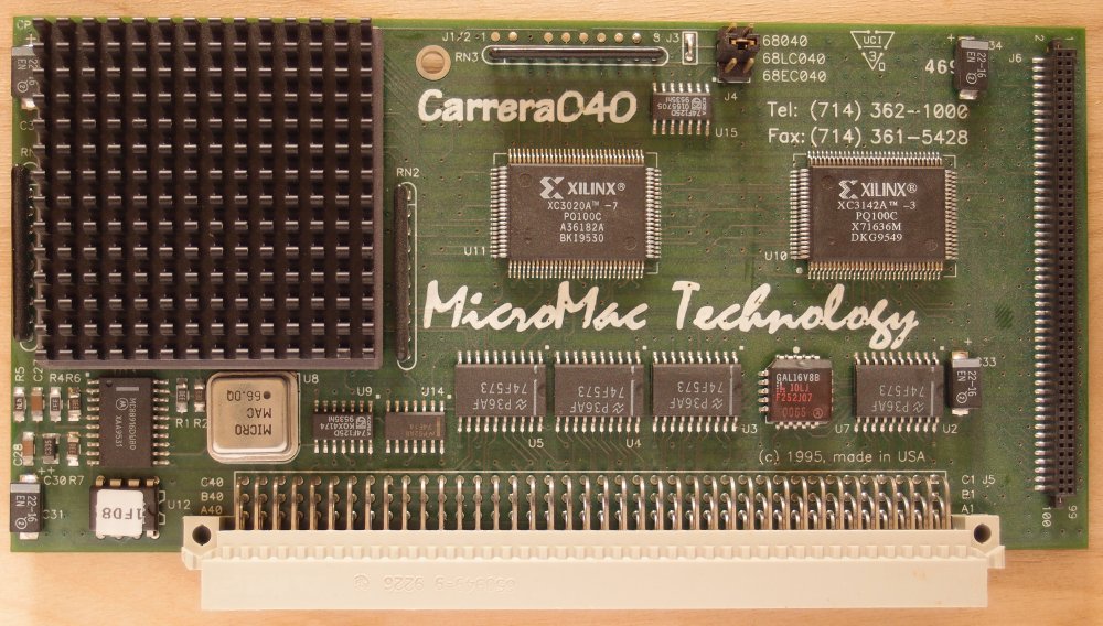
The MicroMac Carrera040

For many years I had a Carrera040 (or C040 for short)  – a Motorola 68040 accelerator for Apple Macintoshes – in my locker which I bought in wise foresight without even owning a Mac to plug it in. The C040 I got was meant for usage in a Macintosh IIci, plugged into its L2 cache-slot. That said, using special adapters, the C040 could also be used in other 68030 Macs like the IIx, IIcx, IIsi, IIvi/vx and the LC/LC II.

Is the Carrera a Speedster?

What’s this question about? Well, you might also have come about notions of an accelerator called the ‘Mobius Speedster‘ which is pretty similar to the C040.
Well, it is and my wild assumption is that at one point MicroMac bought the design from Mobius. There’s even a leftover in the C040’s ReadMe:
Applications that do not work with Quadra or Centris Macs are not likely to work on ‘040 accelerators, including the Carrera040. Generally, these incompatibilities are limited to the ‘040’s copy-back cache, or FAST mode on the Speedster.

So when I had my glorious SE/30 sitting on my desk it immediately came to my mind to make this card running in it.
You have to know, that the SE/30 is a somewhat shrinked-down version of a Mac IIx which again is pretty close to the IIci – and there was an adapter in existence to use another popular IIci accelerator in an SE/30 (Daystar Turbo 040). But it’s very rare and there’s next to no chance to find one. Anyhow, it’s doable, so I was hooked.
I stumbled across a cry for help in the 68kmla forum, a user owning such an adapter and a C040 tried to get it running in his SE/30… to no avail. So while still not having the proper adapter (yet) I thought “why not start looking into the driver while waiting for the hardware?”.
So the journey started…

MacNosy – a users nightmare, a hackers heaven.

My natural reflex is to reach deep into my tool-bag, get out my favorite disassembler/hex-viewer and start digging through its output. But for System 7 my bag was empty. Is there any disassembler at all?
While the good thing is, that most software packages which cost plenty of $$$ back then are abandonware today, the bad thing is that many are undocumented and unsupported. After some research it became clear that MacNosy was and still is the best m68k MacOS disassembler around.

Boy, this disassembler is powerful! But it seems to be written by Steve Jasic for, well, Steve Jasic. I know that kind of tools – I’ve written some of those… and never showed it to anybody because it was, erm, special. Prepare yourself for “everything will be different than you’ll expect it”. Steve gave a sh!# about UI or keyboard conventions. Cope with it.

Luckily there’s a very good review and some sort of documentation can be found here.

Same but different – which is where?

Does ‘A5-world’ ring a bell to you? No? Don’t worry, it was the same for me, even I am using Macs for a long time.
Even it’s an 68k system, there are so many things done different than e.g. in Amiga OS or Ataris TOS – so you have to learn a lot.

Because it would absolutely bloat this post, I will link to external pages explaining the used term. So watch for the first mentioning, it’ll be a URL…

The provided Carrera040 “drivers” consist of an INIT/Extension (“Startup Carrera”) and a Control Panel (“Carrera 040 1.8”).
In the provided readme file there’s the line “With version 1.8 we have included an extension which ensures the Carrera040 code to load very early in the boot process.

And indeed, the INIT code does not do much more than loading a specific resource from the control panels resource-fork.
So I concentrated on the control panel (CP for short). Using ResEdit, you’ll find the main detection and control-code in its resource fork called “SPDR’ (SPeedster DRiver, got it?).
While working through the code, commenting whatever I immediately understood (which wasn’t much in the beginning), I stumbled over several things you should also have an idea about before reading the disassembly in the coming chapters – so here’s a growing reading list:

Macsbug reloaded

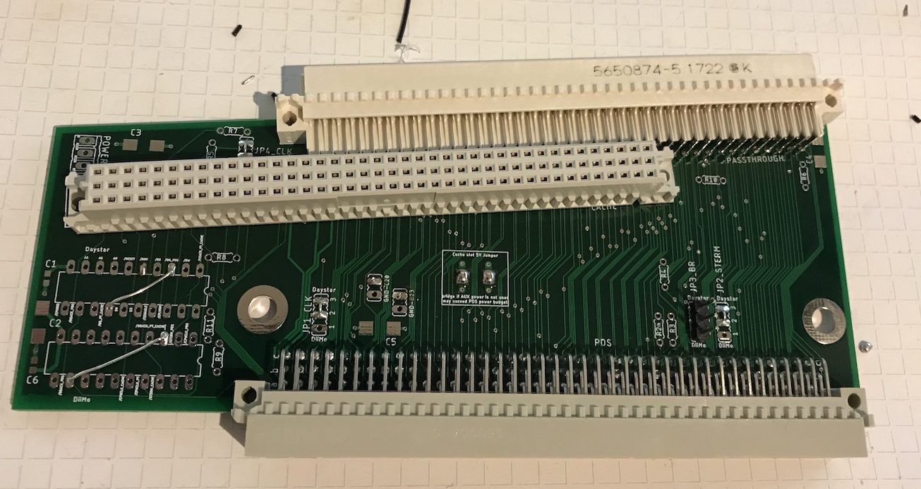
During all that code-gazing, head-scratching and learning-new-things-every-day great luck struck and I virtually-met ‘Bolle‘. A guy who created a clone of the mystical PDS-to-IIci-slot-adapter. Woohoo!

Even those 120pin DIN connectors are incredibly hard to find.

So after spending some Euros I was finally able to  jump into the ‘the real thing’ and try my patches in-vivo, or watch the code being executed. Thanks again, Bolle!

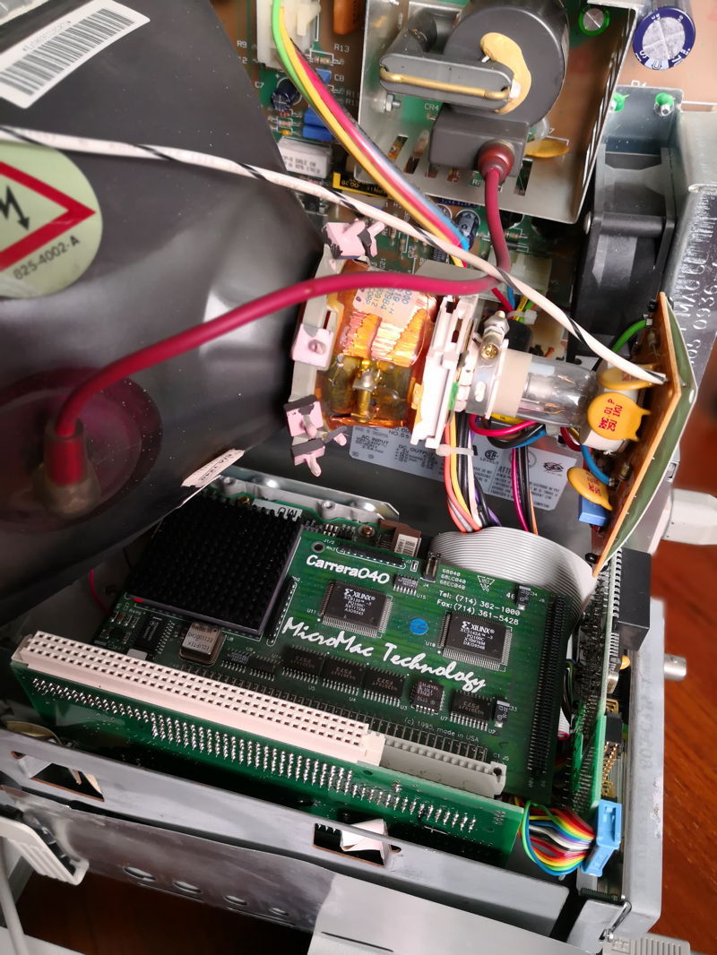
My C040 cramped into my beloved SE/30

The drill

The weapon-of-choice for watching code run is definitely Macsbug, the official debugger from Motorola, heavily modified by Apple through all the years until MacOS 9.2.
Back in the days my contact with Macsbug was very brief. When a program ‘bombed’, I’ve entered “g” (for Go) and hoped the system will somewhat heal and keeps running…

Ok, now I had to be somewhat more serious – and my skills had improved over the last 20 years, so my routine turned into single-stepping and tracing through the code, skip certain instructions which might kill the code, watching all the registers and most important and watch how the Carrera “driver” behaves in an SE/30 vs. IIci.
I even created some macros (which have to saved into Macsbug own resource-fork!) and started an endless try-and-crash drill.

The working drill is tedious: You step through the instructions, while following your steps in the disassembled source, to the point where it crashes. Remember/note the point (address) where it crashed and try again.
This means you have to manually trace closer to “the edge” but try not to fall off the cliff. And when you did – and I did many times – rinse & repeat.
Sometimes you can ‘skip’ complete function calls containing hundreds of instructions (called ‘Trace’), sometimes you have to sit-through (i.e. single-step) a very, very, very long loop just to be sure it works 100%.

The next post/chapters will finally dive into the control panels code.
While it’s all about this specific ‘driver’ I’m sure it’ll help everybody who starts the adventure of understanding pretty low-level 68k Macintosh code.

That said, in Dec. 2019, continuously working with Bolle, we came to the conclusion it has to be a hardware problem and Bolle was able to prove this and most importantly found a way to fix it.
There will be a 4th and final post concluding all of our findings.


Frankenpal

This is a hack which is very similar to the DesperRAM. It was born out of pure despair, so it’s neither elegant nor very clever – but it works and that’s what counts.

During the “BOZO resurrection“, I had one specific PAL under suspicion to not working correctly any more. That PAL was soldered (i.e. not socketed) onto the board in a very tight spot, so I wasn’t able to cut the pins as close as possible down on the board.
I know, there are special pliers which can somewhat around corners, but my trustworthy Knipex (The pliers maker in the world, full stop.) can’t. So I had to cut the pins right at the PALs package – easy and quick.

The downside is that this method leaves you with a leg-less IC… and if you then decide it might be useful to read-out that IC (like I did) it’s time to slap your forehead :-/
But not so fast, young Padawan. Despair has the advantage that it normally can’t get worse, so nothing to lose. Even you cut the legs off you still can spot the tiny remains leading into the package. So why not trying to replace the amputated legs with artificial limbs!?

My initial thought was soldering new pins to the package, but the remaining connection is way too small to allow anything to be soldered to it but a human hair.
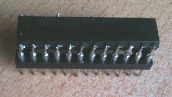
So I used a socket, turned upside-down, slightly bent the legs inward, squeezed the PAL between the sockets legs and carefully soldered the pins to the case-connectors. Finally I put small bits of wire into the sockets empty holes to create new pins to connect the whole thing to my GAL-programmer. Voilá: FrankenPAL

FrankenPAL

Yes, it looks horrible and I was quite sure that this doesn’t work but it just costed me 10 minutes, so what the heck, let’s try read-out that beast.

What should I say? It worked right on the first try… So never despair as long as you have a working solder iron 😉

Dissection time!

Ok, as I’m probably the last person on this planet fiddling around with the NumberSmasher i860, it was either “help yourself” or bust.

Given the fact that there’s an INMOS C012 on the card I tried my luck with the standard address of 0x150 and checked it with DOS’ crappy old ‘debug’. To my surprise I was able to talk to the C012, so it was very worth to investigate further.
So out went the good ol’ EPROM programmer and the EPROM of the card was dumped into a file.
I have 3 of those boards, two having a label on the EPROM saying “v1.1” and “BOOT_B2”. Both are identical… if you happen to own a NumberSmasher with a different label, get the dumpfile here for comparison.

That was easy, now the harder part: Disassembly. I had to revive my i860 machine language skills again, so it took me 2 days (on and off) to get a full understanding, what’s happening in there.
For those i860 assembly geeks among you, here‘s the fully commented code.

This “BIOS” is actually pretty simple. It’s just what I’d call a “PeekPokeStarter”. The main loop is waiting for a ‘command’ coming in by the way of the C012. This command can be either “0” or “1” as mentioned in the article on the previous page.

“0” means POKE (ie. write) and expects 4 bytes for the address and 4 bytes of data to be written (Both LSB first, Intel-style). So the full command reads: 0 00 00 00 20 78 56 34 12 or “write to address 0x20000000 the value 0x12345678”

So in consequence “1” means PEEK (ie. read) which just needs 4 bytes for the address to be read. The command would then be 1 00 00 00 20 or “read from 0x20000000”. The “BIOS” will then put 4 bytes to the C012 port at 0x150, which requires 4 reads from the PC side getting “78”, “56”, “34” and “12”.

Pretty simple, huh? But how can I start a program after it’s been painstakingly poked into the NumberSmashers RAM? Here’s the trick:

Poking to address 0x00000000 means start from the address given as data. E.g. “write to address 0x00000000 the value 0x20000000” is actually “start from 0x20000000”, or as command-chain: 0 00 00 00 00 00 00 00 20 – so beware of poking to 0!
Also, starting a program seems to disable the EPROM, so communication to the C012 is cut off if the running program isn’t handling this itself.

That’s about it. Nothing more in the “BIOS”… that’s why only 495 bytes(!) of the 8K EPROM are actually used. This simplicity leads to a very simple memory-map:

Base =  0xF8000000
C012-InData = [base] + 0x07
C012-OutData = [base] + 0x0F
C012-InStatus = [base] + 0x17
C012-OutStatus = [base] + 0x1F

Next task: Get a program running on the NumberSmasher.

[11/11/10] Great News…again! It was easier than expected… the first program running on the NumberSmasher-860! So read on in the next post…

Hacking the AVM T1

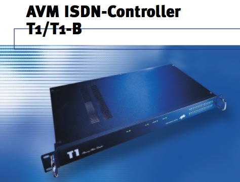
AVMT1Press

It was inevitable… the biggest system AVM built was the “T1”, a 30 channel ISDN controller in a sleek 1U 19 inch case of which nothing more than the above marketing picture seems to exist.
One fine day I had to had one – and today is the day!

I was able to find a AVM T1 on ePay which was not very well advertised so I had no “professional competition”. Even I didn’t spent a fortune it was a bit of gambling because I didn’t knew what to expect.
Besides AVMs own T1 PDF manual there’s next to nothing available in the Web – So this section is yet another WWW-exclusive brought to you by geekdot.com 😉 (Ok since 2009 others discovered this page and also this cheap entry into the wonderful world of multi Transputing)
Still, the docs said “a Transputer network with 9MB RAM” so I couldn’t go completely wrong. That said, I was expecting SMD T400s at AVMs usual sluggish speed…

First look

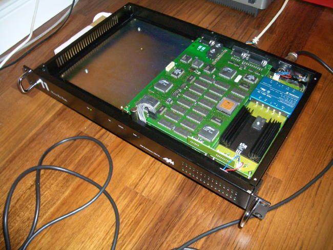
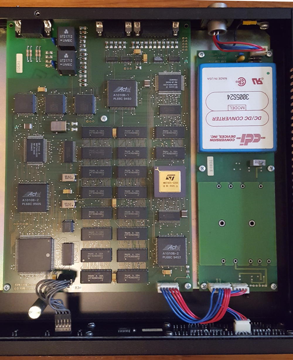
When the box arrived first thing was getting out good ol’ screwdriver and open the case…

AVMT1open

…and I was very surprised:

  1. A socketed T425 – so that’s another easy upgrade then.
  2. An external power supply (48V)! That’s strange but also neat – no noise and next to no heat in the case itself
  3. Also, the board is very small…  lot’s of room left in the case.

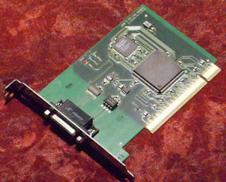
That’s done by intention as you could buy the T1-B, where “B” stands for the “Booster Board”, yet another board with 4 more Transputers and another 8MB of RAM giving a total of 7 Transputers and 17 Megs of memory. Quite a setup for just an ISDN controller.

Sniffing around

Ok, this beast has to do something better than handling 30 boring B-Channels… Mandelbrot for example 😉 So let’s see how this thing is/was supposed to speak to the outside world.

The manual is talking about an ISA or PCI controller-card which will be connected to a 9-pin Sub-D connector. Having a closer look to the mainboard where that connector is seated I discovered some other old friends: AM26C31 and AM26C32.
Aaaaalrighty, RS422 time… that’s the same way my Tower of Power is transmitting its data. So I can use my TTL-to-RS422-converter I’ve built for the Gerlach card.

Out goes the multimeter and after a while I figured out the the traces on the board. For a better understanding, here’s the “map”:

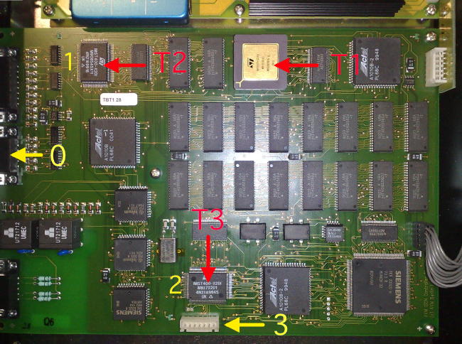
AVMT1Board

Marked by the red arrows are the three Transputers:  T1, a T425-25, is the “application processor” while T2 and T3 are more simple T400-20 handling the ISDN subsystem.

The yellow arrows mark the four links of the T425 – which is probably the reason why AVM used a 425 vs. their usual T400: this time they really needed 4 links.
Link0 is connected to the 9-pin sub-D connector (via the RS-422 transmitters/receiver) for interfacing to the PC.
Link1 and Link2 are directly connected to the T400s.
Link3 goes to the connector on the lower edge of the board. I bet this is where the “booster board” would be connected… not a hard bet, I admit.

The pinout for the 9-pin sub-D connector (female) is:

 1 Link0-IN -
 2 N/C
 3 Reset-IN +
 4 N/C
 5 Link0-OUT +
 6 Link0-IN +
 7 Reset-IN -
 8 GND
 9 Link0-OUT -

As Link0-IN and Reset-IN are routed through two separate 26c32 I assume there might be more differential signals available. If time allows I’ll dig deeper on this matter.

Do something Gromit!

Well then… a cable was built in a couple of minutes – some cursing and swearing about the differential polarity and then the exciting moment came: Let’s see if it’s really so easy again!

It is! And here’s the ispy output for the T1 (connected to the “Gerlach card”):

Using 150 ispy 3.23 | mtest 3.22
# Part rate Link# [  Link0  Link1  Link2  Link3 ] RAM,cycle
0 T800d-25 288k 0 [   HOST    …    …    1:0 ] 4K,1 1024K,3;
1 T425c-20 1.6M 0 [    0:3    2:0    3:0    … ] 4K,1 4092K,3.
2 T400c-20 1.7M 0 [    1:1    …    …    … ] 2K,1 1022K,3.
3 T400c-20 1.8M 0 [    1:2    …    …    … ] 2K,1 4094K,3.

Some remarks about this:

  • 9 MB is true. The “application processor” (T1) got 4MB while the two T400s got 1 (T2) and 4 MB (T3, obviously connected to the SIEMENS Munich32 Über-ISDN controller).
  • While the built-in T425 is spec’ed for 25Mhz it’s just running at 20MHz… what a waste of bang… and what an opportunity for improvement :->
  • The linkspeed is at maximum… which one would expect with directly connected links. But with AVM you’ll never know 😉
  • The RAM-speed is pretty good (compared to what they did to the B1) – even they just used 70ns RAM.

Next up: Having fun with Mandelbrot! Having just T4xx Transputers it can only use the integer algorithms (i.e. no floating point) but who cares for a quick start?!

It’s working and showed another nice gadget: LEDs! Each Transputer has a tiny SMD-LED connected to it’s Link-Out.
So having the T1 underneath the table I have quite a nice light-show while the three are working their a** off 😉

If you happen to have no access to a RS422 converter: Never say die!
Like said above, there’s still Link3 available – normally meant for the booster-board – and it’s pure TTL. All you need is a somewhat non-standard plug to this connector. Be creative but don’t forget that unbuffered link connections only allow a distance of a couple of inches/centimeters!

The pin-out (so far) is, counting from left to right:

 1 - 5V VCC
 2 - T1 Link3 OUT
 3 - T1 Link3 IN
 4 - RESET
 5 - T3 Link1 OUT
 6 - T3 Link1 IN
 7 - GND

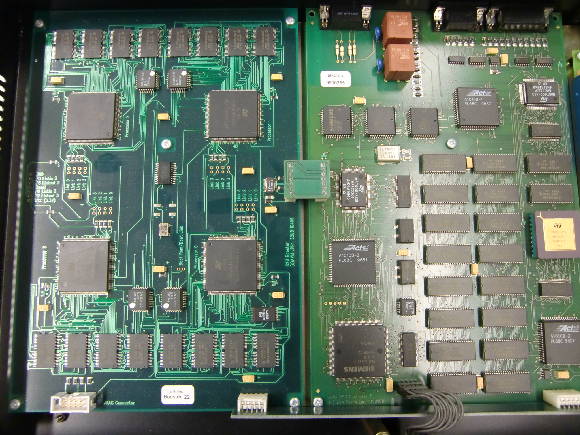
[UPDATE 11/14/10] Again, with some ePay-Luck I got another T1… and it again was some kind of lottery… and I had luck! This time it’s a T1-B!! This means, the “booster board” is installed. So opening the case, it looks like this. On the right the normal T1-board, to the left, “da mighty booster board” 😉 I’ll call it “BB” from here…T1-Booster-Full

As expected, it’s connected via Link-3 of the T1 Board. On the lower edge of the picture you can spot the power-supply “module”. It’s longer than in the T1 configuration and provides 3.3V/GND to the BB, i.e. the BB is 3.3v only!!

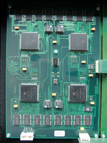
Here’s the BB alone:

T1-Booster-Board

All in all the BB is more modern than the T1-board. Very suspicious are the JTAG connector on the lower left having its lines connected to a EEPROM (AT28V256, right edge of the BB board, above the row of RAMs). Further up, left to the CPU nearby is a pad with the lable “Boot from ROM/Link”. I wonder what the default is and what’s inside that EEPROM – will investigate later.

Most importantly the BB board features 4 ST20450 processors, which aren’t INMOS products anymore. They were designed by ST after they bought INMOS. For short, the ST20450 is a T425 on steroids. More on-chip RAM (16K), higher clocking (40MHz) and some more instructions.
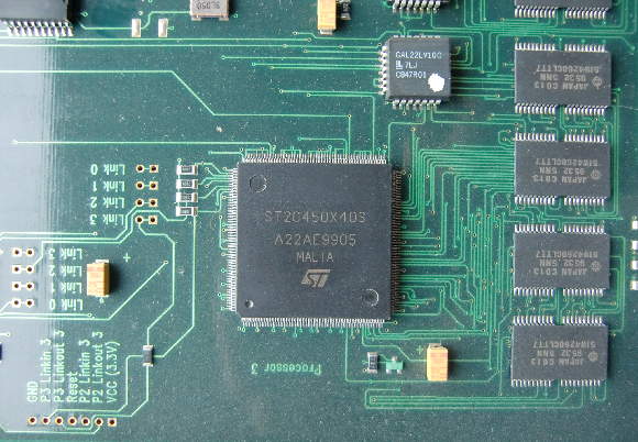
Each ST20450 has its own 2MB of RAM and a GAL handling the memory etc.. Here’s a close-up of a single ST20450 “module”:

T1-Booster-1of4

Mind the careful markings/labels on the board. The CPUs are numbered (“Processor 3”) and there are pads for Links etc.

Finally, I currently have no tools to check/use ST20450 processors. ispy finds the Transputers on the T1 board but freaks-out when it pings the ST20s.

Here’s another new addition: A picture of the official T1-PCI interface. It contains a PCI-controller (the big IC) and a XILINX FPGA… probably containing a synthesized C011.

T1_Interface

UPDATE:

Jonathan Schilling also plays played around with an AVM T1 on his page including the original ISA controller card… and he‘s making made very good progress!
[2015, Jonathan quit ‘the scene’ and handed over all his equipment… further on, it seems in 2020 he closed his pages]

Another UPDATE [2017]:

Just got another T1 off ePay… surprisingly it contained yet another board-design. I’ll call it the “non-booster layout“. This board has no connectors for the booster-board and missing the regulator below the DC/DC converter – no need for 3.3V.

TODO: 

  • Change the T425
  • Make the 30 front-panel LEDs blink
  • Figure out for what the female 15pin sub-d connector is good for (not mentioned in the manual)

Here’s how to access the LEDs at the front – thanks to Michael Brüstles research:

typedef unsigned long int u32;

/*
 *  addr XXXX-XXXX-X111-XXXX-XXXX-XXXX-XXXA-AA00
 *    
 *  wr                               0-01    __ EN __ __-__ __ __ SY
 *  wr                               0-10    08 07 06 05-04 03 02 01
 *  wr                               0-11    16 15 14 13-12 11 10 09
 *  wr                               1-00    24 23 22 21-20 19 18 17
 *  wr                               1-01    SC ST 30 29-28 27 26 25
 *
 *  rd                               0-01    readable ... content unknown
 */

int main( void ) {

    u32 *p = (u32*)0x80700000UL;

    p[ 1 ] = 0x40;  /* enable all leds 0x40 & Sync 0x01 */
    p[ 2 ] = 0x05;  /* Led01-Led08 */
    p[ 3 ] = 0x00;  /* Led09-Led16 */
    p[ 4 ] = 0x3F;  /* Led17-Led24 */
    p[ 5 ] = 0x92;  /* Led25-Led30, System, S-channel */

    return 0;
}

Fixing scratched traces

This is the price you have to pay if you’re into real men’s hardware:

Being (falsely) identified as “old crap”, some cool things end up in the dumpsters… or worse. Being tossed around in some storage for years, probably stacked with other cards and boards, it might happen that some traces on the outer layers got badly scratched, thus making the board/card non-working. Here’s how I try to fix scartched traces… and most of the times it works:

First make sure that the circuit path (trace) is really broken – I just may look like, but isn’t.
To do this you need a volt-meter. Follow the suspected trace in both directions until you find a pin or through-hole it is connected to. Use these two points to test if the trace is still connected.

Ok, damn, it’s broken 🙁 You need three things:

  1. A sharp knife or scalpel
  2. Adhesive tape (Scotch, Tesa or whatever it’s called in your corner of the world)
  3. Conductive (silver) lacquer

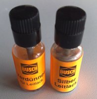
Conductive-what? Conductive lacquer is actually a cool thing to play with… but be prepared: It’s not cheap (about 9-10 Euros). It comes in tiny bottles or as a pen, which is even more expensive (20+ Euros). The bottles look like this (lacquer and diluter):

ConductiveLacquer

Ok, the process is quite simple:

  1. Use the knife to scratch-off some of the coating lacquer on both ends where the trace was “cut” until you see some copper shining through.
  2. Check with your volt-meter that you actually have contact with one end and e.g. a pin on the other end of the trace. Do this for both “halves” of the cut trace.
  3. Mask the place you’re going to ‘heal’ with your adhesive tape – this prevents the conductive lacquer to run all over your board.
  4. Apply the conductive silver lacquer onto the spot you’ve just masked and let it dry (read the manual that came with the lacquer – yeah it’s unmanly but nobody will see you ;-))
  5. Using your volt-meter, check again. This time from both ends of the complete trace.

If you’ve done everything right, the  trace should work again – and so does your card/board! Yay!

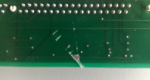
Here’s how my badly scatched MiroHIGHRISC looks like in certain places – can you spot the little silver dot?

FixedPath

Final hit: Some lacquers are quite thin on silver (blame the manufacturer) so after some days the spot you just fixed might become unreliable. In this case you might repeat the procedure to get more silver to that spot.

Removing pin rows

Removing pin rows…doh! It took me quite some time to figure out a working solution for this problem, so I thought it might be useful to you some day, too.

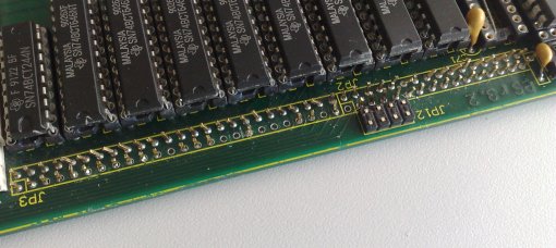
Some idio^h^h^h^h not so clever person cut off all the pins on one of my DSM860 RAM boards – I probably will never figure out why (may a lightning hit him!). Besides 8 of the pins all other 74 (!) where cut, rendering the ram card non-functional (it’s the memory bus connector).

Here’s a (blurry enlarged) picture of the mess:

DSM860-RAMcard-Pins1

I started to desolder some pins from the back-side of the card but soon found out that the solder was too old to be removed the classic way (desolder pump & wick). Also, that pin-row (41×2) was one piece, so I would have to completely remove all the solder before I would be able to pull the part from the card.

After some thinking I came to this solution, which worked quite good:

First you need to cut away the plastic part from the top of the board. I used a very fine and sharp  caliper to cut away one pin after the other (i.e. like a single jumper).
While doing so be careful not to cut into the board!
Then pull or push the plastic pieces from the pins, again one after the other – I used a thin knife pushed under the plastic an gently wiggling it over the pin.

When done, it should look like this:

DSM860-RAMcard-Pins2

You may spot that some pins are missing already – that’s because my previous desolder tries sometimes seemed to work. Still, I couldn’t avoid that some pins got bent. This is the time for my secret repair tools: Syringe needles!

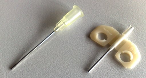
Second, get two kind of needles:  Gauge 18 and 20, that is 0.9mm and 1.2mm, color code yellow and pink. Cut off the tip of the needles and use a rasp to make the edge straight and clean. They should look like this then:

Needles

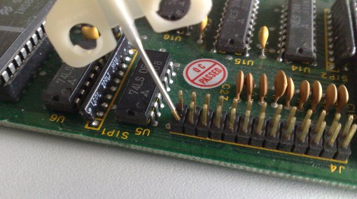
The bigger needle (G20) is just perfect to be completely pushed over a pin which then can be bent into any position without the risk of breaking it off – it works like this:

BendPins
(This is just a showcase picture with a different board, the needle needs to be pushed all the way down over the pin)

So straighten all the pins into an upright position. This will be important for the next step!

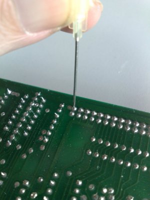
Now put your board into a vertical position (e.g. fixed by a bench vise or clamped between your inner thighs ;-)), get out your solder iron and the G18 needle – this needle should be just small enough to fit through a pin-hole.

This is the third and last step. Place the G18 needle over the pin you like to desolder on the back-side of the board like showed here:

PushPins

From the other side you’re touching the base of the pin with your solder iron. As soon as the solder starts to melt gently push the needle onto the pin.
If everything works like it did for me, you will push the needle through the board, including the solder and the pin you’ve planned to remove!

The great thing with this is that the needle (being made of steel) does not stick to the solder. As soon as the needle got a bit colder, you can easily remove the pin as well as the excess solder from the needle with your fingers!
Now carefully pull back the needle through the board and you should have a nice and clean through-hole in the board. If not, a final cleaning with a desolder-pump or wick should do it.

This needle-trick also works brilliantly with empty pin-holes which got filled with solder. Just place the needle on the pin-hole on one side of the board, heat up the solder on the other side while pushing the needle. Pop! There goes the solder!

As said, this technique worked great for me. All 82 pins got removed, a new pin-row was soldered into place and the card is now working like a charm.

Still, do this at your own risk!
I’m not going to be taken liable for any damage to your board or your health!
If your unsure if you are able to perform this stunt, don’t do it!
Practice with an old scrap board/card before you fiddle with the “real thing”!