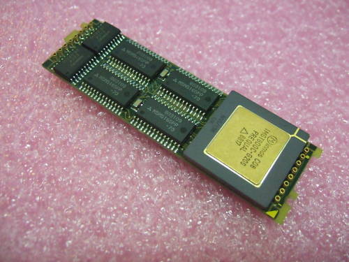
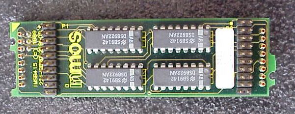
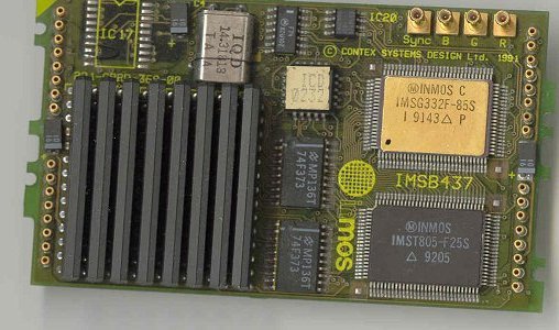
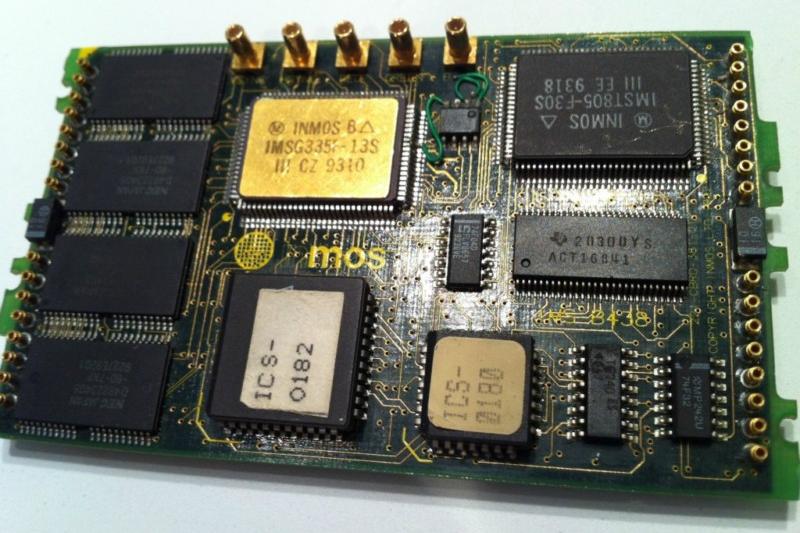
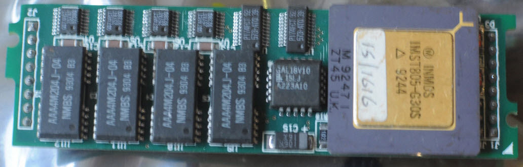
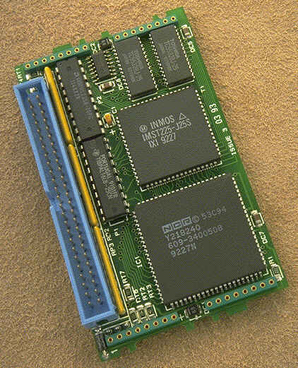
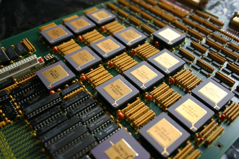
Category Archives: Knowledge Base

Removing pin rows

Removing pin rows…doh! It took me quite some time to figure out a working solution for this problem, so I thought it might be useful to you some day, too.

Some idio^h^h^h^h not so clever person cut off all the pins on one of my DSM860 RAM boards – I probably will never figure out why (may a lightning hit him!). Besides 8 of the pins all other 74 (!) where cut, rendering the ram card non-functional (it’s the memory bus connector).

Here’s a (blurry enlarged) picture of the mess:

DSM860-RAMcard-Pins1

I started to desolder some pins from the back-side of the card but soon found out that the solder was too old to be removed the classic way (desolder pump & wick). Also, that pin-row (41×2) was one piece, so I would have to completely remove all the solder before I would be able to pull the part from the card.

After some thinking I came to this solution, which worked quite good:

First you need to cut away the plastic part from the top of the board. I used a very fine and sharp  caliper to cut away one pin after the other (i.e. like a single jumper).
While doing so be careful not to cut into the board!
Then pull or push the plastic pieces from the pins, again one after the other – I used a thin knife pushed under the plastic an gently wiggling it over the pin.

When done, it should look like this:

DSM860-RAMcard-Pins2

You may spot that some pins are missing already – that’s because my previous desolder tries sometimes seemed to work. Still, I couldn’t avoid that some pins got bent. This is the time for my secret repair tools: Syringe needles!

Second, get two kind of needles:  Gauge 18 and 20, that is 0.9mm and 1.2mm, color code yellow and pink. Cut off the tip of the needles and use a rasp to make the edge straight and clean. They should look like this then:

Needles

The bigger needle (G20) is just perfect to be completely pushed over a pin which then can be bent into any position without the risk of breaking it off – it works like this:

BendPins
(This is just a showcase picture with a different board, the needle needs to be pushed all the way down over the pin)

So straighten all the pins into an upright position. This will be important for the next step!

Now put your board into a vertical position (e.g. fixed by a bench vise or clamped between your inner thighs ;-)), get out your solder iron and the G18 needle – this needle should be just small enough to fit through a pin-hole.

This is the third and last step. Place the G18 needle over the pin you like to desolder on the back-side of the board like showed here:

PushPins

From the other side you’re touching the base of the pin with your solder iron. As soon as the solder starts to melt gently push the needle onto the pin.
If everything works like it did for me, you will push the needle through the board, including the solder and the pin you’ve planned to remove!

The great thing with this is that the needle (being made of steel) does not stick to the solder. As soon as the needle got a bit colder, you can easily remove the pin as well as the excess solder from the needle with your fingers!
Now carefully pull back the needle through the board and you should have a nice and clean through-hole in the board. If not, a final cleaning with a desolder-pump or wick should do it.

This needle-trick also works brilliantly with empty pin-holes which got filled with solder. Just place the needle on the pin-hole on one side of the board, heat up the solder on the other side while pushing the needle. Pop! There goes the solder!

As said, this technique worked great for me. All 82 pins got removed, a new pin-row was soldered into place and the card is now working like a charm.

Still, do this at your own risk!
I’m not going to be taken liable for any damage to your board or your health!
If your unsure if you are able to perform this stunt, don’t do it!
Practice with an old scrap board/card before you fiddle with the “real thing”!

The EISA Bus

Actually I have no idea why this subject caught my interest so well.
During the hey-days of the EISA bus I wasn’t interested at all, thought that’s something which will never take off and was intended for servers only. I happily stuck to clumsy ISA and sat there until PCI was affordable (ASUS SP3G anyone?).

Now, fiddling with all those exotic cool mainboards, EISA crosses my path all the time. The way EISA is configured, the somewhat cumbersome use of cf.exe (ECU – EISA Configuration Utility) tool drew my interest… maybe because it has the scent of manliness 😉

In my humble opinion, EISA was a crutch, but it layed some basics for the next 10 years:

  • It defined (as a by-product) a standard for the ISA bus, which was all chaotic before
  • It forced Big-Blue (IBM) to think over their Microchannel licensing
  • It was a test-bed for how do things right… later known as PCI

That said, it is the fun twilight-zone between ISA’s direct access “do what you like” and PCI’s “you touch – you die” approach. Where else do you have 32-bit speed and can still change bits manually with DOS’ debug?

Intel EISA Chipset

This chipset started it all… it was the first EISA chipset produced and the one which riddled me the most. Mainly because I have two EISA boards behaving differently when it comes to expansion cards which were developed later (~1992-94) and so I suspected the Bus Controller to be the reason for all the hassle:

The Hauppauge 4860, an early EISA system and my Intel Professional Workstation (aka LP486, not yet documented on this page).
The first is using a 82350 chipset while the latter has a 82350DT. Where’s the difference? There’s no clear answer to this anywhere, so I had to do some lenghty, in-depth research.
Good that I do not only collect ancient cool hardware but also some documentation, e.g. the 2″ thick Intel “Peripheral Components” handbook from 1991…

Intel_Periph

Here’s my conclusion:

The ‘original’ 82350 Chipset -released May 1990- included just 2-3 chips: 82357, 82358(-33) and (optionally) 82352.
The 82350DT -released April 1991- consisted on 5-7 chips: 82357, 82358DT, 82359, 82351, 82352, 82353 (some of them used multiple times).
The difference between the non-DT and DT version of the 82358 seems to be the synchronous interface to the 82359 DRAM controller, which wasn’t available in the initial chipset.

Chip-by-chip round-up of the chipset:

The 82350DT EISA chip set contains 7 VLSI chips to build a complete EISA
system. It is built upon the 82350 EISA chip set utilizing the 82358DT EBC and
82357 ISP and then adds VLSI components:

  • 82359 DRAM controller.
  • 82353 Advanced Data Path,
  • and 82351 LIOE Local IO Peripheral

The picture below shows a 486 based system with 82350DT chip set.

illu

The host bus connects the CPU and the memory subsystem. Tlte peripheral bus (X-bus) is an 8-bit bus to support the motherboard IO functions: keyboard, floppy and the LIOE which integrates the parallel port; and support: extemal teal time clock und serial ports. The peripheral bus is a buffered version of the 8-bit ISA bus. The memory subsection operates independent of the CPU clock. This independence is accomplished through the use of 82359’s integrated programmable delay line and the  rogrammable state tracker(PST) function. The integrated programmable delay line is used to time precisely the DRAM cycle sequence to DRAM parameters. The PST resides cm the CPU module. Tite 82359/82353 reside on the motherboard. They are indifferent to the CPU/cache used. The PST converts processor cycles to a form acceptable to the 81359. This allows different CPU/ cache combinations to be connected to the same motherboard. Further, it translates CPU’s clock-dependent handshake to clock-less memory interface handshake.

Local I/O EISA Support Peripheral, lntel 82351

The 82351 supports or integrates all of the IO peripheral functions for a typical EISA system board with a minimum of external logic. lt integrates local I/O ddress decoder, EISA system configuration registers, two external serial I/O ontroller interfaces with four assignable interrupts generation, external EISA onfiguration RAM interface, parallel port interface, external floppy disk controller Interface, external keyboard (8×42) controller interface including interrupt generation, and external real time clock interface and EPROM or FLASH EPROM BIOS ROM interface. lt was available in a 132-pin PQFP (Plastic Quad Flat Pack) package.

EISA Bus Buffer (EBB), Intel 82352

The 82352 is a bus buffer IC for EISA bus system. Three 82352 chips are used in a 82350 EISA system. Only one 82352 chip is used in a 82350DT EISA system.
lt operates in three modes. ln Mode 0 it performs data latch and swap functions.
It allows swapping and assembly of  data between the host and EISA/ISA buses on a byte by byte basis. In Mode 1 it provides 1 buffered path between the host data bus and DRAM with parity generation/check. Mode 2 was reserved by Intel for future use (never happened). Mode 3 provides address latching function between the host and EISA/ISA buses. The 82352 was available in 120-pin quad flat pack (QFP).

Advanced Data Path, Intel 82353

The 82353 provides advanced data path in e 82350DT EISA bus system. Two 82353 chips are used in a 82350DT EISA bus system as showed in the graph. Each 82353 is designed as a 16-bit slice. Two 82353 chips can provide parallel interface to 32, 64 or 128- bit wide memory structures to a 32-bit host and system bus.
The 82353 provides optimal 486 burst performance. Each memory cycle enerated by the address controller chip causes 128 bits of memory data to be latched in two 82353 chips. Once data is latched, these 82353 chips mux the four dwords to the destination in one wait state. The 82350DT EISA bus has 128-bit memory bus. A typical burst is 128-bit wide. and a bus with the same width
allows to read the whole burst in one memory cycle. This provides a zero wait state burst at any frequency. The 82353 was available in a 164-pin PQFP package.

Integrated System Peripheral (ISP), Intel 82357

The 82357 contains DMA controllers, interrupt controllers and programmable 16-bit counter/timers. lt provides high-performance arbitration for CPU, EISA/ISA bus masters, DMA channels and refresh. It also provides logic for generation/control non-maskable interrupts. The DMA function is provided by two inbuit 82C37A DMA controllers. These DMA controllers are connected in cascade mode to provide seven independent programmable channels. The timing control for 8-, 16- and 32-bit DMA data transfer is provided. The data transfer rate is 33MB/sec. There are two 82C59A interrupt controllers in the 82357 chip, which provide 14 independent programmable channels for level or edge-triggered interrupts. The 82357 contains five 82C54 compatible programmable 16-bit timers/counters. lt was available in a 132-pin PQFP package.

EISA Bus Controller, Intel 82358DT

The 825358DT provides an interface between 386/486 CPU and EISA bus system.
It provides EISA/ISA bus cycle compatibility with the host(CPU) bus. The 82358DT is a part of intel 82350 and 82350DT chip set. It translates host(CPU) and 82359(DRAM controller) cycles to EISA/ISA bus cycles. lt supports 8-, 16- or 32-bit DMA cycles. lt also supports host and EISA/ISA refresh cycles. lt generates control signals for advanced data path(82353) and EISA bus buffer(82351). lt was available in a 132-pin PQFP package.

DRAM Controller, lntel 82359

The 82359 is a highly integrated advanced memory controller. lt supports 386 and 486 microprocessors. Its operation is independent of speed and type of the CPU. It allows a system designer to implement a variety of CPU/cache combinations. It provides address control, refresh generation and critical DRAM timing generation. In conjunction with two advanced data path devices (82353), it acts as a highly integrated 32-bit dual ported memory controller. Its two ports (or address gateways) to main memory are: one exclusively for the host and one exclusively for EISA. This configuration of ports permits CPU activity to be isolated from EISA bus activity. It controls up to 256MB of motherboard DRAM. It supports 32-, 64- or 128-bit wide memory configurations. lt was available in a 196-pin PQFP package.

Bus Master Interface Controller, Intel 82355

The 82355 is used in an EISA add-in card (expansion board) – thus rarely found on mainboards.
It supports 16- and 32-bit burst transfers at maximum data transfer rate of 33MB/s. It also supports 32-bit non-burst and mismatched data size transfers. It automatically handles misaligned double-word data transfer with no performance penalty. It has two independent data transfer channels with 24-byte FIFOs. Expansion board timing and EISA timing operate asynchronously. The 82355 supports 32-bit EISA addressability (4GB). It integrates three interfaces:
EISA, local CPU and transfer buffer. It supports automatic handling of complete EISA bus master protocol. This includes EISA arbitration/preemption, cycle timing and execution, byte alignment, etc. Further, the 82355 supports local data transfer protocol similar to traditional DMA. It was available in a 132-pin JEDEC PQFP package.

Inmos TRAMs

INMOS was obviously the first manufacturer of TRAMs. Over the time you can clearly see the progress the technology made over the period Inmos TRAMs were made. Starting with comparably big sizes, using DIP chips etc. the last of its breed were highly integrated PCBs cramped with SMD parts and chips.

The IMS B401 started it all. A 32KB SRAM size-1 TRAM for a 32-bit Transputer. Here’s the prototype, the final product and a picture of its schematic:

B401_Layout

The “huge” IMS B403 1Mbyte DRAM Size-4 TRAM:

IMSB403_1

The IMS B404 (2MB DRAM, Size-2) is where the fun starts. Size-2 is just OK not to totally hog your mainboard and 2MB is what you need for OCCAM or HELIOS to make something useful.
Actually, the B404 has 3 “levels” of RAM. 4K internally in the Transputer, 32K SRAM and 2048K DRAM. As they are superimposed (i.e. overlapping), the total amount is still 2MB with different access speed at 0-4k (1 cycle), 5-32k (3 cycles) and 4-5 cycles above.

IMSB404

There were also the IMSB402 (8Kbyte Size-1) and the IMSB405 8Mbyte Size-8 TRAMs of which I have no pictures yet.

The IMS B407 was an Ethernet TRAM (Size-8!), proving that a TRAM doesn’t need to be necessarily a Transputer Module for number crunching only.

imsb407

The IMS B408 and B409 were both part of a graphics system, so you didn’t the to have the host to render the graphics – which would have been much slower than those TRAMs.
The B408 was the “drawing pad image storage” (1,25MB dual-ported RAM), while the B409 had the timing generator and the CLUTs:

imsb408

imsb409

The IMS B411 can be seen as a new era: 1MB DRAM on just a size-1 TRAM made possible by the use of small ZIP-packaged DRAMs… which were very expensive, of course.

IMSB411-3B

The IMS B415 is a simple Transputer-Link to RS422 converter. This way, link connections can span up to 30 meters.

imsb415

The IMS B416 features a 16bit T2xx Transputer and 64KB SRAM

IMSB416_10P

The IMS B417 is a massive beast: 4MB on a size-4 TRAM… well, still better than the B403.

IMSB417-5A

The IMS B418 contains a 16-bit T222 and 256KB Flash ROM… quite modern stuff those days and probably a good way to boot your HELIOS system from 😉

IMSB418_1

The IMS B419 combined the two huge B408 and B409 modules into one size-6 TRAM. A nice graphics TRAM with 2MB DRAM and 2MB VRAM…

imsb419

The IMS B420 featured a ZORAN ZR34325 DSP (45 MFLOPS peak) with its own 256KB SRAM besides the obvious T800 Transputer and 4MB DRAM. My guess is, that it is comparable to the Quintek QVA-T TRAM.

imsb420_1

The IMS B421 enabled a Transputer system to talk to GPI/IEEE-488 buses … like laboratory equipment or your old Commodore Floppydrive 😉

IMSB421_1

Ahh, the real-deal… the IMS B426 is what you want in your TRAM collection. 4MB RAM on a size-1 TRAM. This is where Helios really loves to run on.

IMSB426-5A

…and here’s a more recent version of the B426 (rev “-16C”, 1993), this time all SMD, featuring the latest T800 in a nice TQFP case

IMS_B426

Well, the IMS B426 is great… as long as you can’t get the IMS B427 😉 This Size-2 TRAM features a whopping 8MB RAM. Enough for running Helios and X11 on it.

IMSB427

Something more important than ever is a fast network connection. The last ethernet TRAM from INMOS was the IMS B431.
10mbps is the maximum you get… well, more wouldn’t make sense given the Linkspeed of 20mbps.

IMSB431

The IMS B437 is a very neat little thing: A graphics TRAM as size-2 TRAM! A nice 25MHz SMD T805 and a G332 colo(u)r video controller. Rare as chicken teeth!
It looks like this was designed by Contex Systems Design Ltd. and OEM’ed by INMOS.

IMSB437_1

And when you thought you’ve seen them all, another one pops up:
The mighty IMS B438. As the name-code suggests, it’s an updated B437 – very updated and IMHO the ultimate graphics TRAM: 2MB VRAM, 4MB DRAM, 30MHz T805 and the last and final 32Bit video controller G335@130MHz. I really, really want one. Badly!

B438

Because it’s a beauty, here’s its back, too:

B438_back

HTRAMs

As the T9000 had so many new features and architectural differences the “classic” TRAM wasn’t enough to support all that. So INMOS went to enhance the TRAM-model…

And they meant it! Instead of DIL 16 Pins of a “classic” TRAM, HTRAMs could use up to 160(!) pins to communicate to the outside world. Besides the classic 5V, also 3.3V was supplied on one pin as a tribute to the technical progress. Due to the introduction of the DS-Links (vs. OS-Links within the T4xx familiy), each of the four links of the T9000 now required 4 pins per link, resulting in 16 pins for the links alone. Plus many other special links for Events, ConfigUp/Down etc. a minimum of 60 pins were used.
Also each HTRAM now featured a PROM so it could be identified by software.

This is the pinout of an HTRAM extracted from the most recent source (SGS-Thomson B92x HTRAM datasheet, Nov. ’94)

HTRAM

Pin Row a Row b Row c Row d Row g Row h
1
2
3
4
5
ClkIn
L0SIn
L0DIn
L0DOut
L0SOut
N/C
GND
N/C
V3V3
N/C
TDI
V5V0
CupSIn
GND
CUpDIn
notTRST
L2SOut
L2DOut
L2DIn
L2SIn
EventIn0
EventIn1
EventIn2
EventIn3
EventOut0
EventOut1
EventOut2
EventOut3
9
10
11
12
13
L1SIn
L1DIn
L1DOut
L1SOut
Reset
N/C
V5V0
N/C
GND
TMS
CUpDOut
GND
CUpSOut
V3V3
TCK
L3SOut
L3DOut
L3DIn
L3SIn
V5V0
1
2
3
4
5
N/C
N/C
N/C
N/C
N/C
TDO
GND
CDnSOut
V3V3
CDnDOut
9
10
11
12
13
N/C
N/C
N/C
N/C
N/C
CDnDIn
V5V0
CDnSIn
GND
N/C

While many (i.e. 100) pins left unspecified in this pinout-map (e.g. Block 2 rows c & d, Block 3 rows e & f and the complete Block 4), they’re all used on the HTRAMs I own.
My guess is that those were used for the memory-bus, at least in the case of my Quintek board.

Here’s an original INMOS HTRAM, with a 15MHz T9000 engineering sample mounted, plus a T9000 (backside) next to it:

HTRAMandT9k

For a quickstart here are the 3 HTRAMs from Quintek which I own:

QT9A

The QT9A (Rev.C in this case) is a processor HTRAM of (yet) unknown clock-speed and memory-size – I think it’s 4MB. Because the T9000 ran really hot in the prototype stage (which he never left), all of them required a compariby big heat-sink. I do not dare to remove it, given the (collector) value.

QT9A_front

…and the backside for completeness 😉

QT9A_back

QT9H

This is a display HTRAM featureing a Bt485 RAMDAC, 2MB VRAM but no video-output part. The video signal is delivered to a pin-row which is going connected to a VGA-featurebus on a graphics card. It’s a Rev.C part, like the QT9A.

This and the following HTRAM were fitted into Slots 5 and 5 on the HTRAM-board which are quite special slots: They don’t offer the pin-blocks 1 & 2, i.e. no DS-Links etc.! That said they do feature fully populated pin-blocks 3 & 4 which underlines my assumption that those pins are meant for direct memory-mapping.
In the case of a Video & Encoding HTRAM this makes totally sense because it gives the Transputer even faster access to the Video-RAM than pumping all the data over the Links.
Which leaves yet-another-riddle-to-be-solved: Where are those HTRAM mapped into the T9000s memory?

QT9H_front

…quite a lot is happening on the back-side, too:

QT9H_back

QT9C

A video digitizing HTRAM using the BrookTree/Conexant Bt812 chip and having 2MB VRAM, too… this time “Rev.B”.

QT9C_front

and the back side…

QT9C_back

To be continued…

3rd party TRAMs

Well, INMOS wasn’t the only company manufacturing TRAMs. This is a -more or less random- collection of TRAMs I was able to find in the WWW.

Because some TRAMs are of unknown origin, I’ll sort them by size…

Size-1 TRAMs

This is my 2nd smallest TRAM by RAM size. 128KB SRAM. The silk-print says “TRAM-1-B” on the front and “TRAM-1-L” on the back. I guess they’re made in Germany as it’s usual to mark the front with B (“Bauteilseite”, component-side) and L (“Lötseite”, solder-side).

TRAM1_32k

This seems to be a very early design, featureing a 16-bit T212 and some original INMOS SRAMs

Unknown_T212A_Module

This is my “standard 1MB” TRAM. It’s labeled “ARADEX T805S“. It seems that the German ARADEX AG, originally manufacturer of cardbox packaging machines built their own TRAMs for their systems. It’s pretty highly integrated. Some but not all of them feature an ALTERA EMP5016 PLD which hold extra logic for the additionally fitted subsystem pins..

ARADEX_T805S_1M_1

Transtech was a quite big manufacturer of all-things-Transputer. They had a big range of TRAMs in their catalogue. Pictured below are the TTM-1 (32KB SRAM), TTM-3 (1MB DRAM) and its successor TTM-7(1MB DRAM).

Transtech_TTM1

Transtech_TTM3

Transtech_TTM7

Here’s another image of which I think it’s an TTM7:

UnknownT1_1MB

The final TRAMs of Transtech were the TTM15(e) and TTM19(f), both using the SMD package of the T800 as well as the rest of the ICs.

The TTM15E uses some interesting “Enhanced DRAM” from Enhanced Memory Systems Inc.. These include 2K SRAM in each 4Mbit DRAM chip, which increases the access speed to 12ns.
Very neat, very hard to get-by today. Restoration impossible. Mind all the jumpers on the backside – obviously a lot is configurable here.

TTM15E

The TTM19F uses what looks like modern (S)DRAM – need to evaluate that more…

TTM19F

This is a special one: Two Transputers but no RAM. It’s labeled Alcor 2T. Very nice if you need lot’s of CPU-power and can live with the 4K RAM inside the Transputer.

Alcor_2T_no_memory

Sundance was another manufacturer concentrating on the Transputer business. They made lots of TRAMs, this SMT213 is comparable to the Alcor 2T but features two T805 Transputers in SMD as well as 1 or 4MB DRAM per Transputer (on the back) and was built in 1993 which is near the end of the Transputer era. With 4MB I’d consider this to be the “Rolls-Royce of the TRAMs”. Yummy!

Sundance SMT213

The SMT222 is an EPROM boot TRAM. You can see the socket for a 64-512KB EEPROM, inside the socket is a C011 to provide the DS-Links to the Transputer network.

Sundance SMT222

This is the SMT220, Consisting of a Z80 compatible micro controller (Z80180), a 32KByte SRAM data buffer, 512bytes of firmware and two C011 Link adapters, this TRAM is what I call an “RS232/485 interface overkill” – but I guess some industrial use required that.

Sundance_SMT220


Another TRAM, using seldom used AAA4M204 SOJ DRAMs (4x1Mbit). The label says “Douglas Engineering TTM 15A/7A” (Not sure about the last number given the blurred picture I found).
This one is interesting  in so far, that it is more or less a standard SIMM-on-a-TRAM. This would make a worthwhile retro-project to recycle all those 30-pin SIMMs sleeping in our drawers 😉

DouglasEng_TTM15a_front

DouglasEng_TTM15a_back

MSC (“Microcomputers Systems Components GmbH”) another pretty much unknown Transputer device manufacturer from Germany also made a SIMM-style TRAM and called it the B1T8-4M/A1.
As with the TTM15E, some settings can be configured by jumpers on the backside.

MSC-B1T8-4M_1A

Size-2 TRAMs

Next up, the STM228, a SCSI TRAM… something you want to get the most performance out of Helios or file-through-output in general.

Sundance SMT228 SCSI TRAM

The SMT229 would be the other TRAM you want for a professional system. This is the most modern ethernet controller available.

Sundance SMT229 Ethernet TRAM

The Transtech TTM-6 is a comparably boring 2MB computing TRAM. It’s an older design, like the IMS B404.

Transtech TTM6

This seems to be some sort of I/O TRAM… lots of 74FCT buffers and a T225. It’s called FMX D1032.

FMXD1032

This is an interesting one: A TRAM of unknown origin using SIPPs – as memory(-expansion)!

Very cool, as you could expand its RAM up to 64MB given all addresslines are used. Downside is that this TRAM is building pretty high…

TRAM_mit_SIMM_F

and the back:

TRAM_mit_SIMM_B

Size-4 TRAMs

We’re now coming to the “Big Guns”. Starting with TTM11, another SCSI interface. It’s older than the nice SMT229, so it only has a 16-bit T222 and some old SCSI controller (my guess it’s a WD93xx chip).

Transtech TTM11

This is the Sundance SMT214, a “large memory TRAM”. It was available with 16, 24, 32 or 64MB DRAM including a T805 at 25MHz. This should be sufficient for every Transputer application… as long as nobody ports Windoze to Transputers 😉

Sundance SMT214

The SMT219 was the commercialized version of the HARP1 project, called HARP2 then. It’s a T425 Transputer connected to an FPGA which could be programmed for any task you needed to get done… a C64 emulator for example 😉

Sundance SMT219

This is where it starts getting funny. Because Inmos was struggling with the next Transputer generation, other CPU manufacturers presented new quite fast  competitors, like the PowerPC from Motorola. This Transtech TTM610 featured not only a T805/25 but also a 200MHz PPC603 or 604 with 16 or 32MB of RAM.

TTM610 PowerPC TRAM

Parsytec thought the same and presented the ‘PowerTRAM’, an 80MHz PPC601 on a TRAM. Well, and there’s a T425/25, too.
If you like to know more, the Parsytec PPC systems have their own post over here.

Size-6 TRAMs

This is an graphics TRAM from “Division Ltd.” probably called DBT020/01. It features a T425 with its own 1 or 4MB RAM and 2 Toshiba TC8512 “Gouraud shading processors”, some VRAM and most likely an Inmos IMS Gxxx graphics controller.

DBT020 - unknown graphic TRAM

Size-8 TRAMs

This huge beast is a TTM220 with 16 or 32 MByte DRAM coupled to both an Intel i860XP  processor, and a T805 transputer. There was a bit smaller (size-6) version called TTM110, too.
All in all it provided the same features like the DSM860 cards (well, despite the 32bit Transputer).

TTM110 TTM220 i860 TRAM

(To be continued)

Handling TRAMS

General caveats

TRAM pins are thinner than normal PCB-Pins e.g. those you may know from Arduino shields and thus they are, well, quite fragile. That’s a problem (by design) with all TRAMs. So be very careful when handling TRAMs, i.e. removing/plugging them from/into your TRAM carrier e.g. a IMS B008.

And you can’t repeat this enough: Ground yourself! Electrostatic discharge will kill your TRAM as well as any other electronic device.

How do I do it? My main and single tool for handling TRAMs is this pair of straight tweezers:

Pliers

This works quite well for carefully removing TRAMs from its socket by putting it between TRAM and socket like this and gently lever the TRAM – not too much! Else you will bent the pins on the other side – repeat on the other side. Done.

The Transputer

If you got you TRAM without a Transputer plugged in, you might figure that it’s quite difficult to plug in the CPU. My suggestion:

Put the back of the TRAM (the socket pins only – refrain from putting any force onto the TRAM pins) on a medium-soft item, e.g. a block of wood or like I usually do it, onto the rim of a sticky-tape roll, and press the CPU using even force into the socket with your thumb.
Double check that all CPU pins are straight and are sliding into the socket holes without force and fiddling. Also, mind the CPU orientation!
Again, never push the Transputer into its socket without support underneath the socket, your TRAM will bend and traces might break rendering it useless. At minimum the TRAM-pins will be damaged.

CPUpress

It’s worse when you’re in need of removing the CPU. Sometimes the ceramic packaging is extremely brittle and the CPU pins do sit very tight in the socket.

Again, use a straight tweezer, gently pushed between the socket and the CPU and carefully lever the CPU for a millimeter max.

CPUlever2

Repeat on all four sides of the CPU…

CPUlever1

The Inmos C004

Hardware

Before I reinvent the wheel, here’s the quick intro from the manual, what an Inmos C004 actually is:

The IMS C004 is a transparent programmable link switch designed to provide a full crossbar switch between 32 link inputs and 32 link outputs. The IMS C004 will switch links running at either the standard speed of 10 Mbits/sec or at the higher speed of 20 Mbits/sec.
It introduces, on average, only a 1.75 bit time delay on the signal. Link switches can be cascaded to any depth without loss of signal integrity and can be used to construct reconfigurable networks of arbitrary size. The switch is programmed via a separate serial link called the configuration link.

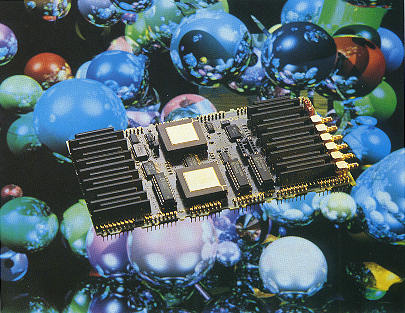
So in simple words: 32 inputs can be freely connected to 32 outputs. Great for large Transputer networks which can be reconfigured only by reprogramming the C004 – on top of that, you can cascade them and create huge, complex networks to make any connection imaginable possible. Like those Parsytec used in their SuperCluster machines looking like this:

MegaFrameXbarDetailYes, that’s 13 C004s and one Transputer to rule them all…

… so much for the theory.

In practice, the C004 is a bitch. Not only does it require a Transputer to configure it (normally a 16bit T2xx) it also adds quite a delay into the link-communication. As mentioned above, it’s “only a 1.75 bit time delay” but this can sum up to quite an amount.
Let me quote some more realistic numbers from the Helios manual (pp.255):

It is of interest to ascertain the effect of the Inmos C004 on the performance of the Helios communication mechanisms. Figure 6.3 illustrates the rates of data communication (Kbytes/second) attained using message passing primitives (PutMsg() and GetMsg()) between two Transputers that were
1. Directly linked and
2. Connected through a C004 link switch.
It is evident from Figure 6.3 that the effect of the C004 link switch on the rate of communication is far from negligible. The overhead imposed by the link switch increases with the size of the message. In the worst case (64 Kbyte message), transmission through the C004 is 23 % slower than sending data over directly connected links.

C004_helios

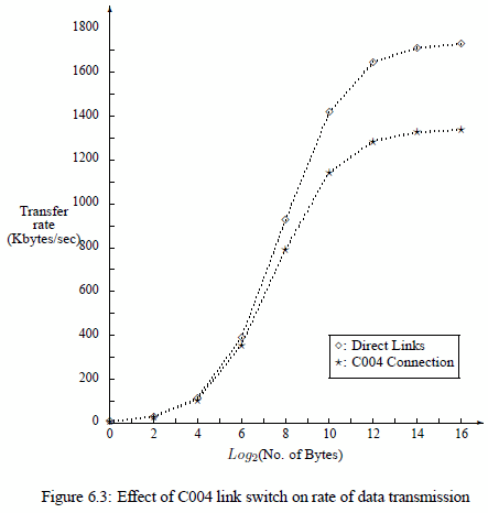
Oops. 23% is quite essential. So before planning to set up a crazy C004 network you might consider what you want to achieve.
Is it for educational network studies only? Fine.
Are you going for speed and rarely change your Transputer network configuration? Avoid it!

IMHO even the 10 possible Transputers on an IMSB008 do not require a C004 making your day.
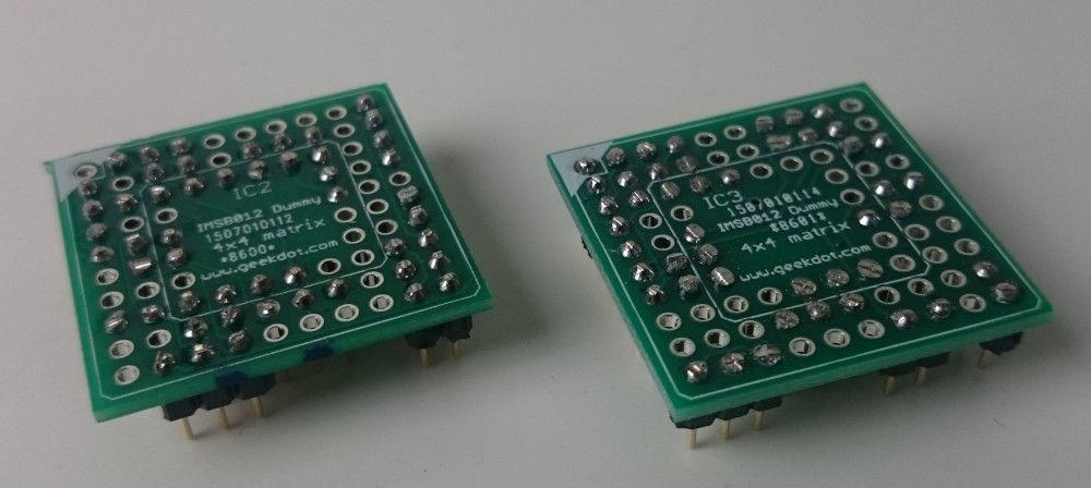
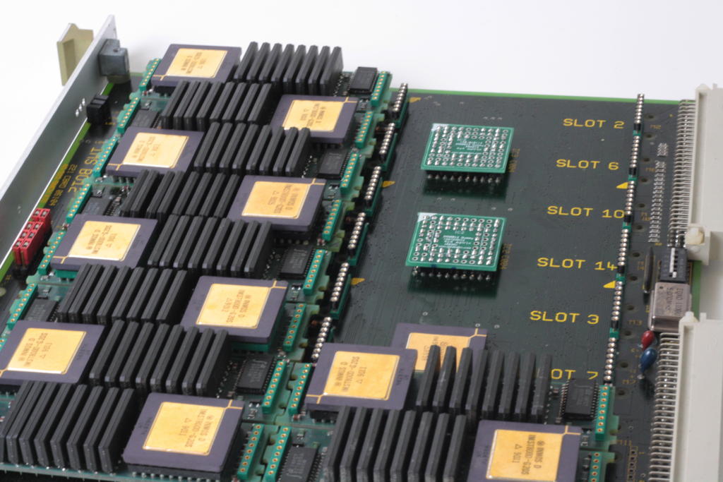
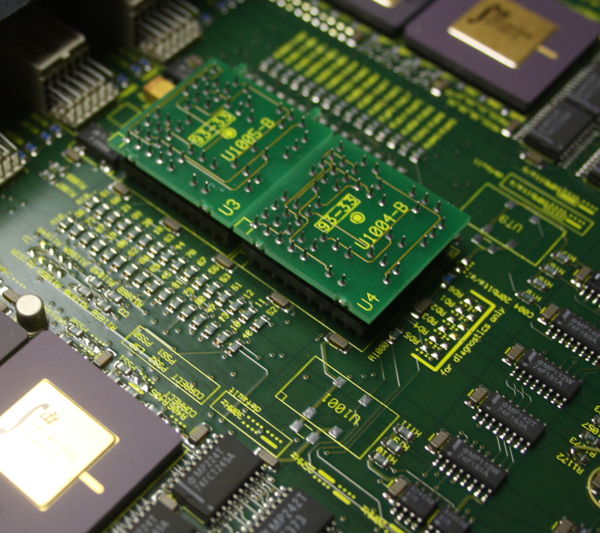
Actually, even Parsytec thought that this is useless to use a link switch for the 16 Transputers in their beautiful x’plorer and replaced it by hard-wire dummies:

C004_dummies2

Configuration

Ok, you’re still not scared away and really do like to know how to handle that beast. Fine, here’s what I went through:

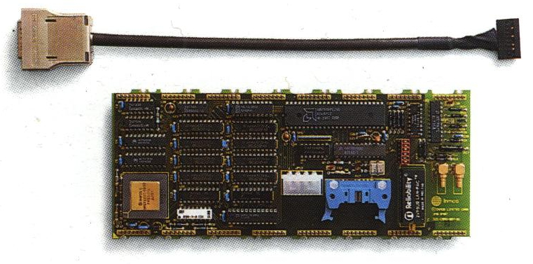
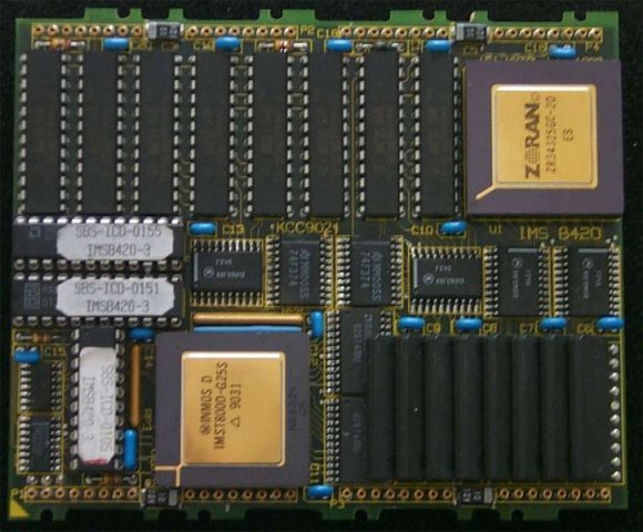
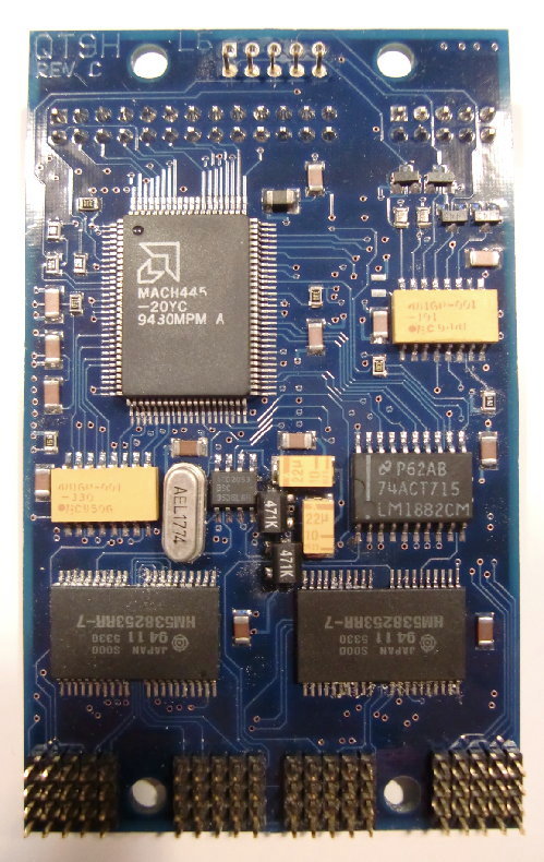
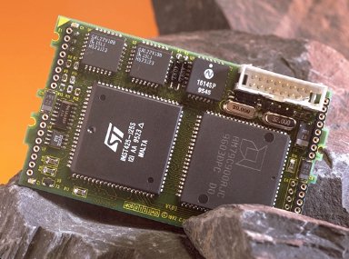
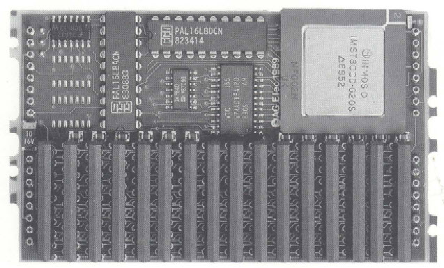
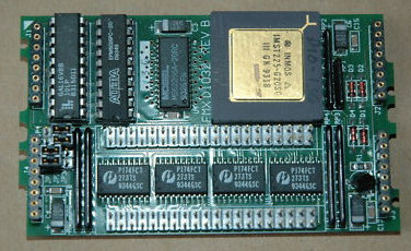
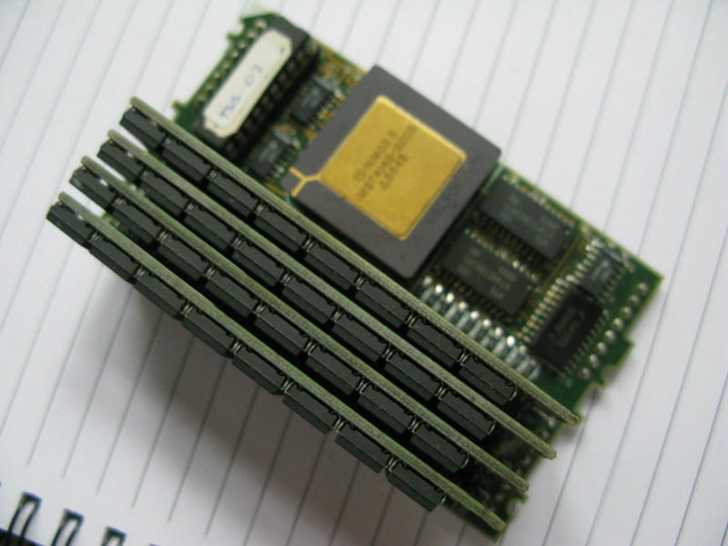
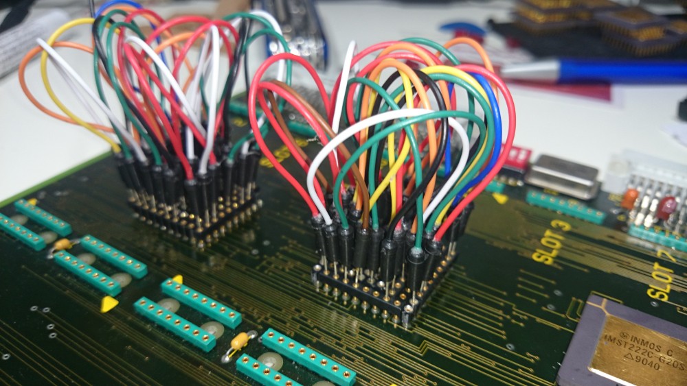
To work with a C004 you obviously need either a TRAM carrier like the B008 or some sort of motherboard like the IMSB012 or IMSB014.  Read the boards manual to understand how to connect to the T2xx Network Control Processor (NCP).
For example the IMSB012 has extra pins for “config down” (i.e. IN) and “config up” (i.e. OUT) for its T212 and any other boards being chained to it.
As for the IMSB008 has its T222 connected to Link 1 of TRAM 0.

The hardware wiring is important to know, because this information is needed for the so-called hardwire file used by the INMOS tool “MMS2” (Module Motherboard Software, MSDOS only, the manual is available here).
After reading the manual (do!) you should be able to read this hardwire file for an B008 quite easily. It describes the complete hardware setup and all physical connection between the C004(s), T2xx and Transputer/TRAM links on the board:

-- B008 hardwire description
DEF B008
  SIZES
    T2 1
    C4 1
    SLOT 10
    EDGE 10
   END
   T2CHAIN
     T2 0, LINK 3 C4 0
   END
   HARDWIRE
     SLOT 0,LINK 2 TO SLOT 1,LINK 1
     SLOT 1,LINK 2 TO SLOT 2,LINK 1
     SLOT 2,LINK 2 TO SLOT 3,LINK 1
     SLOT 3,LINK 2 TO SLOT 4,LINK 1
     SLOT 4,LINK 2 TO SLOT 5,LINK 1
     SLOT 5,LINK 2 TO SLOT 6,LINK 1
     SLOT 6,LINK 2 TO SLOT 7,LINK 1
     SLOT 7,LINK 2 TO SLOT 8,LINK 1
     SLOT 8,LINK 2 TO SLOT 9,LINK 1
     C4 0,LINK 10 TO SLOT 0,LINK 3
     C4 0,LINK 1 TO SLOT 1,LINK 0
     C4 0,LINK 11 TO SLOT 1,LINK 3
     C4 0,LINK 2 TO SLOT 2,LINK 0
     C4 0,LINK 12 TO SLOT 2,LINK 3
     C4 0,LINK 3 TO SLOT 3,LINK 0
     C4 0,LINK 13 TO SLOT 3,LINK 3
     C4 0,LINK 4 TO SLOT 4,LINK 0
     C4 0,LINK 14 TO SLOT 4,LINK 3
     C4 0,LINK 5 TO SLOT 5,LINK 0
     C4 0,LINK 15 TO SLOT 5,LINK 3
     C4 0,LINK 6 TO SLOT 6,LINK 0
     C4 0,LINK 16 TO SLOT 6,LINK 3
     C4 0,LINK 7 TO SLOT 7,LINK 0
     C4 0,LINK 17 TO SLOT 7,LINK 3
     C4 0,LINK 8 TO SLOT 8,LINK 0
     C4 0,LINK 18 TO SLOT 8,LINK 3
     C4 0,LINK 9 TO SLOT 9,LINK 0
     C4 0,LINK 19 TO SLOT 9,LINK 3
     C4 0,LINK 20 TO EDGE 0
     C4 0,LINK 21 TO EDGE 1
     C4 0,LINK 22 TO EDGE 2
     C4 0,LINK 23 TO EDGE 3
     C4 0,LINK 24 TO EDGE 4
     C4 0,LINK 25 TO EDGE 5
     C4 0,LINK 26 TO EDGE 6
     C4 0,LINK 27 TO EDGE 7
 -- Uncomment the next two lines if the
 -- patch header wiring is used to
 -- connect C004, link 28 to PatchLink0,
 -- and C004, link 29 to PatchLink1.
 -- C4 0,LINK 28 TO EDGE 8
 -- C4 0,LINK 29 TO EDGE 9
   END
PIPE B008 END

After that’s done, you can prepare a second file. The so called “softwire file” which actually tells the T2xx how to internally connect his in- and out-links. A very simple example would be:

SOFTWIRE 
PIPE 0
 SLOT 0,3 TO SLOT 1,3 
END

This would connect TRAM-0’s 3rd link to TRAM-1’s 3rd link.
Now that you have the necessary config files let’s move on to the MMS itself.

Software

As with nearly every software from INMOS the MMS too is written in OCCAM and therefore has to run on a Transputer. This might be the one in TRAM slot 0 on your B008 or on a local ISA board which itself is connected with 2 links to a B012 (one for config and one to the Transputer network).

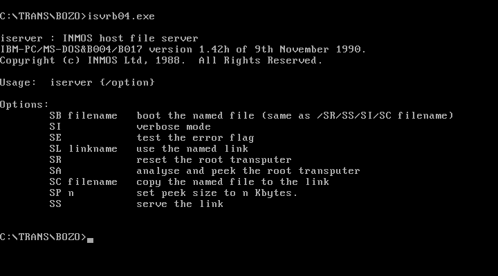
To make things easier, I prepared a complete MMS archive to download here (links to my Transputer Software page).
It contains some example soft- and hardwire files, an ISERVER.EXE (the program you need to upload code into your Transputer) as well as a batch file to easily start MMS (RUN_MMS.BAT).
Also you will find a folder with INMOS’ pimped version of ANSI.SYS called BANSI (“Better ANSI”), because all INMOS tools make heavy use of ANSI screen control. So put that into your CONFIG.SYS.

Before we begin, let’s have a look at my IMSB012 with ispy:

ispy 2.33
   # Part rate Mb Bt [  Link0  Link1  Link2  Link3 ]
   0 T800d-25 0.37 0 [   HOST    1:1    2:1    ... ]
   1 T2   -20 1.64 1 [    ...    0:1    ...    ... ]
   2 T800d-25 1.75 1 [    ...    0:2    3:1    ... ]
   3 T800d-25 1.77 1 [    ...    2:2    4:1    ... ]
   4 T800d-25 1.77 1 [    ...    3:2    5:1    ... ]
   5 T800d-25 1.75 1 [    ...    4:2    6:1    ... ]
   6 T800d-25 1.75 1 [    ...    5:2    7:1    ... ]
   7 T800d-25 1.75 1 [    ...    6:2    8:1    ... ]
   8 T800d-25 1.75 1 [    ...    7:2    9:1    ... ]
   9 T800d-25 1.75 1 [    ...    8:2   10:1    ... ]
  10 T800d-25 1.75 1 [    ...    9:2   11:1    ... ]
  11 T800d-25 1.75 1 [    ...   10:2   12:1    ... ]
  12 T800d-25 1.75 1 [    ...   11:2   13:1    ... ]
  13 T800d-25 1.77 1 [    ...   12:2   14:1    ... ]
  14 T800d-25 1.77 1 [    ...   13:2   15:1    ... ]
  15 T800d-25 1.75 1 [    ...   14:2   16:1    ... ]
  16 T800d-25 1.77 1 [    ...   15:2   17:1    ... ]
  17 T800d-25 1.77 1 [    ...   16:2    ...    ... ]

Ok, let’s start MMS2. Use/modify the batch “run_mms.bat” which will do all environment variables expected by iserver.exe and also adds the input and output files – change it as you please.
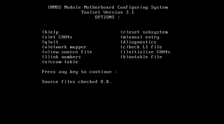
If everything works fine, iserver loads MMS2.B4 onto your Transputer and executes it. Your screen should look like the screenshot below.
First, I suggest you press “c” for checking the consistency of your hard/softwire files – if everything’s fine, MMS2 will print “Source files checked O.K.” as seen in the lowest line in the screenshot.

MMS1

Just for the fun of it, you can try MMS’ very own network worm – so press “n” to start the network mapper. You will see that it is much slower than e.g. ispy, so just be patient.
After some seconds, you should get something like this:

MMS2

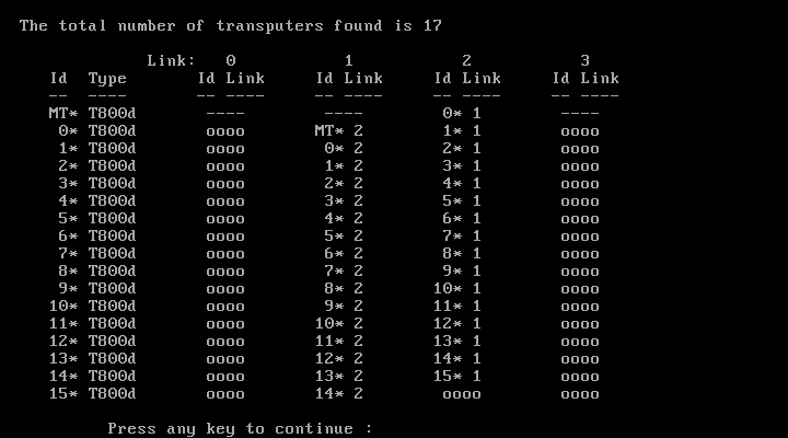
Now it’s time to program you network. So press “s” to set the C004(s). Some infos will rush trough the bottom line of the screen and finally MMS2 states “C004 setting preformed O.K.“:

MMS3

Nothing more to do here so press “q” to quit MMS2.  (Do not run the network mapper again! It seems to reset the T2 and in my case reproducibly crashes the network).
It’s better to use ispy. ispy v2.33 to be precise. I encountered several issues with the C004 and the most recent version 3.23 of ispy.

So running ispy including the /C4  switch to display the settings of the two C004s now shows this – mind all the new connections of each Transputers Link0 and 3:

ispy 2.33
   # Part rate Mb Bt [  Link0  Link1  Link2  Link3 ]
   0 T800d-25 0.37 0 [   HOST    1:1    4:1    ... ]
   1 T2   -20 1.74 1 [    2:C    0:1    ...    3:C ]
   2 C004b   [ 6S3JM54V --U8-1C- -G--F9-I T--7-PQ- ]
   3 C004b   [ -D-2650R BL--E--K H-N3--4- -TU-1OA7 ]
   4 T800d-25 1.65 1 [    ...    0:2    5:1    6:0 ]
   5 T800d-25 1.75 1 [    ...    4:2    7:1    8:0 ]
   6 T800d-25 1.41 0 [    4:3    9:2    8:1   10:0 ]
   7 T800d-25 1.75 1 [    ...    5:2    9:1   11:0 ]
   8 T800d-25 1.41 0 [    5:3    6:2   11:1   12:0 ]
   9 T800d-25 1.75 2 [    ...    7:2    6:1   13:0 ]
  10 T800d-25 1.35 0 [    6:3   13:2   12:1   14:0 ]
  11 T800d-25 1.41 0 [    7:3    8:2   13:1   15:0 ]
  12 T800d-25 1.42 0 [    8:3   10:2   15:1   16:0 ]
  13 T800d-25 1.32 0 [    9:3   11:2   10:1   17:0 ]
  14 T800d-25 1.35 0 [   10:3   17:2   16:1    ... ]
  15 T800d-25 1.41 0 [   11:3   12:2   17:1   18:0 ]
  16 T800d-25 1.33 0 [   12:3   14:2   18:1    ... ]
  17 T800d-25 1.32 0 [   13:3   15:2   14:1   19:0 ]
  18 T800d-25 1.35 0 [   15:3   16:2   19:1    ... ]
  19 T800d-25 1.32 0 [   17:3   18:2    ...    ... ]

Yay! It worked. Positively as well as negatively.
Besides the new connections you might also spot a difference in the link-speed column. In our first run of ispy all Transputers had a link-speed around 1.75MBps.  Now it varies between 1.75 and 1.32, depending on how often the ispy worm crossed a C004.

Two final hints:

If your C004 network has been set-up as planned, you can use ispys output to programm the network later.
Just save the output into an ASCII file (ispy /c4 > my_net.txt) and when needed feed it back into ispy like this:
 ispy /r /cr < my_net.txt
This will reset the network and read in the configuration from stdin.
Obviously you can also manually edit the text file, the c4 lines

   2 C004b   [ 6S3JM54V --U8-1C- -G--F9-I T--7-PQ- ]
   3 C004b   [ -D-2650R BL--E--K H-N3--4- -TU-1OA7 ]

which isn’t as comfortable and comprehensible as editing a hard/softwire file. But your mileage my vary.

Alternatively, MMS2 can create a bootable file with your network settings. This can be used for quickly setting-up your system.
Just hit the “b” key and enter a filename. My MMS2 archive contains the above example as “BOOTB012.BTL”. Run it with “iserver /SB bootb012.btl“.

Caveats

Mind your reset! This means, in many cases a root Transputer might reset all the “worker Transputers” but also your T2xx and in effect all C004. So be careful when resetting your system.

Yes, theoretically you can reconfigure your Inmos C004 on the fly while all connected Transputer run. The most prominent example is having one network topology during data acquisition while changing it for number crunching later on.
This requires a very good knowledge of the notwork and thorough process locking etc.

Basic Transputer Tools

Ok, so you have your shiny (not so) new Transputer system installed/connected and you really like to know if it works and at least see some results… you’re in need of basic Transputer tools to get started.

First, download the Geekdot “Transputer Tool Kit” from my Transputer software page (New releases are possible, mind the version number).
Each tool introduced here has its own folder in the archive.

ispy/mtest

Even it’s historically not the first application ever developed for Transputers it’s for sure one of the most used.
It started as ‘check‘ and at some point got renamed into ‘ispy‘ – whatever the name is, the technical term would be “network worm”. This means it’s a special piece of code which a) sniffs around in a transputer (what kind, number of links and their speed) and b) replicates itself over all links it previously found.
When done, it outputs a network map like this example:

Using 150 ispy 3.23
 # Part rate Link# [ Link0 Link1 Link2 Link3 ] by Andy!
 0 T800d-25 292k 0 [ HOST   ...   ...   1:0  ]
 1 T425c-20 1.6M 0 [  0:3   2:0   3:0   ...  ]
 2 T400c-20 1.8M 0 [  1:1   ...   ...   ...  ]
 3 T400c-20 1.7M 0 [  1:2   ...   ...   ...  ]

ispy is used on geekdot.com extensively, so any time I write about Transputers you will see some sort of ispy output for sure.
There are several versions of ispy included in this kit. This is because some versions behave more stable than other in certain circumstances. E.g. the most recent version 3.23 does not work very well with the C004 link-switches.

“The other part” of ispy is called mtest. mtest takes ispys output and runs an indepth memory test/report on all Transputers found.

iserver

iserver is part of what INMOS called “itools” – long before Apple discovered the “i” for themselves 😉 – there were many others, mainly development focused (e.g. idebug, icconf etc.).
It is more or less the successor to the godfather of all Transputer booting tools “afserver” (1988). Well, it has to be, being the on INMOS supplied with all their other tools and languages.
The possible options are quite self-explanatory and printed to stdout when omitting any option:

iserver142h

Basically if you see a *.btl, *.b4 or *.b8 file it’s most likely meant to be executed with iserver. Before running successfully iserver need some environment variables set to successfully to be used:

set IBOARDSIZE=#100000
set TRANSPUTER=#150

These two settings tell all itools how much RAM the Transputer has to work with and at which port address it can be found (0x150 is default anyway). The archive contains V1.42h from Nov. 1990 which is the most recent as far as I know.

Mandelbrot

The “CSA Mandelzoom Version” is one of my favorite benchmark tools. I like it so much, that I run it once a while just for fun.. and to extend my benchmark table which I’ve collected over the time using it.

It is nice because it features integer (T4xx) as well as floating point (T8xx) versions of the calculation ‘slave processes’ and scans the network itself. No external tool needed. It’s also possible to let the host (i.e. your PC) calculate the Mandelbrot fractal to get an idea, how much faster/slower your Transputer network is – the archive contains a little benchmark result text file which I accumulated over the years.
Also there are some handy switches available (‘-h’ for help):

  • -v : Use VGA graphics
  • -t : Run on host instead of Transputers
  • -a : Autozoom, loads  a list of coordinates from man.dat and start calculating them without manual interaction.
  • -b : Use a different base address (instead 0x150)
  • -x : Verbose output of the Transputer initialization process (added by me)

After a while I got tired of manually time a calculation run and also ran into problems with large networks which simply became to fast to hand time. So I extended the code of Mandelzoom with a high precision timer (TCHRT, shareware, can’t remove the splashscreen, sorry) which prints out a timer summary when run with the “-a” parameter. I provided my default “MAN.DAT” file, which contains 2 coordinates to calculate (1st & 2nd run) and used for all my benchmarks.

csa_mandel_timerThese are the results of my DOS host system running in VirtualBox.

Caveat: It breaks if there’s a T2xx in the network (e.g. B008/B012) 🙁 And as always: Read the F-ing README.txt!

Since I started to heavily modifying the source, I wrote a post of its own about it as well as put everything on github, so you can join the fun 😉

Other Tools

iskip

iskip can be very handy, when ‘talking’ directly to (externally) connected links, e.g. another network which is connected to your root Transputer. Here’s a good example:
You like to put code directly onto “processor 1” which is connected to link 2 of your root Transputer:

iskip

So you call

iskip 2 /r /e

This sets up the system to direct the program to the target network over the top of the root transputer and starts the route-through process on the root transputer. Options ‘R’ and ‘E’ respectively reset the target network and direct the host file server to monitor the halt-on-errorflag. The program can then be loaded ‘through’ the root Transputer directly onto processor 1 using:

iserver /ss /se /sc test.btl

debug.exe

Yes, I do mean the comes-with-DOS debug.exe. Well, you can use any debugger you like as long it can read/write to port addresses.
Obviously this means [MS|PC|Open|Free]DOS only. You won’t get far with this on Linux, any Windows or OS/2. At least for initial debugging and testing I strongly recommend to use the “bloated interrupt manager” known as DOS.
First of all, you have to know the port addresses the C012 registers are mapped to . There’s a de-facto industry standard which INMOS introduced with the IMSB004. Its been adopted by 90% of all 3rd party products, even with certain ISDN cards using Transputes.

The base address normally is at 0x150 (which can be configured to other addresses in some cases). From this base adress the offset is always the same:

Base Adress Register Comment
+0x00 C012 input data  read
+0x01 C012 Output data write
+0x02 C012 input status register read = returns input status
write = set input interrupt on/off
+0x03 C012 Output status register read = returns output status
write = set output interrupt on/off
+0x10 Reset/Error register write: Reset Transputer & C012 and possibly subsystem (check manual)
read: Get Error status
+0x11 Analyse register  (un)set analyse

So here’s a clean Transputer setup ‘conversation’ using debug (comments are just for clarity, not supported in debug):

c:\>debug
 -o 160 1         # Assert RESET
 -o 161 0         # Deassert ANALYSE
 -o 160 0         # Deassert RESET ... init B004/IMSC
 -o 152 0         # Clear Input  Interrupt enable
 -o 153 0         # Clear Output Interrupt enable
 -i 152           # Read Input Status
 00               # Bit 0 = 0 -> no Data waiting
 -i 153           # Read Output Status
 01               # Bit 0 = 1 -> ready to send 
 -i 160           # Read Error
 00               # Bit 0 = 0 -> ERROR not signaled
-o 151 1          # send POKE
-i 153            # Read Output Status
01                # Ready -> POKE Ack (00 = BAD no Transputer) 
After that you’re fine to send and receive bytes through 0x151/0x150. Doing so, you’re completely free which programming language to use. Here are some examples in AppleSoft Basic or even Python.

IMSB012 C004 replacement

The IMSB012 is my favorite TRAM carrier board. Room for max. 16 (size-1) TRAMs and plenty of external connectors. The perfect platform to build a successor of the ‘Tower of Power’.

Like with all TRAM carriers having more than 8 slots, it was a good decision to put at least one C004 link-switch onto the board.
While that’s generally a good feature, you (and me) might not need the option to reconfigure your Transputer network several times a week… And if you’re completely sure how you like your network it would be better to set if once and for all without the signal delay penalty you have to pay using one or even two C004s.

So in my case, I’m perfectly fine with the 4×4 matrix mentioned in the B012 manual (and also used as an example in my C004 post). So instead of using the clumsy MMS tool and having an extra link used into the T212, I planned tp remove the T212 and the two C004s and replace them with two dummies. Pretty much the same way like Parsytec did it with their x’plorer.
First I had to chew myself through the B012 schematic to understand the connection of each TRAM slot into the C004s. After that it was time for some intense cable plugging:

C004 dummy test

If you plan to do so, please be aware that the socket holes are too thin for a normal (0.63mm?) jumper cable. You might ruin your socket if you use force to plug them in!
I created a interpose socket by using single row pin header sockets which itself had thin enough pins to fit into the original B012 socket.

After some corrections, the buzzing-through of all 16 slots went fine and the schematics went to the PCB house (I have some PCBs left, ask for a quote if you need some).

And this is how the C004 replacement PCBs look when completed:

IMSB012 C004 dummies

Again, to solder in the pins, you’ll need really thin ones. Thinner than 0.5mm that is. Also, you don’t need to populate all 84 pins, I only use 51 per dummy (bridging some gaps).

Additionally, I strongly advise to isolate each dummy’s top with some kind of tape to avoid (electrical) contact to the TRAM placed above it. This is how they look seated on the B012 underneath slot 6 and 14 – the T212 under slot 7 not yet removed:

in_IMSB012