Category Archives: TRAMs

Inmos TRAMs

INMOS was obviously the first manufacturer of TRAMs. Over the time you can clearly see the progress the technology made over the period Inmos TRAMs were made. Starting with comparably big sizes, using DIP chips etc. the last of its breed were highly integrated PCBs cramped with SMD parts and chips.

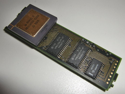
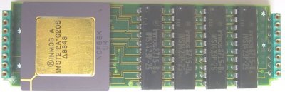
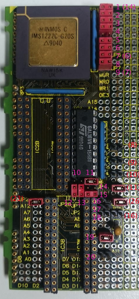
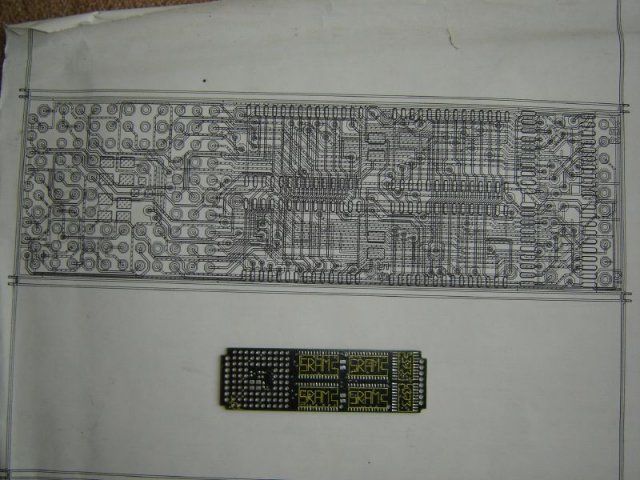
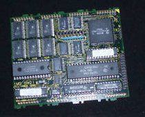
The IMS B401 started it all. A 32KB SRAM size-1 TRAM for a 32-bit Transputer. Here’s the prototype, the final product and a picture of its schematic:

B401_Layout

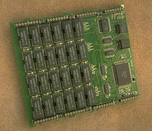
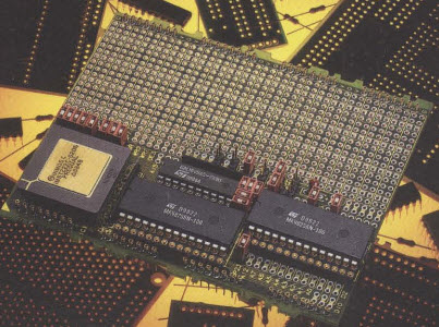
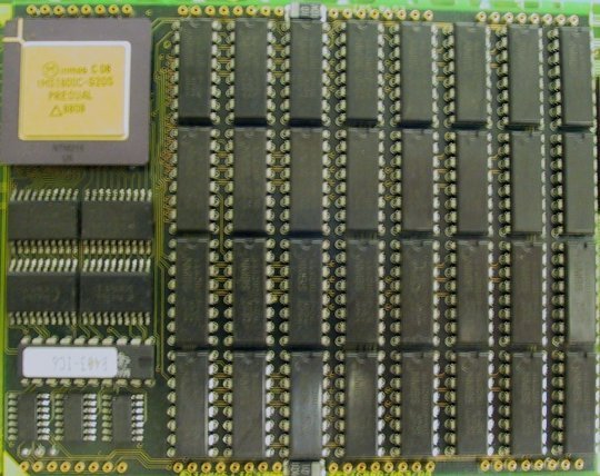
The “huge” IMS B403 1Mbyte DRAM Size-4 TRAM:

IMSB403_1

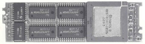
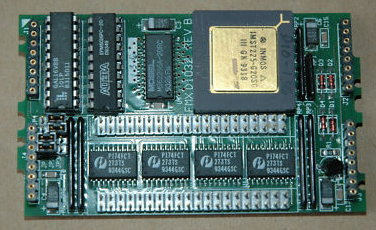
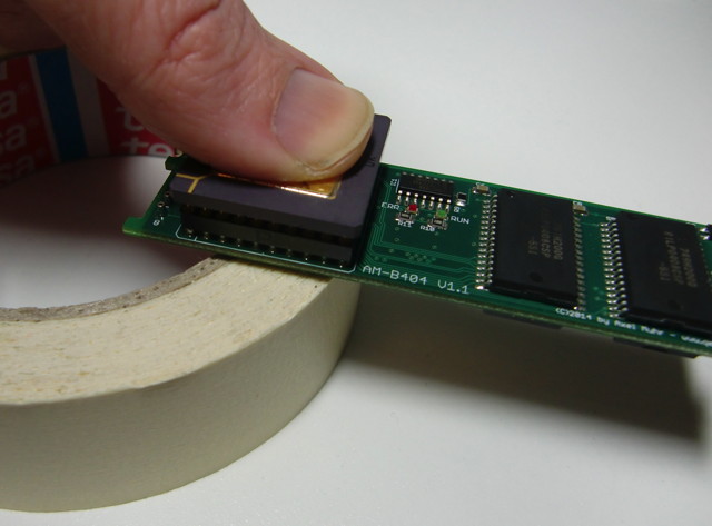
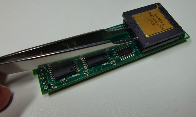
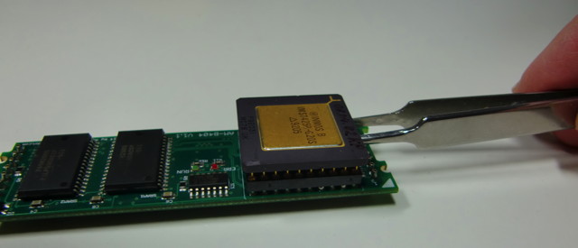
The IMS B404 (2MB DRAM, Size-2) is where the fun starts. Size-2 is just OK not to totally hog your mainboard and 2MB is what you need for OCCAM or HELIOS to make something useful.
Actually, the B404 has 3 “levels” of RAM. 4K internally in the Transputer, 32K SRAM and 2048K DRAM. As they are superimposed (i.e. overlapping), the total amount is still 2MB with different access speed at 0-4k (1 cycle), 5-32k (3 cycles) and 4-5 cycles above.

IMSB404

There were also the IMSB402 (8Kbyte Size-1) and the IMSB405 8Mbyte Size-8 TRAMs of which I have no pictures yet.

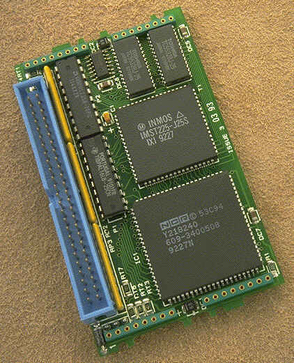
The IMS B407 was an Ethernet TRAM (Size-8!), proving that a TRAM doesn’t need to be necessarily a Transputer Module for number crunching only.

imsb407

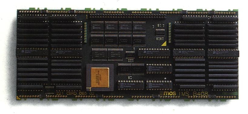
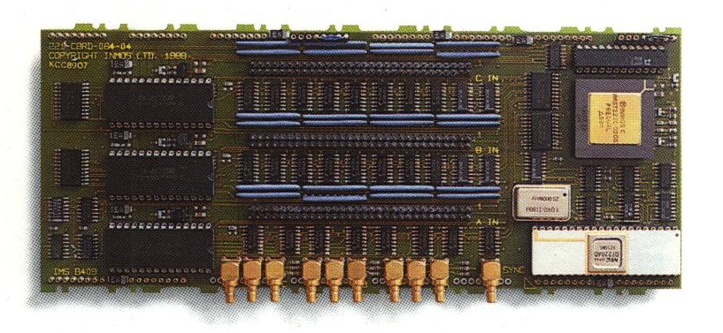
The IMS B408 and B409 were both part of a graphics system, so you didn’t the to have the host to render the graphics – which would have been much slower than those TRAMs.
The B408 was the “drawing pad image storage” (1,25MB dual-ported RAM), while the B409 had the timing generator and the CLUTs:

imsb408

imsb409

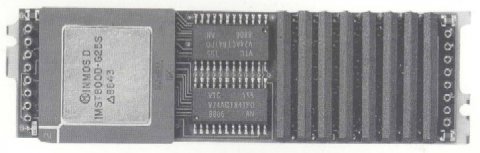
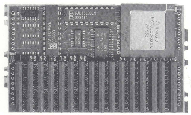
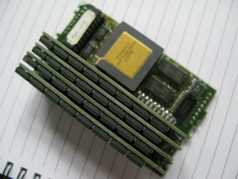
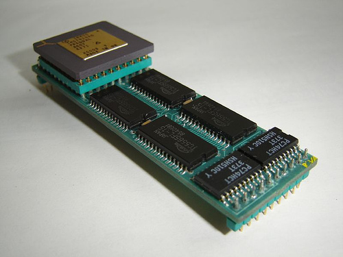
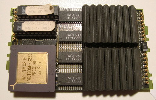
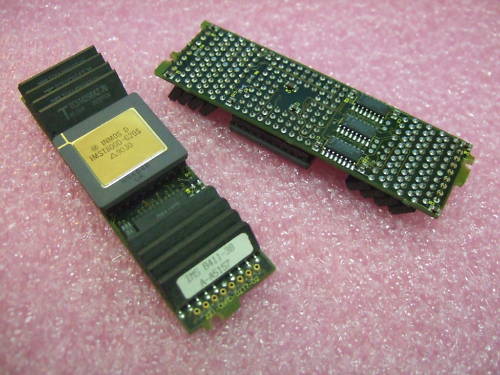
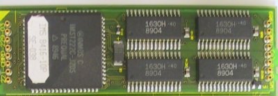
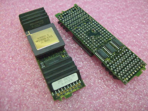
The IMS B411 can be seen as a new era: 1MB DRAM on just a size-1 TRAM made possible by the use of small ZIP-packaged DRAMs… which were very expensive, of course.

IMSB411-3B

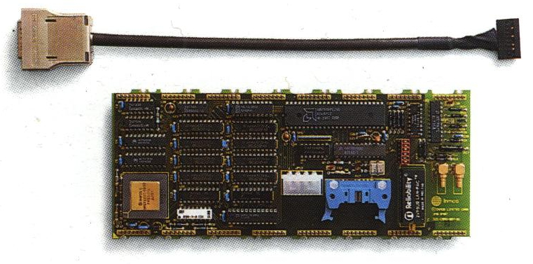
The IMS B415 is a simple Transputer-Link to RS422 converter. This way, link connections can span up to 30 meters.

imsb415

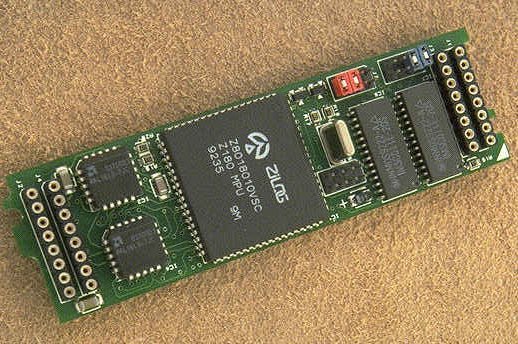
The IMS B416 features a 16bit T2xx Transputer and 64KB SRAM

IMSB416_10P

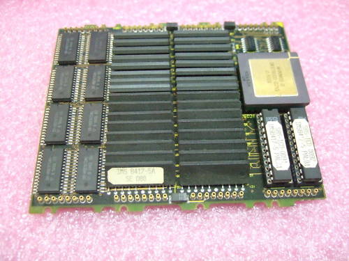
The IMS B417 is a massive beast: 4MB on a size-4 TRAM… well, still better than the B403.

IMSB417-5A

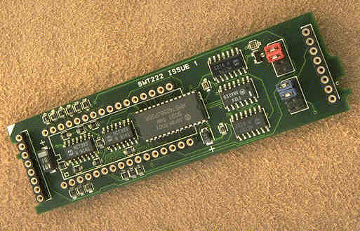
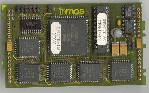
The IMS B418 contains a 16-bit T222 and 256KB Flash ROM… quite modern stuff those days and probably a good way to boot your HELIOS system from 😉

IMSB418_1

The IMS B419 combined the two huge B408 and B409 modules into one size-6 TRAM. A nice graphics TRAM with 2MB DRAM and 2MB VRAM…

imsb419

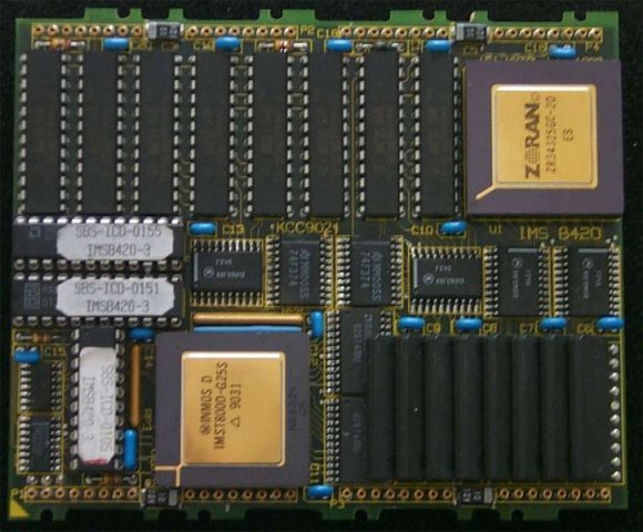
The IMS B420 featured a ZORAN ZR34325 DSP (45 MFLOPS peak) with its own 256KB SRAM besides the obvious T800 Transputer and 4MB DRAM. My guess is, that it is comparable to the Quintek QVA-T TRAM.

imsb420_1

The IMS B421 enabled a Transputer system to talk to GPI/IEEE-488 buses … like laboratory equipment or your old Commodore Floppydrive 😉

IMSB421_1

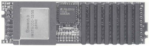
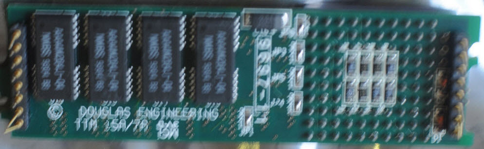
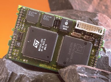
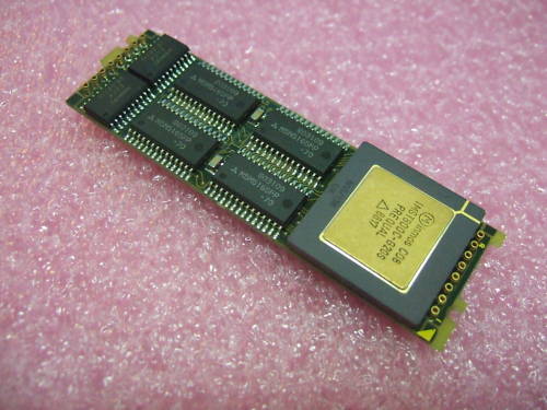
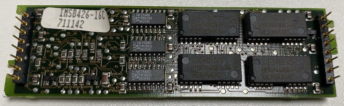
Ahh, the real-deal… the IMS B426 is what you want in your TRAM collection. 4MB RAM on a size-1 TRAM. This is where Helios really loves to run on.

IMSB426-5A

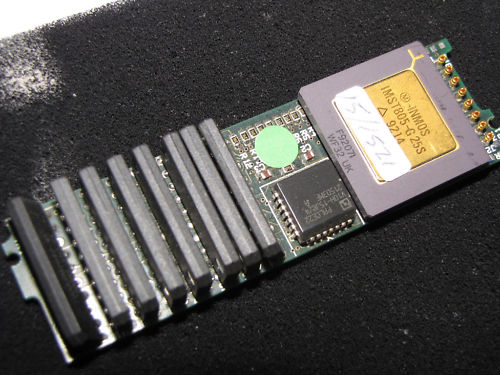
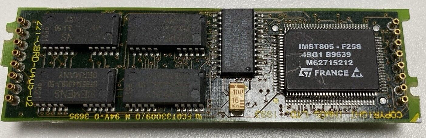
…and here’s a more recent version of the B426 (rev “-16C”, 1993), this time all SMD, featuring the latest T800 in a nice TQFP case

IMS_B426

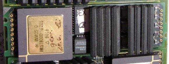
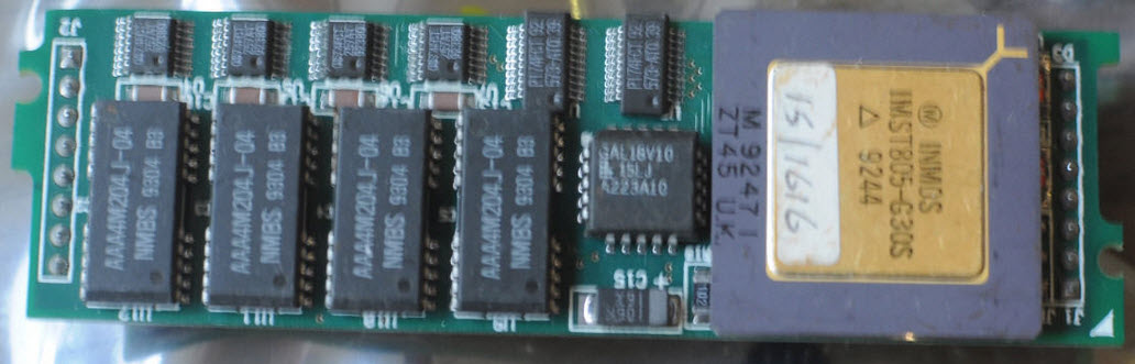
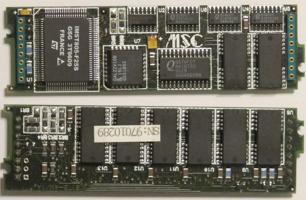
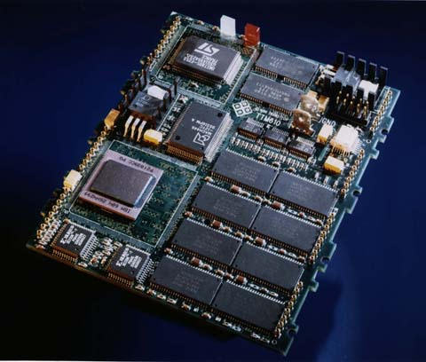
Well, the IMS B426 is great… as long as you can’t get the IMS B427 😉 This Size-2 TRAM features a whopping 8MB RAM. Enough for running Helios and X11 on it.

IMSB427

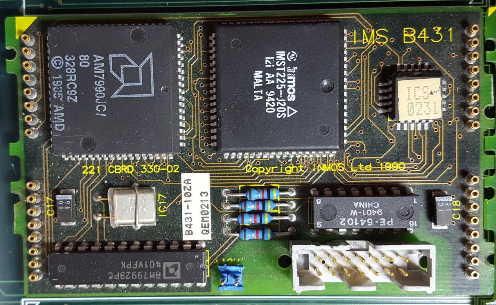
Something more important than ever is a fast network connection. The last ethernet TRAM from INMOS was the IMS B431.
10mbps is the maximum you get… well, more wouldn’t make sense given the Linkspeed of 20mbps.

IMSB431

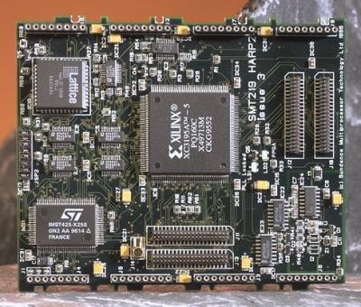
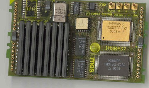
The IMS B437 is a very neat little thing: A graphics TRAM as size-2 TRAM! A nice 25MHz SMD T805 and a G332 colo(u)r video controller. Rare as chicken teeth!
It looks like this was designed by Contex Systems Design Ltd. and OEM’ed by INMOS.

IMSB437_1

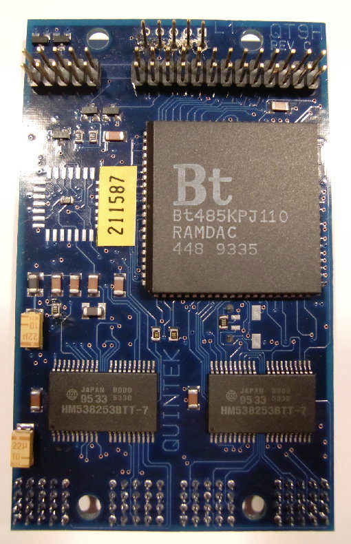
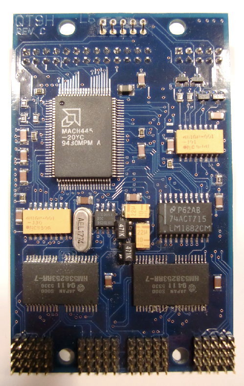
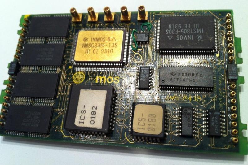
And when you thought you’ve seen them all, another one pops up:
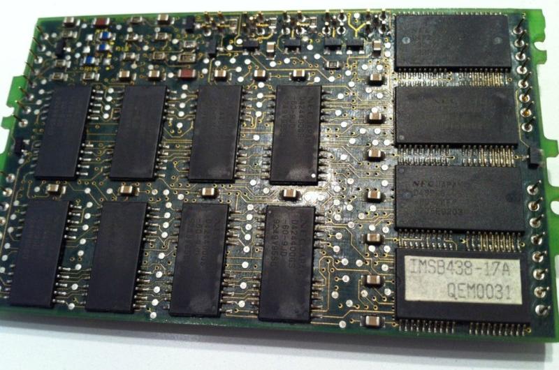
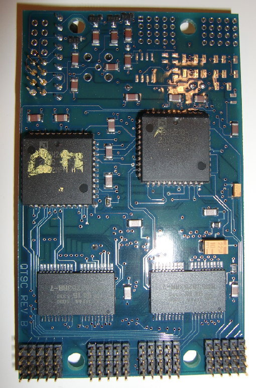
The mighty IMS B438. As the name-code suggests, it’s an updated B437 – very updated and IMHO the ultimate graphics TRAM: 2MB VRAM, 4MB DRAM, 30MHz T805 and the last and final 32Bit video controller G335@130MHz. I really, really want one. Badly!

B438

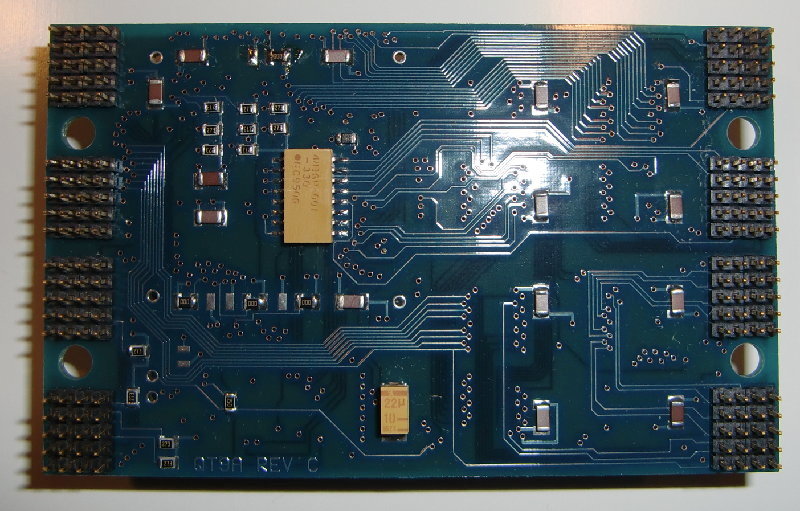
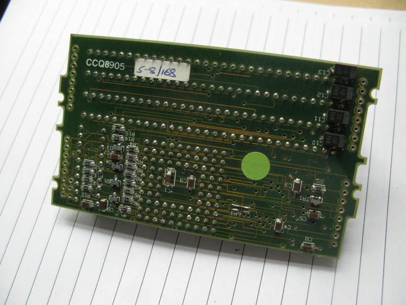
Because it’s a beauty, here’s its back, too:

B438_back

HTRAMs

As the T9000 had so many new features and architectural differences the “classic” TRAM wasn’t enough to support all that. So INMOS went to enhance the TRAM-model…

And they meant it! Instead of DIL 16 Pins of a “classic” TRAM, HTRAMs could use up to 160(!) pins to communicate to the outside world. Besides the classic 5V, also 3.3V was supplied on one pin as a tribute to the technical progress. Due to the introduction of the DS-Links (vs. OS-Links within the T4xx familiy), each of the four links of the T9000 now required 4 pins per link, resulting in 16 pins for the links alone. Plus many other special links for Events, ConfigUp/Down etc. a minimum of 60 pins were used.
Also each HTRAM now featured a PROM so it could be identified by software.

This is the pinout of an HTRAM extracted from the most recent source (SGS-Thomson B92x HTRAM datasheet, Nov. ’94)

HTRAM

Pin Row a Row b Row c Row d Row g Row h
1
2
3
4
5
ClkIn
L0SIn
L0DIn
L0DOut
L0SOut
N/C
GND
N/C
V3V3
N/C
TDI
V5V0
CupSIn
GND
CUpDIn
notTRST
L2SOut
L2DOut
L2DIn
L2SIn
EventIn0
EventIn1
EventIn2
EventIn3
EventOut0
EventOut1
EventOut2
EventOut3
9
10
11
12
13
L1SIn
L1DIn
L1DOut
L1SOut
Reset
N/C
V5V0
N/C
GND
TMS
CUpDOut
GND
CUpSOut
V3V3
TCK
L3SOut
L3DOut
L3DIn
L3SIn
V5V0
1
2
3
4
5
N/C
N/C
N/C
N/C
N/C
TDO
GND
CDnSOut
V3V3
CDnDOut
9
10
11
12
13
N/C
N/C
N/C
N/C
N/C
CDnDIn
V5V0
CDnSIn
GND
N/C

While many (i.e. 100) pins left unspecified in this pinout-map (e.g. Block 2 rows c & d, Block 3 rows e & f and the complete Block 4), they’re all used on the HTRAMs I own.
My guess is that those were used for the memory-bus, at least in the case of my Quintek board.

Here’s an original INMOS HTRAM, with a 15MHz T9000 engineering sample mounted, plus a T9000 (backside) next to it:

HTRAMandT9k

For a quickstart here are the 3 HTRAMs from Quintek which I own:

QT9A

The QT9A (Rev.C in this case) is a processor HTRAM of (yet) unknown clock-speed and memory-size – I think it’s 4MB. Because the T9000 ran really hot in the prototype stage (which he never left), all of them required a compariby big heat-sink. I do not dare to remove it, given the (collector) value.

QT9A_front

…and the backside for completeness 😉

QT9A_back

QT9H

This is a display HTRAM featureing a Bt485 RAMDAC, 2MB VRAM but no video-output part. The video signal is delivered to a pin-row which is going connected to a VGA-featurebus on a graphics card. It’s a Rev.C part, like the QT9A.

This and the following HTRAM were fitted into Slots 5 and 5 on the HTRAM-board which are quite special slots: They don’t offer the pin-blocks 1 & 2, i.e. no DS-Links etc.! That said they do feature fully populated pin-blocks 3 & 4 which underlines my assumption that those pins are meant for direct memory-mapping.
In the case of a Video & Encoding HTRAM this makes totally sense because it gives the Transputer even faster access to the Video-RAM than pumping all the data over the Links.
Which leaves yet-another-riddle-to-be-solved: Where are those HTRAM mapped into the T9000s memory?

QT9H_front

…quite a lot is happening on the back-side, too:

QT9H_back

QT9C

A video digitizing HTRAM using the BrookTree/Conexant Bt812 chip and having 2MB VRAM, too… this time “Rev.B”.

QT9C_front

and the back side…

QT9C_back

To be continued…

3rd party TRAMs

Well, INMOS wasn’t the only company manufacturing TRAMs. This is a -more or less random- collection of TRAMs I was able to find in the WWW.

Because some TRAMs are of unknown origin, I’ll sort them by size…

Size-1 TRAMs

This is my 2nd smallest TRAM by RAM size. 128KB SRAM. The silk-print says “TRAM-1-B” on the front and “TRAM-1-L” on the back. I guess they’re made in Germany as it’s usual to mark the front with B (“Bauteilseite”, component-side) and L (“Lötseite”, solder-side).

TRAM1_32k

This seems to be a very early design, featureing a 16-bit T212 and some original INMOS SRAMs

Unknown_T212A_Module

This is my “standard 1MB” TRAM. It’s labeled “ARADEX T805S“. It seems that the German ARADEX AG, originally manufacturer of cardbox packaging machines built their own TRAMs for their systems. It’s pretty highly integrated. Some but not all of them feature an ALTERA EMP5016 PLD which hold extra logic for the additionally fitted subsystem pins..

ARADEX_T805S_1M_1

Transtech was a quite big manufacturer of all-things-Transputer. They had a big range of TRAMs in their catalogue. Pictured below are the TTM-1 (32KB SRAM), TTM-3 (1MB DRAM) and its successor TTM-7(1MB DRAM).

Transtech_TTM1

Transtech_TTM3

Transtech_TTM7

Here’s another image of which I think it’s an TTM7:

UnknownT1_1MB

The final TRAMs of Transtech were the TTM15(e) and TTM19(f), both using the SMD package of the T800 as well as the rest of the ICs.

The TTM15E uses some interesting “Enhanced DRAM” from Enhanced Memory Systems Inc.. These include 2K SRAM in each 4Mbit DRAM chip, which increases the access speed to 12ns.
Very neat, very hard to get-by today. Restoration impossible. Mind all the jumpers on the backside – obviously a lot is configurable here.

TTM15E

The TTM19F uses what looks like modern (S)DRAM – need to evaluate that more…

TTM19F

This is a special one: Two Transputers but no RAM. It’s labeled Alcor 2T. Very nice if you need lot’s of CPU-power and can live with the 4K RAM inside the Transputer.

Alcor_2T_no_memory

Sundance was another manufacturer concentrating on the Transputer business. They made lots of TRAMs, this SMT213 is comparable to the Alcor 2T but features two T805 Transputers in SMD as well as 1 or 4MB DRAM per Transputer (on the back) and was built in 1993 which is near the end of the Transputer era. With 4MB I’d consider this to be the “Rolls-Royce of the TRAMs”. Yummy!

Sundance SMT213

The SMT222 is an EPROM boot TRAM. You can see the socket for a 64-512KB EEPROM, inside the socket is a C011 to provide the DS-Links to the Transputer network.

Sundance SMT222

This is the SMT220, Consisting of a Z80 compatible micro controller (Z80180), a 32KByte SRAM data buffer, 512bytes of firmware and two C011 Link adapters, this TRAM is what I call an “RS232/485 interface overkill” – but I guess some industrial use required that.

Sundance_SMT220


Another TRAM, using seldom used AAA4M204 SOJ DRAMs (4x1Mbit). The label says “Douglas Engineering TTM 15A/7A” (Not sure about the last number given the blurred picture I found).
This one is interesting  in so far, that it is more or less a standard SIMM-on-a-TRAM. This would make a worthwhile retro-project to recycle all those 30-pin SIMMs sleeping in our drawers 😉

DouglasEng_TTM15a_front

DouglasEng_TTM15a_back

MSC (“Microcomputers Systems Components GmbH”) another pretty much unknown Transputer device manufacturer from Germany also made a SIMM-style TRAM and called it the B1T8-4M/A1.
As with the TTM15E, some settings can be configured by jumpers on the backside.

MSC-B1T8-4M_1A

Size-2 TRAMs

Next up, the STM228, a SCSI TRAM… something you want to get the most performance out of Helios or file-through-output in general.

Sundance SMT228 SCSI TRAM

The SMT229 would be the other TRAM you want for a professional system. This is the most modern ethernet controller available.

Sundance SMT229 Ethernet TRAM

The Transtech TTM-6 is a comparably boring 2MB computing TRAM. It’s an older design, like the IMS B404.

Transtech TTM6

This seems to be some sort of I/O TRAM… lots of 74FCT buffers and a T225. It’s called FMX D1032.

FMXD1032

This is an interesting one: A TRAM of unknown origin using SIPPs – as memory(-expansion)!

Very cool, as you could expand its RAM up to 64MB given all addresslines are used. Downside is that this TRAM is building pretty high…

TRAM_mit_SIMM_F

and the back:

TRAM_mit_SIMM_B

Size-4 TRAMs

We’re now coming to the “Big Guns”. Starting with TTM11, another SCSI interface. It’s older than the nice SMT229, so it only has a 16-bit T222 and some old SCSI controller (my guess it’s a WD93xx chip).

Transtech TTM11

This is the Sundance SMT214, a “large memory TRAM”. It was available with 16, 24, 32 or 64MB DRAM including a T805 at 25MHz. This should be sufficient for every Transputer application… as long as nobody ports Windoze to Transputers 😉

Sundance SMT214

The SMT219 was the commercialized version of the HARP1 project, called HARP2 then. It’s a T425 Transputer connected to an FPGA which could be programmed for any task you needed to get done… a C64 emulator for example 😉

Sundance SMT219

This is where it starts getting funny. Because Inmos was struggling with the next Transputer generation, other CPU manufacturers presented new quite fast  competitors, like the PowerPC from Motorola. This Transtech TTM610 featured not only a T805/25 but also a 200MHz PPC603 or 604 with 16 or 32MB of RAM.

TTM610 PowerPC TRAM

Parsytec thought the same and presented the ‘PowerTRAM’, an 80MHz PPC601 on a TRAM. Well, and there’s a T425/25, too.
If you like to know more, the Parsytec PPC systems have their own post over here.

Size-6 TRAMs

This is an graphics TRAM from “Division Ltd.” probably called DBT020/01. It features a T425 with its own 1 or 4MB RAM and 2 Toshiba TC8512 “Gouraud shading processors”, some VRAM and most likely an Inmos IMS Gxxx graphics controller.

DBT020 - unknown graphic TRAM

Size-8 TRAMs

This huge beast is a TTM220 with 16 or 32 MByte DRAM coupled to both an Intel i860XP  processor, and a T805 transputer. There was a bit smaller (size-6) version called TTM110, too.
All in all it provided the same features like the DSM860 cards (well, despite the 32bit Transputer).

TTM110 TTM220 i860 TRAM

(To be continued)

Handling TRAMS

General caveats

TRAM pins are thinner than normal PCB-Pins e.g. those you may know from Arduino shields and thus they are, well, quite fragile. That’s a problem (by design) with all TRAMs. So be very careful when handling TRAMs, i.e. removing/plugging them from/into your TRAM carrier e.g. a IMS B008.

And you can’t repeat this enough: Ground yourself! Electrostatic discharge will kill your TRAM as well as any other electronic device.

How do I do it? My main and single tool for handling TRAMs is this pair of straight tweezers:

Pliers

This works quite well for carefully removing TRAMs from its socket by putting it between TRAM and socket like this and gently lever the TRAM – not too much! Else you will bent the pins on the other side – repeat on the other side. Done.

The Transputer

If you got you TRAM without a Transputer plugged in, you might figure that it’s quite difficult to plug in the CPU. My suggestion:

Put the back of the TRAM (the socket pins only – refrain from putting any force onto the TRAM pins) on a medium-soft item, e.g. a block of wood or like I usually do it, onto the rim of a sticky-tape roll, and press the CPU using even force into the socket with your thumb.
Double check that all CPU pins are straight and are sliding into the socket holes without force and fiddling. Also, mind the CPU orientation!
Again, never push the Transputer into its socket without support underneath the socket, your TRAM will bend and traces might break rendering it useless. At minimum the TRAM-pins will be damaged.

CPUpress

It’s worse when you’re in need of removing the CPU. Sometimes the ceramic packaging is extremely brittle and the CPU pins do sit very tight in the socket.

Again, use a straight tweezer, gently pushed between the socket and the CPU and carefully lever the CPU for a millimeter max.

CPUlever2

Repeat on all four sides of the CPU…

CPUlever1

Deciphering the INMOS IMSB430

The IMSB430 is a rare, yet interesting and important TRAM. It’s been meant for hardware developers to easily build and test prototypes before producing actual PCBs.

Interesting enough, next to no documentation besides a sales brochure has survived. So it’s time for reverse engineering… again. This is also an official call for help – If you by any chance know more about this TRAM, please contact me!

Here’s the left side of this size-4 TRAM. The other half is just the prototyping grid with lots of through holes which we can omit here.
I tried to number all jumpers on the board starting at the top – numbers in brackets are the jumper-numbers actually printed on the boards silk-screen. That numbering is a bit confusing and seems not to follow any logic.

IMSB430 Map

IC connections

Buzzing through all lines from/to the GAL leads to this table so far:

1 ProcClkOut 20 VCC
2 A13 19 Mem0 (IC2B „/CE“ + JP26)
3 A14 18 Mem1 (IC3B „/CE“ + „J20“)
4 A15 17 1Wait (IO 2-above JP8)
5 notMemCE 16 2Wait (IO above JP8)
6 WaitSEL0 (JP8) 15 3Wait (IO below JP8)
7 WaitSEL1 (JP9) 14 SelWait (MemWait+ IO below JP9)
8 Map0 (JP10) 13 BLK0 (IO below JP10)
9 Map1 (JP11) 12 BLK1 („IO1“ below JP11)
10 GND 11 (I/OE) GNDed

Each SRAM socket is actually a “double row”.
If you seat your SRAMs aligned to the right, they will be accessed word-wide (16bit, D0-A15). When aligned to the left, they are accessed byte-wide (8bit, D0-A7). That’s why the silkscreen print says “IC2B/IC2W“…

Jumpers

This is the official press photo. It seems to show the default jumper settings (using the full 64KB SRAM, word-access):

IMSB430_official

Some jumpers are already identified (“JP” precedes the official jumpers, “J” is my numbering):

Jumper description
 1  MemWait (FIT=GalPin14, else ????)
 2  DisIntRam (FIT=use internal RAM)
 3  ProcSpeedSel0 (FIT=HoldToGnd T222)
 4  MemReq (FIT=no request)
 5  EventReq (FIT=no request)
 6  MemBacc (FIT=word access)
 7 (JP6)  ProcSpeedSel2 (FIT=HoldToGnd T222)
 8  BootFromRom (FIT=BootFromLink)
 9 (JP7)  ProcSpeedSel1 (FIT=HoldToGnd T222)
JP8 Set MemWaitstate Bit0
JP9 Set MemWaitstate Bit1
JP26 Connects /OE with /CE of IC2 (upper SRAM)
J20 Connects /OE with /CE of IC3 (lower SRAM)

The external RAM access wait-states can be set with JP8/9:

JP8 + JP9 = 2 clock-cycles per MemAccess
JP9 = 3 clock-cycles
JP8 = 4 clock-cycles
none = 5 clock-cycles

To be continued…