Tag Archives: DIY

The final Cube – Snow white coffin

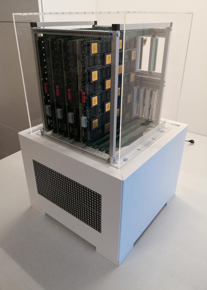
This is it. Hooray! The final Cube as I always wanted it to be.
It just took me about 2 years of planning, blood, sweat & tears, huffing and puffing. Many tries to find the right parts, plenty materials evaluated always trying to keep the budget low.

The sleeping beauty – yeah, it’s a bit snow white coffin’ish

Meet the ancestors

You might have followed the route I took for quite some time now:
It began with the ‘Tower of Power‘, basically a component carrier with a power-supply.
After some years it was replaced by the first Cube.  Well, yes, while it had a somewhat cubic’ish case, is still was just a dull standard industrial case. Not really what I imagined how my computer should look.

Form follows function

If you’ve read some posts here on GeekDot, you might already got the impression that I’m a sucker for design. Well, not that kind of a surprise, given I studied design some decades ago 🙄
I’m also heavily influenced by the works and philosophy of Dieter Rams (mainly for BRAUN) and Hartmut Esslinger (of frog design), of which you might not have heard about, but you know their designs for sure…
So I fell in love with the Parsytec x’plorer and other iconic computer designs like these ‘cubistic’ examples:

Yes, I am a strong believer that a computer, while basically being a rather boring calculation tool, should look good, timeless and might give you an idea of its innards are actually doing something.
We could probably go on forever, defining how a well designed computer should look like. But like the Romans used to say: “non potest argui per gustum” (You can’t argue about taste)…
Let’s say, I’m probably not totally off, given that most designs I like are also on display at the Museum Of Modern Art 😉

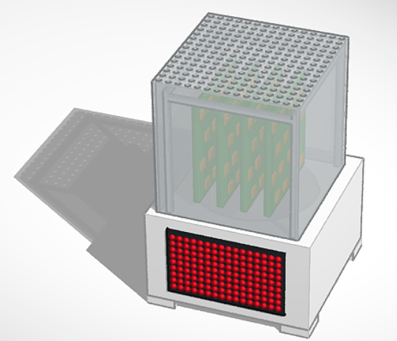
So mentioning the Final Cubes design, it’s  case we’re talking about: If you’re really picky, then yes, the Final Cube is actually two cubes:

The carrier-cage on the top which I tried to keep simplistic and invisible to give the PCBs as much stage as possible. The user should be able to see the many, shining CPUs. So 10x10mm aluminum square tubes are connected by 3D-printed frame-corners to provide maximum view onto the technology.
For protection but also as a design statement and tribute to Rams’/Gugelots famous ‘snow white’s coffin‘ everything is surrounded by a 30x30x30cm translucent acrylic cube.

The white base actually isn’t cubical at all being much wider than tall. Nevertheless, its design should be even more simplistic and cautious to serve three purposes:

  • Give the computing-parts above it a proper podium
  • House the LED array which provides the fitting aura
  • …and finally house all the tech the user should not care about

With quite a big fan between the base and the top both work like a chimney (following the convection) sucking the air from the bottom and blowing it through 169 holes in the top plate of the cube.
Here’s an idea out how it looks “working”:

When one thing comes to another

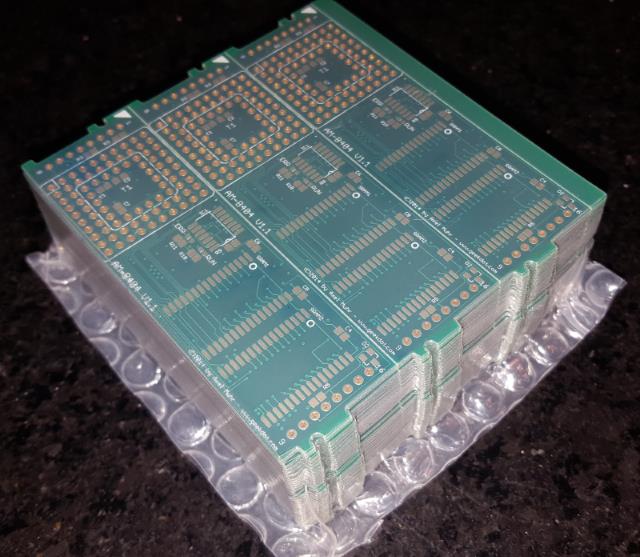
The parts of which the Final Cube is build from aren’t all created this year. Actually only the case and the cage-frame are from 2019 – all other parts were designed by me some years before.

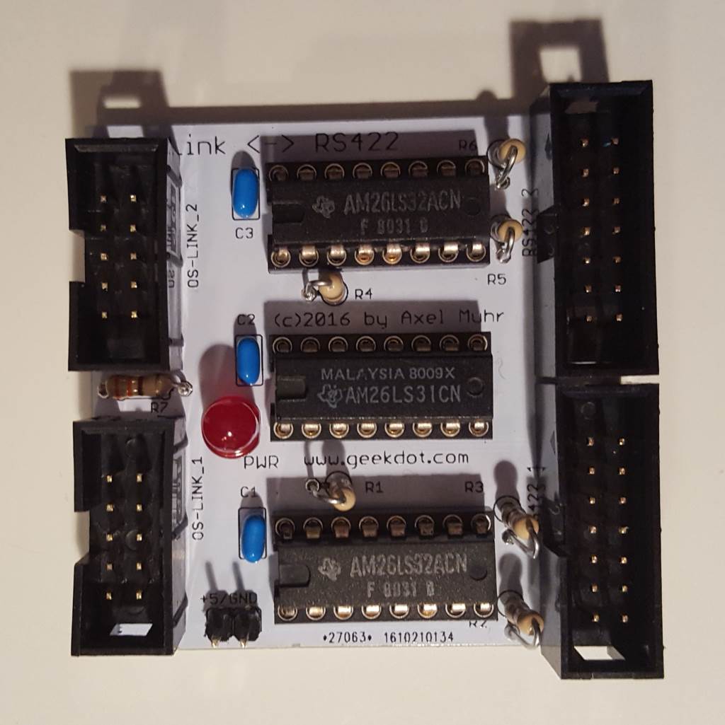
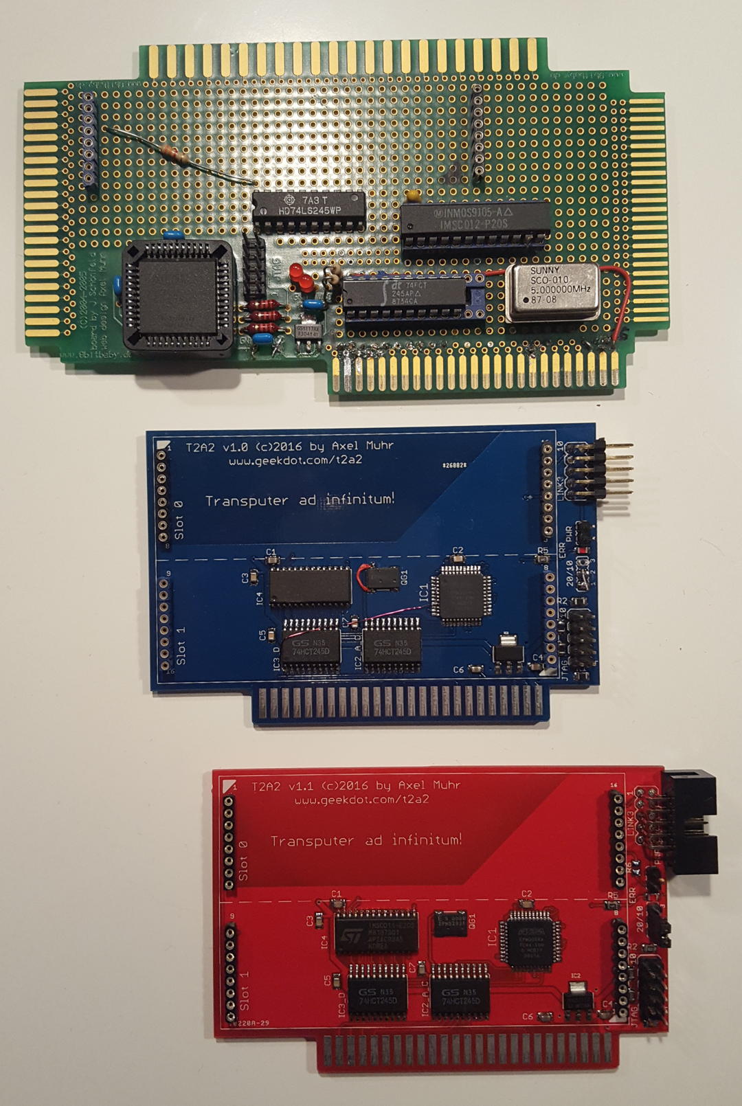
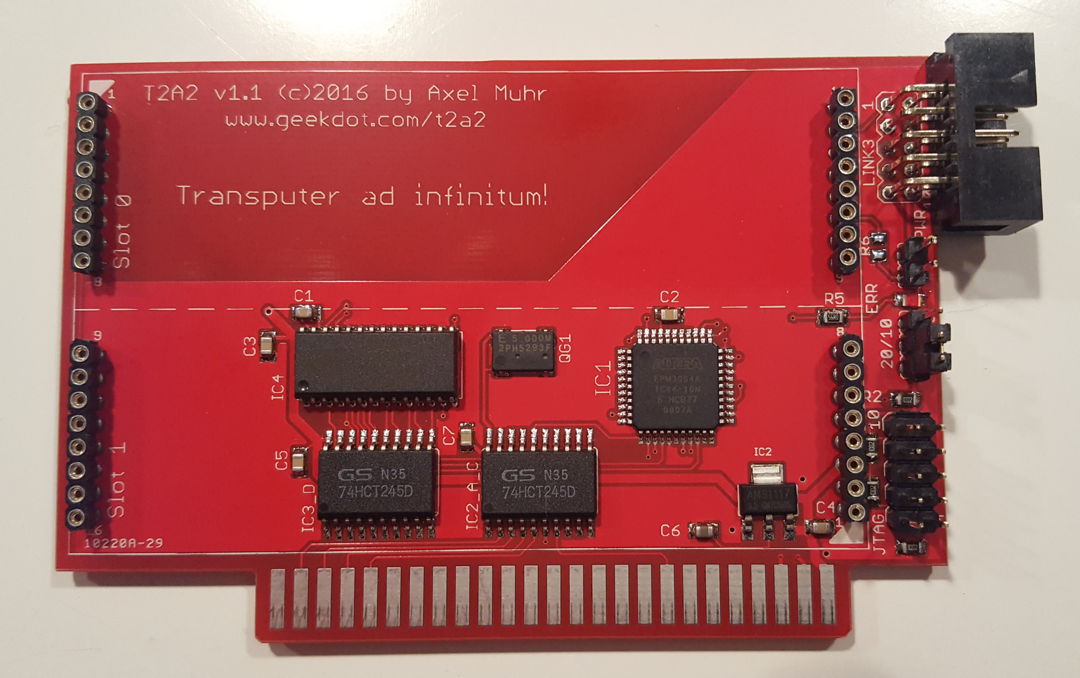
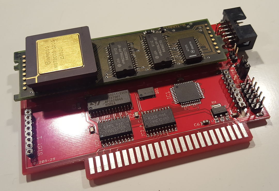
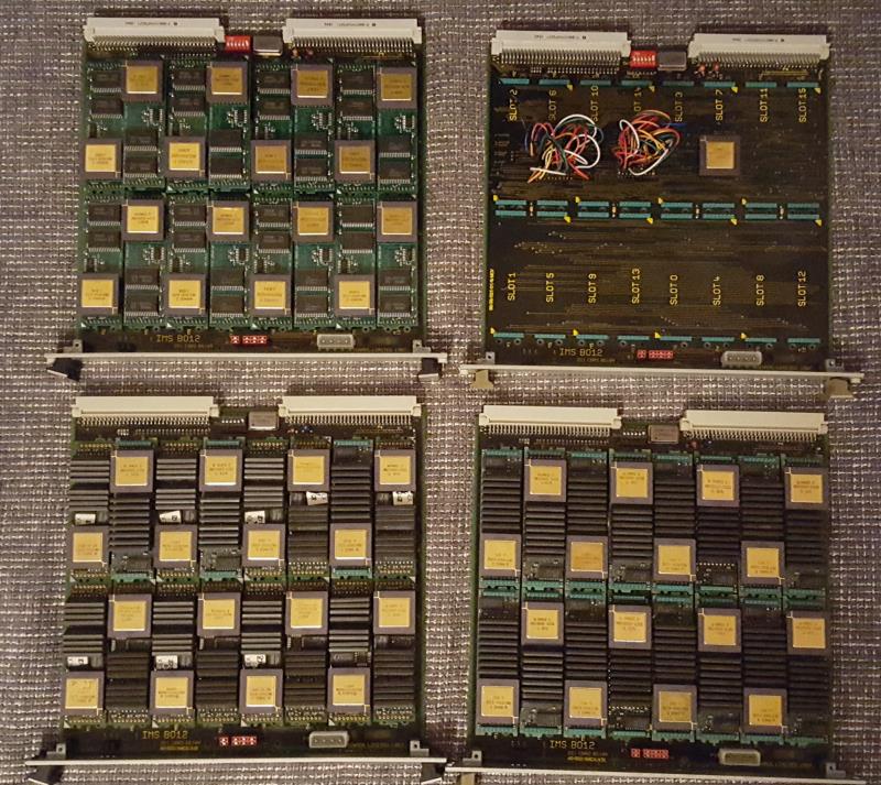
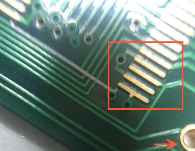
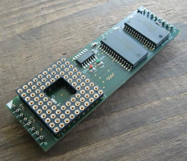
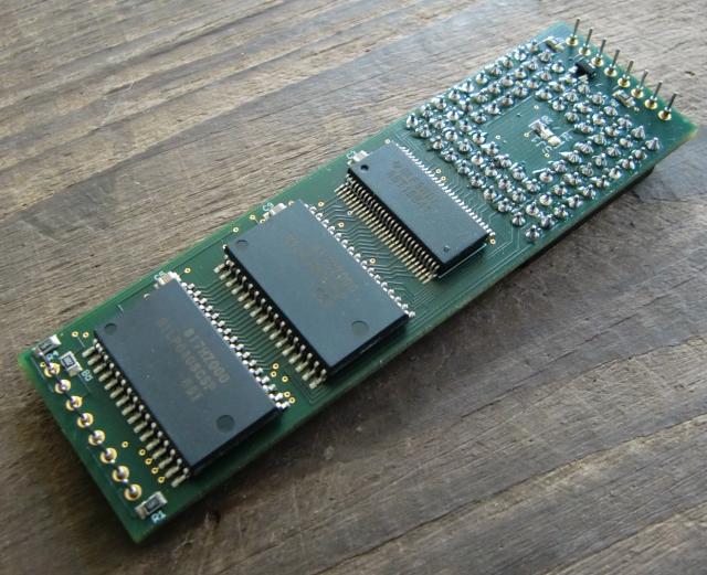
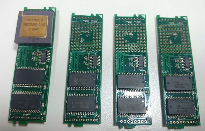
The core of everything are TRAMs – these are Transputer computing modules defined by Inmos back in 1990. The specific TRAMs used are my own AM-B404, each containing a 25MHz T800 and 2MB of  fast SRAM.

Finest home-made TRAMs

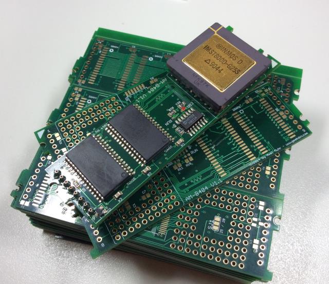
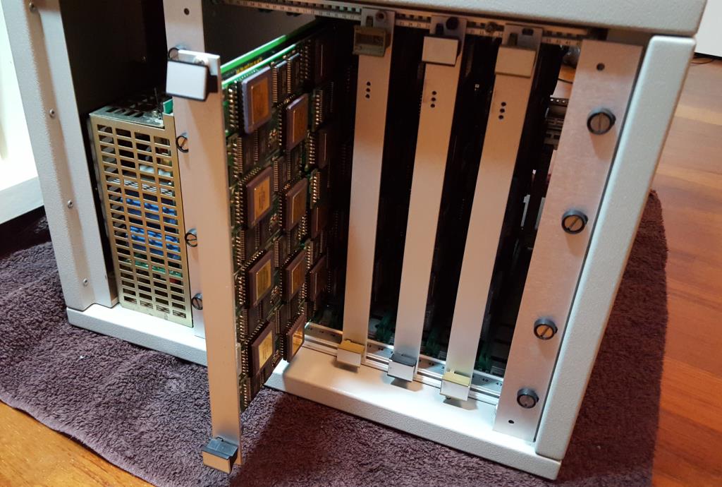
16 of these TRAMs are placed onto an Inmos B012 (or compatible) carrier board. And up to 10 of these carriers can be put into the Cubes carrier-frame creating the cluster.

Under the hood

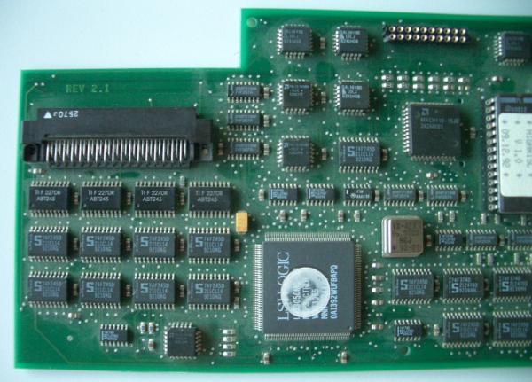
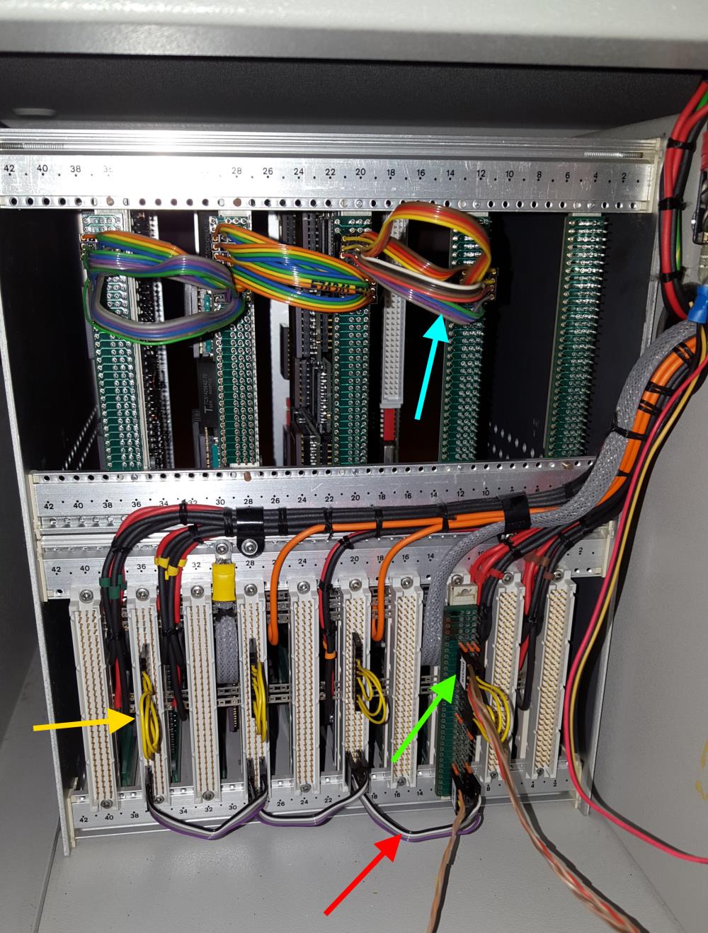
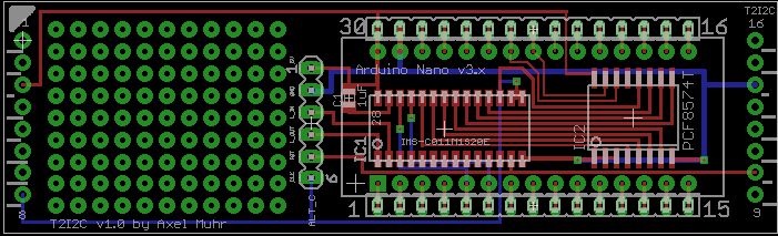
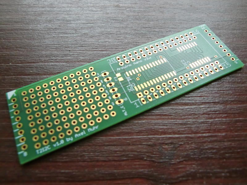
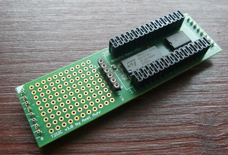
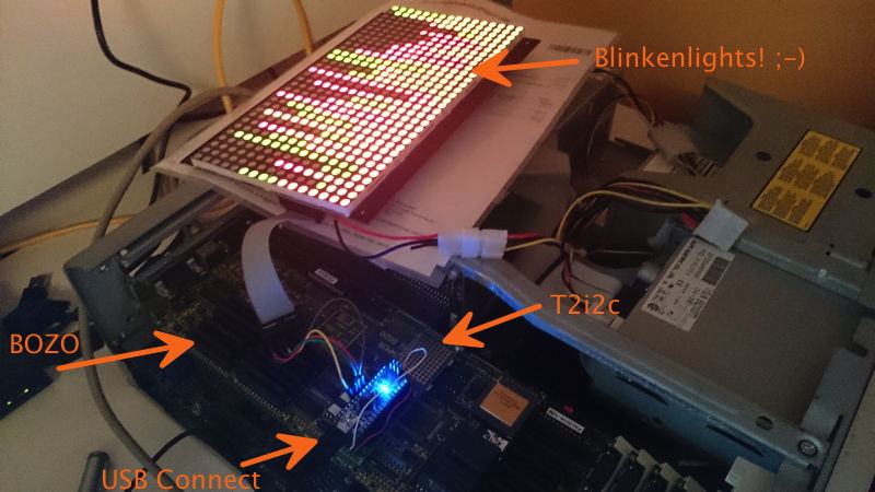
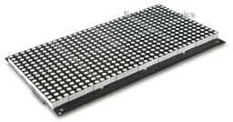
Below the carrier-frame, in the base, you can spot a 32×16 LED panel. This one is actually from 2012 when I designed the T2i2c, an i2c-bus to Transputer TRAM.

Yes, that’s an Arduino Micro on top of a TRAM

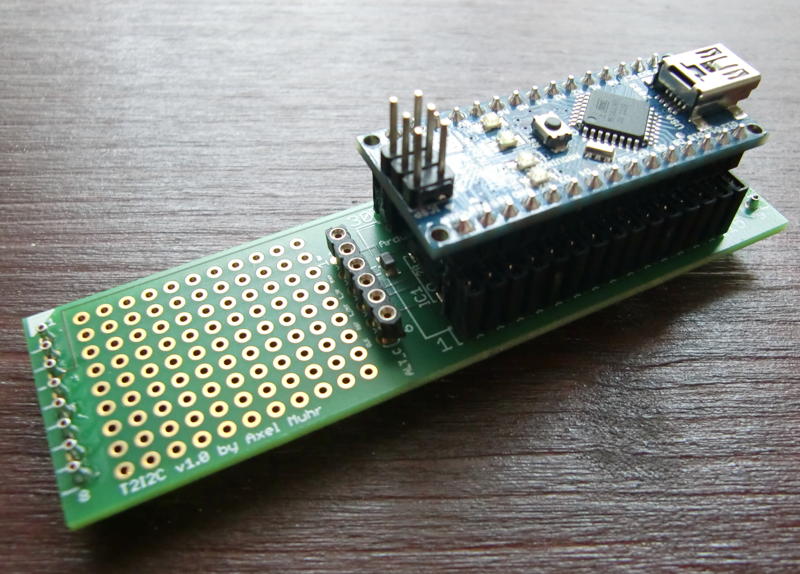
So it was a natural move to make the T2i2c into a system-controller. It does not only controls the LEDs displaying the current load of all Transputers, but also using a photo-diode to set the display brightness as well as measuring the internal temperature and overall power consumption.

Here’s an overview of the base internals:

I know, the venting holes are not pretty – but they do their job and prevent you from accidentally touching the power-supply.

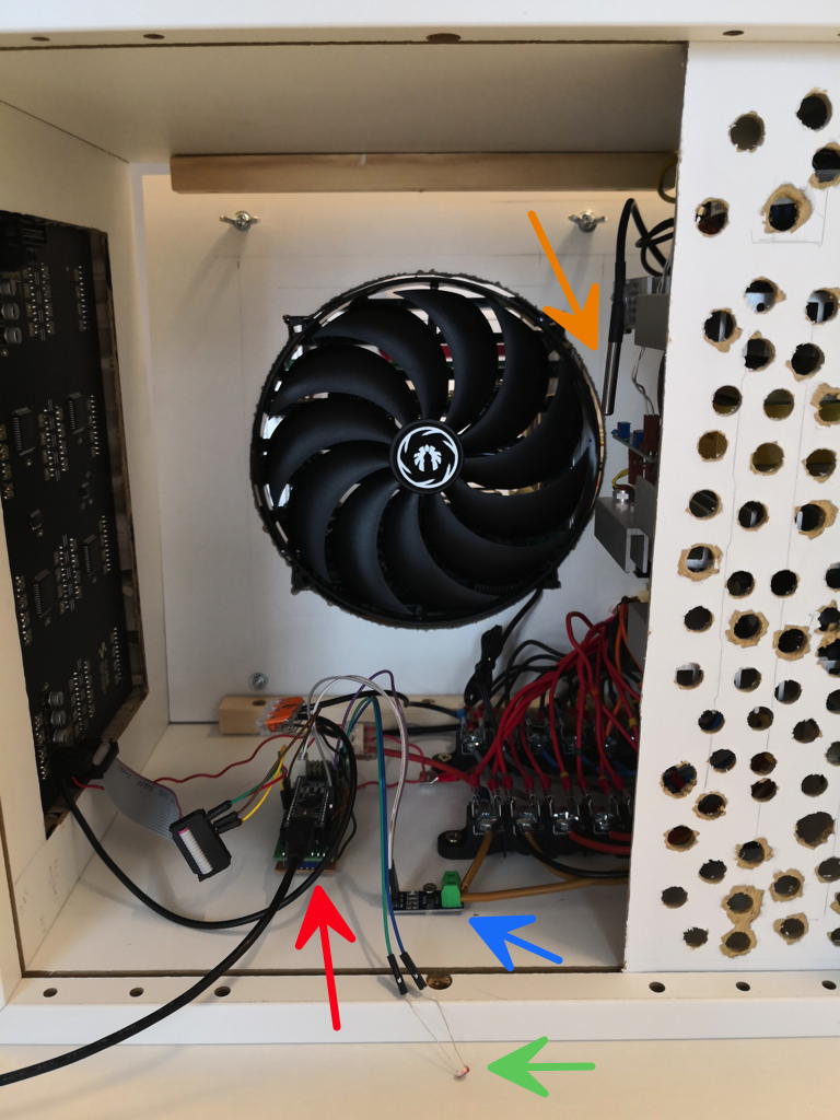
The red arrow points to the T2i2c being connected to the LED panel to the left as well as to a hall-sensor (blue arrow) measuring the power consumption, a temperature sensor (orange) and a photo-diode (green).
You cannot overlook the 22cm fan in the back sucking air from the bottom along the power-supply and pushing it up to the Transputers above to keep them cool.

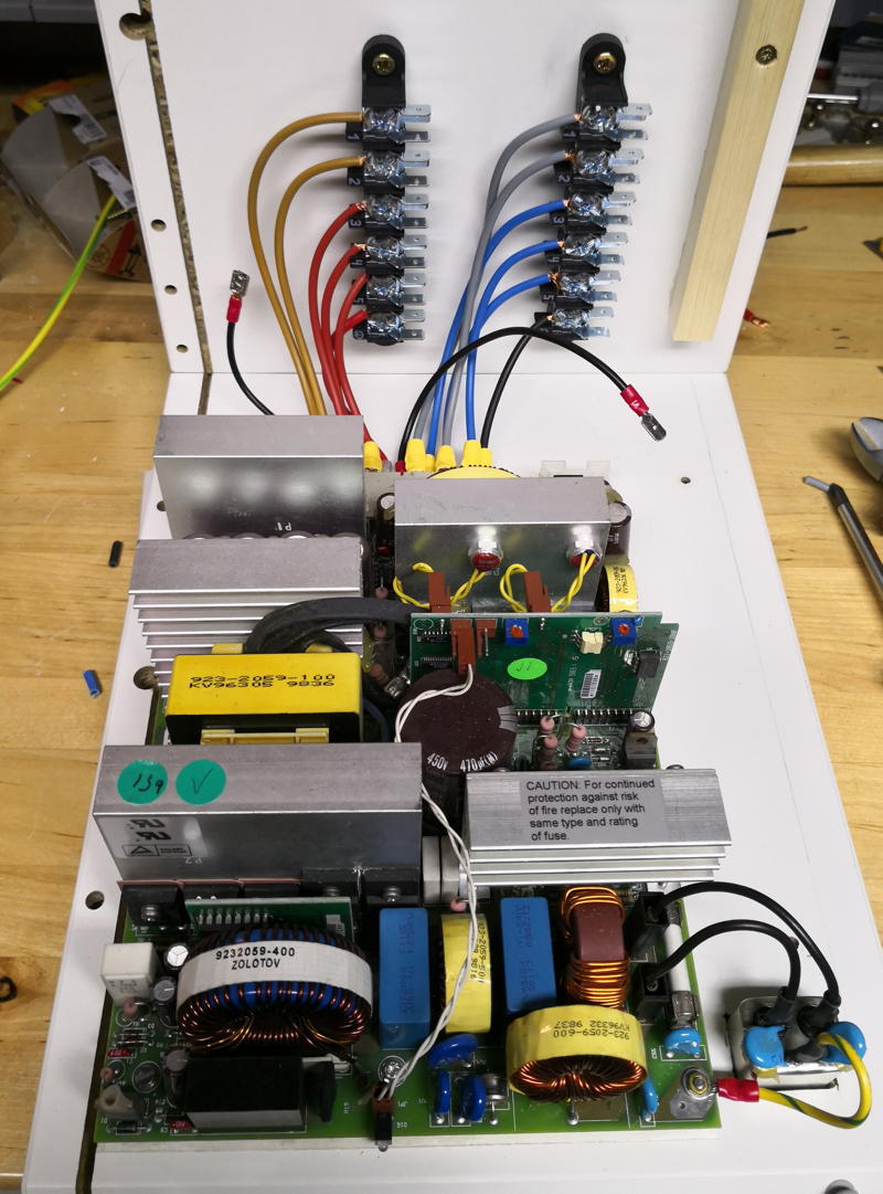
And their power consumption is not to be trivialized. In average a single Transputer TRAM requires is about 1 ampere… so the math is easy. This means the quest for a powerful power-supply was on.
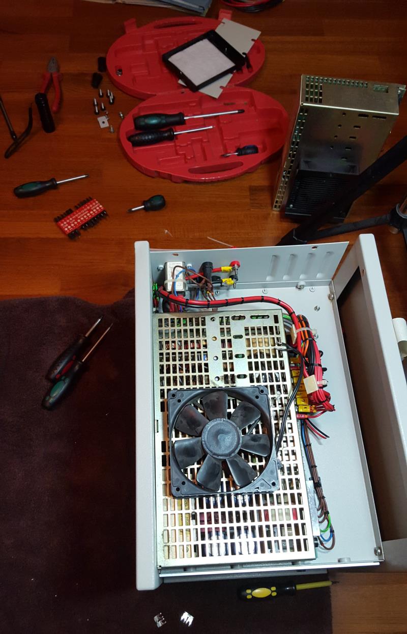
After some months I found what used to be the power-supply meant for a 3Com Corebuilder 7000: The mighty 3C37010A. A whopping 90A@5V should be OK for starters… here’s the fitting procedure:

Mooooore powerrrrrrr, Igor! You touch, you die!

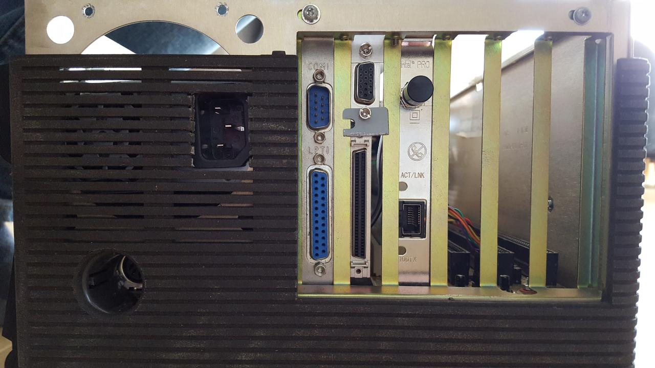
The back of the medal…

The backside did not change compared to the previous Cube back  – well besides the supply-cabling which now goes down into the base instead to the side of the cage.


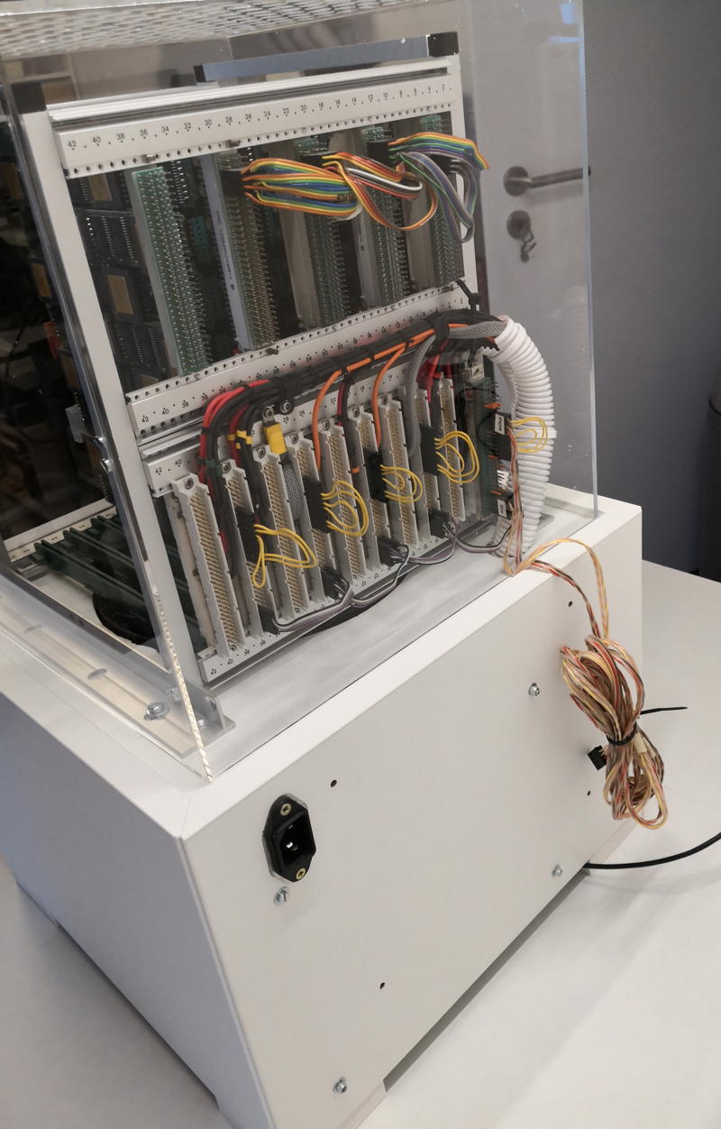
In consequence you’ll spot the power-connector there. No switch though  – still thinking about that… as well as a nicer cable-management for the link-cable which is normally connected to the host.

Next up would be a host matching the look. Mhhhh….

Henkelmann

May I introduce you to Henkelmann – a heavily modded Dolch PAC 486 “portable computer”.
‘Henkelmann’ is post-war German miner jargon for a lunch pail – today it is still often used for “anything big with a handle”… and for todays MacBook Air standards the Dolch is quite big. Back in 1998 is was a 32-bit power house…

In 2008 I wanted a system with full-size ISA slots (mind Transputer or i860 cards) but a bit speedier than a 25MHz 80486, more flexible and silent (as with some others of my systems) I had to change some bits and pieces. Well, in the end nearly everything was modified. In short:

  • Swapped the tiny 10″ 640×480 for an 12″ 800×600 display
  • …which required a new display controller – PCI only
  • …which required a new motherboard
  • …which made larger IDE drives, CD-ROM and USB possible
  • …which required internal space and connectors
  • all of which required proper cooling or something more power efficient.

Before I go into details, let’s have a quick glimpse: From the front, it still looks pretty original (besides the glossy screen):

The screen

Well, from the moment I’ve opened the ‘box’ by removing the keyboard from the front it became clear that I have to change the small 10″ display which was just OK with its 640×480 resolution to be used with DOS but using Windows was out of question. The original system used an ISA graphics card to control the TFT display – these cards are mostly dedicated to a specific kind of display. So both had to go… and I was able to find a new combo at ePay. Being more modern, the new controller card was a PCI card. But that was totally fine as I was going to change the main-board anyways.

As the new screen was somewhat higher than the old one I had to do some sawing and cutting – so most of the side-panels were removed and luckily the hight perfectly fits between the upper and lower outer-edge, so just about 5mm of the very thick plastic had to be cut out there. The cut edges turned white, so I had to do some (bad) paint job, too. It’s not as bad looking in real than it looks in these pictures:

Bottom edge:

One downside is the fact, that the cables and electronics of the display made it necessary to mount it upside-down – technically that’s no issue as there’s a solder-jumper on the graphics-card to make it flipping the picture. The bad thing is, that the display has an optimized view-angle for just the other way round  🙁 So looking from top at a steep angle the picture looks inverted – from a frontal view there’s no difference, though.

Mainboard

As I wanted the best of both worlds, I needed a baby-AT format for being able to re-use the original case openings (AT-keyboard plug!) but also having as many ‘modern features’ as possible, e.g. PCI, IDE, USB, etc.
Luckily I’ve found the DFI K6BV3+/66 which is a Supersocket-7 board in Baby-AT format… how cool is that?!

Because it’s a Super-Socket 7 board I hunted for the best CPU available for that socket, the AMD K6-III+, a real beast for its time – which I planned to underclock to 266MHz, because I wanted to cool it passively. Well not completely… while the K6-III has a low heatsink on his top, there’s no room left for a fan on top of that.
So there’s a small fan on one side of the case (top left corner in the picture below), sucking air in and blowing it over the heat-sink towards the optional ISA cards… not 100% optimal but worked so far.

As the K6BV3+ has just an ATC power-connector a new and preferably smaller power supply had to be found. For that, I had to create a custom mounting using an aluminum angle profile (lower right in the picture below).

The power-button went into the NIC back-panel and a new cutout for the power cable was needed:

Peripherals and Drives

There are just 2 half-height, 5¼” drive slots in the case available. So careful planning was taken to serve every vintage computing need and this is the rather squeezed result:

  • 5¼” & 3½” floppy-drive combo in slot-1 (Yellow & red arrow)
  • Slot-in DVD drive (blue)
  • 2.5″ Harddrive (beneath the DVD, green arrow)
  • 2x USB an 1 PS/2 connector (purple & orange)

Conclusion

All that effort gave me a portable, well, “luggageable” PC which can read and write most media you need for vintage computing. It’s rather fast, nearly silent and most importantly features 2 full-size ISA slots and a shared PCI-slot for more recent stuff.

Digging deeper into the highRISC

After 7 years mainly doing research on Transputers and the i860, I had the feeling it’s time to do some more digging into the highRISC card.
If you have read my initial post about the miroHIGHRISC (and the Tiger) you remember the undocumented 20pin socket on the card (pictured in the upper right corner):

HighRiscLeft

Let’s have another look at the “UART port” again:

The pinout (the connector is rotated 90° counter clock-wise):

GND  oo  /WR0
D0   oo  INT2
D1   oo  /RD
D2   oo  /IOSEL
D3   oo  RESET (most likely)
D4   oo  A2
D5   oo  A3
D6   oo  A4
D7   oo  A5
VCC  oo  A23

Reading a bit of the BIOS’ disassembly, I stumbled across routines to talk to an UART.  A very common (D)UART of those days was the SCN2681. If you take a look at this chips specs, they perfectly fit to the signals provided at the HIGRISCs UART-port!

Here’s its pinout with the corresponding pins marked:


A2-A5 are used for A0-A3 on the 2681 and the only pin not directly represented is A23 which might be used to decode. Also, it nicely reveals that CPU INT2 is used for the UART.

The LR33000 datasheet tells me that there’s an 4MB IO-area starting at 0x1E000000 reaching up to 0x1EFFFFFF- most likely the 2681 will live there… and the corresponding signal called /IOSEL is available on the UART-port (and will perfectly help as chip-select decoder). Tadaa!

So after the UART we need to get the RX/TX signals to a higher level, i.e. the +/-15V of RS232 – this is the call for our old friend MAX232.

[current bread-board experiments sadly didn’t yield into ‘instant success(tm)’… I’m missing out something – need more time to investigate]

Bootcode / BIOS

The LR330xx CPU also has an /EPSEL EPROM select signal, indicating it’s accessing an EPROM expected to start at 0x1F000000 and ends at 0x1FFFFFFF (4MB right below the IO-area).
Using this knowledge and knowing that the MIPS standard boot-vector is at 0x1FC00000, it’s easy to feed the ROM-dump I did some years ago into the disassembler with the correct start address to do his job.

We need to get an understanding of this bootcode first, so that we can get an idea of “what is where” (e.g. ISA bus, UART etc) and later upload our own code and use those addresses.
Just to stick my head a bit into the clouds, the aim is to first port a then common MIPS monitor-program called ‘PMON’ and use that to run some sort of μLinux. But that’s probably another handful of years ahead…
PMON was a good source of information, because it’s originally written by LSI, supporting all the LSI eval-boards. Lo and behold, some of them had a 2681 UART, too… located at 0xBE000000, which is extensively used in my BIOS disassembly  😉
I have a certain feeling that miro borrowed some design ideas from the LSI Pocket Rocket evaluation board (don’t Google it, it’s a mythic being – if you have documentation, mail me!).

So this is the 2681 memory-map then:

#define BASE_2681 0xbe000000
#define SRA_2681 ((1*4)+BASE_2681) // 0xbe000004 status register 
#define THRA_2681 ((3*4)+BASE_2681) // 0xbe00000C Rx/Tx holding register 
#define ACR_2681 ((4*4)+BASE_2681) // 0xbe000010 Aux contrl. register 
#define ISR_2681 ((5*4)+BASE_2681) // 0xbe000014 interrupt state register 
#define CTU_2681 ((6*4)+BASE_2681) // 0xbe000018 Counter timer upper 
#define CTL_2681 ((7*4)+BASE_2681) // 0xbe00001C counter timer lower 
#define START_2681 ((14*4)+BASE_2681) // 0xbe000038 start timer 
#define STOP_2681 ((15*4)+BASE_2681) // 0xbe00003C stoptimer

Using those addresses we should easily identify the comms routines.

Something happens at 0xBE800000 which seems not UART related. So that’s probably the reason why A23 is available on the connector. That way we can ignore access to that address by OR’ing it with /IOSEL to create a /CS.

The DOS side of things

The tool to load a MIPS executable into the HIGHRISC is called DL.EXE. Loading the test-program prints this to the console:

miroHIGHRISC download program. V 1.00
(c) miro Computer Products AG , Germany

CONFIG: I/O-register-address: 0x368 
CONFIG: DRAM - base-address : 0xD000 
CONFIG: DRAM - size : 8 MB
CONFIG: TIGER - RAM - size : 8 MB

Resetcount = 87340

Loading test.zor
text : start=0x80030000 size=0x52c0
data : start=0x800352c0 size=0x520
bss : start=0x800357e0 size=0x150
entry : 0x800301a0
TIGER comm.address : 0x3ffd00
max_used_address : 0x35930 
real_DRAM : 0x800000 
Heapsize : 0x7CA6D0

test.zor sucessfully downloaded.

This gives us valuable information. The DOS-side uses the IO port 0x368 and has a memory window of 16K from  0xD000 to D3FF.
MIPS programs are loaded to 0x80030000 and the 16K seems to be mapped to 0x003FFD00, just 128K below the 4MB boundary of the LR33k address space.

As usual – this is heavily work-in-progress. So this post will be edited while making any new progress. TBC…

RS422 Differential Adapter

This is a Q’n’D but handy design which I was planning for a long time, but you know how things go… A differential adapter is a simple device which translates a single signal/data line in one positive and one negative line, i.e. one is carrying the inverted signal of the other. This is also known as RS422… But why do we need such thing?

Well, differential signals are/were quite common in the world of Transputing to deliver OS-link signals over longer distances (<10m/30ft) or noisy environments and good examples are systems from Parsytec, the AVM-T1, ISA interfaces like the HEMA TA2 or even some custom measure/data-logging solutions.

So to connect to such systems using a non-RS422 (i.e TTL) interface card, e.g. the INMOS B004/008 or the Gerlach-Card you’ll need such an differential adapter.

Technical data

A very simple design on a 5x5cm PCB. All done in trough-hole technology (THT) to keep this a simple DIY project.
It all based around two AM26LS32 receivers and one AM26LS31 transceiver, some resistors and an unavoidable LED  😉

Usage is very simple, too. Just connect the TTL signals to the standard 2×5 shrouded PCB header connector and RS422 signals are provided on the 2×7 header connector on the opposite side of the PCB.
The TTL connector is the same as the one used on the Gerlach card or my T2A2 Apple II interface:

As you can see, pins 9 & 10 can provide 5V to the PCB so that no external power-supply is needed.
If you connect a system not able to provide power to the differential adapter there’s also a 2pin connector provided on the PCB itself.

The RS422-side of the adapter has this pin-layout:

Nice-to-know: You could also use this adapter to simply invert signals. For example if you need a positive ERR signal instead of the not’ed, you simply take the positive pin (i.e. even pin-number 6 in this case) of the 2×7 connector (ignoring the negative).
Mind there’s no power supply pin on that side and pins 11/12 are not connected.

T2A2 for everyone

While the guys over at OpenApple were speculating in their latest podcast what a Transputer actually is… well, there are about a 100 links and ways on this page to find out – but hey… just click here – and of course that box saying search would do great wonders, too.

But seriously, my bad: I should have mentioned that this page your looking at is really just one post of many… so make sure you start at a Chapter (Menu. At the Top. ↑…yes up there) and read them in the order you’d read a book 😉

After quite some years (and a handful Apple II users requests) I felt the urge to finally put the T2A2 prototype (read that post to get a more general understanding) into a real expansion card… and here it is: Say “Hello!” to the T2A2 version 1.1!

It came a long way…

t2a2_evolution

…in more detail:

t2a2_front

As you can see, the final T2A2 is much smaller than the prototype (which used an 8bit Baby one-for-all PCB) and offers many additional features

  • 2 size-1 TRAM slots (or one size-2) – double the processing power!
  • Low-power, low-profile parts used where possible (3.3V CPLD, HCT logic)
  • External Transputer-link available as edge connector – extend your network to “near infinitum
  • Jumpers for LinkSpeed and optional power to the Transputer-link connector
  • Fully buffered to be a good Apple II bus citizen
  • Works in any slot set to “your card”

Beyond this, everything said about the prototype is still true.

Most important:

a) It’s not tested in the ][ or ][+. I simply don’t own one of those.
Update: One owner reported it’s perfectly working in his IIe!
b) The T2A2 won’t instantly speed up any of your Apple II[e/gs] applications.

It’s more like a co-processor attached to it. And even then, you’ll need something really calculation-intensive to justify the time you’ll loose due to communication between the Apple and the Transputer. A single square-root for example wouldn’t make much sense – but having a complex algorithm (like the Mandelbrot fractal in my demo)  does absolutely make sense, as you just pass the parameters to the Transputer and let him do the sweating.

But on the other hand, FPU cards like the Innovative Systems FPE (using an M68881) or my even faster clone “NumberCruncher Reloaded” did just send instruction by instruction. So I somehow fancy the idea writing a SANE driver for GS/OS to integrate the T2A2 more transparently.

Want your own T2A2?

So now you’re keen to get one yourself? Please check this list first:

  • Do you have a TRAM already? (*)
  • You are aware that there’s no real software (yet) besides my little Mandelbrot demo?
  • You are keen to program something yourself – or are fine to wait until somebody else did?

While the Apple II side of coding is pretty easy, you have to get a grip about the Transputer development, too. That includes a DOS/Windows (<=XP) setup and some knowledge of C and/or OCCAM. I’ve created a little Transputer “SDK”, namely a VirtualBox image running DOS.

Plenty of Dev-Docs are available here.  
I suggest using the INMOS cross-compilers for C or OCCAM. An alternative C compiler came from LSC, which might suit you more if you don’t like the INMOS stuff.

Ok, so you’re still with me… so I have the first batch of 20 T2A2 PCBs ready which I will populate on-demand, and for 40€ (plus shipping) one of them can be yours.
(*) I might be able to offer you a TRAM, too. The price depends on available model, RAM size and CPU used.

⇒ drop me a mail tonobody likes SPAM
(Sorry, you have to type that into your mail-client – nobody likes SPAM, so do I)

Also check the T2A2 forum for current availability, shipping procedure and built status.

Some more technical details

Here’s a T2A2 with a size-1 TRAM installed in Slot-0:

t2a2_with_tram

The T2A2’s CPLD programming can be updated any time through a JTAG port (the lower 2×5 pin-row at the edge).
The jumper above it can be used to set the linkspeed for the TRAMs (10 or 20mbps). If you look very close, there’s a tiny LED next to that jumper. It’s the error LED controlled by the CPLD.
The next single jumper enables the VCC pins on the external Link connector, meant for (small!) external extensions. This connector is the same used on the Gerlach card and is very convenient because of its ubiquitous standard 2×5 shrouded pcb header connector. Here’s the pinout:

As said, the V1.1 T2A2 offers two size-1 TRAM slots. Before plugging in 40MIPS of raw processing power consider the amount of juice being pulled there. Depending on the amount of RAM and load a single TRAM can use up to 800mA of power!  😯
Given the max. of 4A on a standard IIgs power-supply, two TRAMs could bring your souped-up GS into trouble… it’s better to use the external connector with just one smaller TRAM or even simply bridge the Link0In/Out pins with Link3In/Out so that the T2A2 works as a TRAM-less adapter.
That said, there are size-2 TRAMs in existence which will snugly fit  and won’t hurt that much.

The Cube

Meet The Cube – this is the Transputer Power-House successor to the Tower of Power, which was a bit of a hacked frame-case and based on somewhat non-standard TRAM carriers with a max. capacity of just 24 size-1 TRAMs…

The Cube hardware

This time I went for something slightly bigger  😎 …A clear bow towards the Parsytec GigaCube within a GigaCluster.
The Cube uses genuine INMOS B012 double-hight Euro-card carriers, giving home to 16 size-1 TRAMs – Parsytec would call this a cluster and so will I.
Currently The Cube uses 4 clusters, making a perfect cube of 4x4x4 Transputers… 64 in total. Wooo-hooo, this seems to be the biggest Transputer network running on this planet (to my knowledge)
If not, there still room left for more  😯

Just to give you a quick preview, this is what ispy responds when ran against the Cube:

Using 150 ispy 3.23 | mtest 3.22  # Part rate Link# [ Link0 Link1 Link2 Link3 ] RAM,cycle  0 T800d-24 276k 0 [ HOST ... ... 1:1 ] 4K,1 1024K,3; Display all 64 lines
1 T800d-25 1.7M 1 [ ... 0:3 2:1 3:0 ] 4K,1 2048K,3; 2 T800d-24 1.8M 1 [ ... 1:2 4:1 5:0 ] 4K,1 2048K,3; 3 T800d-25 1.8M 0 [ 1:3 6:2 5:1 7:0 ] 4K,1 2048K,3; 4 T800d-24 1.8M 1 [ ... 2:2 6:1 8:0 ] 4K,1 2048K,3; 5 T800d-25 1.8M 0 [ 2:3 3:2 8:1 9:0 ] 4K,1 2048K,3; 6 T800d-24 1.8M 2 [ ... 4:2 3:1 10:0 ] 4K,1 2048K,3; 7 T800d-24 1.8M 0 [ 3:3 10:2 9:1 11:0 ] 4K,1 2048K,3; 8 T800d-25 1.8M 0 [ 4:3 5:2 10:1 12:0 ] 4K,1 2048K,3; 9 T800d-25 1.8M 0 [ 5:3 7:2 12:1 13:0 ] 4K,1 2048K,3; 10 T800d-24 1.8M 0 [ 6:3 8:2 7:1 14:0 ] 4K,1 2048K,3; 11 T800d-24 1.8M 0 [ 7:3 14:2 13:1 15:0 ] 4K,1 2048K,3; 12 T800d-25 1.8M 0 [ 8:3 9:2 14:1 16:0 ] 4K,1 2048K,3; 13 T800d-25 1.8M 0 [ 9:3 11:2 16:1 17:0 ] 4K,1 2048K,3; 14 T800d-24 1.8M 0 [ 10:3 12:2 11:1 18:0 ] 4K,1 2048K,3; 15 T800d-25 1.8M 0 [ 11:3 ... 17:1 19:0 ] 4K,1 2048K,3; 16 T800d-24 1.8M 0 [ 12:3 13:2 18:1 20:0 ] 4K,1 2048K,3; 17 T800d-25 1.8M 0 [ 13:3 15:2 20:1 21:0 ] 4K,1 2048K,3; 18 T800d-25 1.8M 0 [ 14:3 16:2 ... 22:0 ] 4K,1 2048K,3; 19 T800d-25 1.8M 0 [ 15:3 22:2 21:1 23:0 ] 4K,1 2048K,3; 20 T800d-25 1.8M 0 [ 16:3 17:2 22:1 24:0 ] 4K,1 2048K,3; 21 T800d-25 1.8M 0 [ 17:3 19:2 24:1 25:0 ] 4K,1 2048K,3; 22 T800d-25 1.8M 0 [ 18:3 20:2 19:1 26:0 ] 4K,1 2048K,3; 23 T800d-25 1.8M 0 [ 19:3 26:2 25:1 27:0 ] 4K,1 2048K,3; 24 T800d-24 1.8M 0 [ 20:3 21:2 26:1 28:0 ] 4K,1 2048K,3; 25 T800d-25 1.8M 0 [ 21:3 23:2 28:1 29:0 ] 4K,1 2048K,3; 26 T800d-25 1.7M 0 [ 22:3 24:2 23:1 30:0 ] 4K,1 2048K,3; 27 T800d-24 1.8M 0 [ 23:3 30:2 29:1 31:0 ] 4K,1 2048K,3; 28 T800d-25 1.8M 0 [ 24:3 25:2 30:1 32:0 ] 4K,1 2048K,3; 29 T800d-25 1.8M 0 [ 25:3 27:2 32:1 33:0 ] 4K,1 2048K,3; 30 T800d-25 1.8M 0 [ 26:3 28:2 27:1 34:0 ] 4K,1 2048K,3; 31 T805d-20 1.7M 0 [ 27:3 ... 33:1 35:0 ] 4K,1 1024K,3; 32 T800d-24 1.8M 0 [ 28:3 29:2 34:1 36:0 ] 4K,1 2048K,3; 33 T800d-20 1.8M 0 [ 29:3 31:2 36:1 37:0 ] 4K,1 1024K,3; 34 T800d-24 1.8M 0 [ 30:3 32:2 ... 38:0 ] 4K,1 2048K,3; 35 T800c-20 1.8M 0 [ 31:3 38:2 37:1 39:0 ] 4K,1 1024K,3; 36 T805d-20 1.7M 0 [ 32:3 33:2 38:1 40:0 ] 4K,1 1024K,3; 37 T800c-20 1.6M 0 [ 33:3 35:2 40:1 41:0 ] 4K,1 1024K,3; 38 T800d-20 1.6M 0 [ 34:3 36:2 35:1 42:0 ] 4K,1 1024K,3; 39 T800d-20 1.7M 0 [ 35:3 42:2 41:1 43:0 ] 4K,1 1024K,3; 40 T800d-20 1.8M 0 [ 36:3 37:2 42:1 44:0 ] 4K,1 1024K,3; 41 T800d-20 1.7M 0 [ 37:3 39:2 44:1 45:0 ] 4K,1 1024K,3; 42 T800d-20 1.8M 0 [ 38:3 40:2 39:1 46:0 ] 4K,1 1024K,3; 43 T800d-20 1.8M 0 [ 39:3 46:2 45:1 47:0 ] 4K,1 1024K,3; 44 T800d-20 1.8M 0 [ 40:3 41:2 46:1 48:0 ] 4K,1 1024K,3; 45 T800d-20 1.8M 0 [ 41:3 43:2 48:1 49:0 ] 4K,1 1024K,3; 46 T800d-20 1.7M 0 [ 42:3 44:2 43:1 50:0 ] 4K,1 1024K,3; 47 T800d-20 1.8M 0 [ 43:3 ... 49:1 51:0 ] 4K,1 1024K,3; 48 T800d-20 1.8M 0 [ 44:3 45:2 50:1 52:0 ] 4K,1 1024K,3; 49 T800d-20 1.6M 0 [ 45:3 47:2 52:1 53:0 ] 4K,1 1024K,3; 50 T800d-20 1.8M 0 [ 46:3 48:2 ... 54:0 ] 4K,1 1024K,3; 51 T800d-20 1.8M 0 [ 47:3 54:2 53:1 55:0 ] 4K,1 1024K,3; 52 T800d-20 1.8M 0 [ 48:3 49:2 54:1 56:0 ] 4K,1 1024K,3; 53 T800d-20 1.8M 0 [ 49:3 51:2 56:1 57:0 ] 4K,1 1024K,3; 54 T800d-20 1.6M 0 [ 50:3 52:2 51:1 58:0 ] 4K,1 1024K,3; 55 T800d-20 1.8M 0 [ 51:3 58:2 57:1 59:0 ] 4K,1 1024K,3; 56 T800d-20 1.7M 0 [ 52:3 53:2 58:1 60:0 ] 4K,1 1024K,3; 57 T800d-20 1.8M 0 [ 53:3 55:2 60:1 61:0 ] 4K,1 1024K,3; 58 T800d-20 1.8M 0 [ 54:3 56:2 55:1 62:0 ] 4K,1 1024K,3; 59 T800d-20 1.8M 0 [ 55:3 ... 61:1 ... ] 4K,1 1024K,3; 60 T800d-20 1.7M 0 [ 56:3 57:2 62:1 63:0 ] 4K,1 1024K,3; 61 T800d-20 1.6M 0 [ 57:3 59:2 63:1 ... ] 4K,1 1024K,3; 62 T800d-20 1.8M 0 [ 58:3 60:2 ... 64:0 ] 4K,1 1024K,3; 63 T800d-20 1.8M 0 [ 60:3 61:2 64:1 ... ] 4K,1 1024K,3; 64 T800d-20 1.7M 0 [ 62:3 63:2 ... ... ] 4K,1 1024K,3;

Here are some more figures:

  • 32 x T800@25Mhz/2MB  (my very own AM-B404 TRAMs)
  • 32 x T800@20MHz/1MB  (mainly TRAMs from MSC and ARADEX)
  • -> 96MB of total RAM
  • -> 70-130 MFLOPS (single precision)
  • ~800MIPS combined integer power
  • ~60Amps @5V needed (That’s 300W  😯 )

So we’re talking about 70-130 MFLOPS here – depending which documentation you trust and what language (OCCAM vs. Fortran) and/or OS you’re using. That was quite a powerhouse back in 1990 (Cray XM-P class!)… and dwarfed by a simple Pentium III some years later 😉
Just for to give you an comparison with recent hardware (Linpack MFlops):

Raspberry Pi Model B+ (700 MHz) ~40 DP Mflops
Raspberry Pi 2 Model B (1000 MHz – one core) ~134 DP Mflops
Raspberry Pi 3 Model B (1200 MHz – one core) ~176 DP Mflops

Short break for contemplation about getting old…

Ok, let’s go on… you want to see it. Here it is – the front, one card/cluster pulled, 3 still in. On the left the mighty ol’ 60A power supply:

Cube_Front_4x

Well, this is the evaluation version in a standard case, i.e. this is meant for testing and improving. I’m planning for a somehow cooler and more stylish case for the final version (read: Blinkenlights etc.).

And here’s the IMHO more interesting view… the backside. It shows the typical INMOS cabling.

CubeBack

As usual, I color coded some of the cables.
The green arrow points to the uplink to the host system to which The Cube is connected to. Red are the daisy-chained Analyse/Reset/Error (ARE) signals. The yellow so-called jumper-cables connect some of the IMSB004 links back into the boards network. And in the upper row (blue) four ‘edge-links’ of each board are connected to its neighbor.

This setup connects four 4×4 matrices (using my C004 dummies as discussed here)  into a big 4×16 matrix. Finally I will ‘wrap’ that matrix into a torus. Yeah, there might be more clever topologies, but for now I’m fine with this.

Building up power

For completeness, here’s a quick look at how things came together.

The 4 carriers/clusters with lots of size-1 TRAMs… upper right one is the C004-dummy test board (now also fully populated). Upper left is pure AM-B404 love <3

ITEM_futter

Fixing/replacing the broken power-supply (in the back), including the somewhat difficult search for a working cooling solution:

ITEM_repairing

The Cube software

Well there isn’t any specific software needed to run The Cube, but it definitely cries out loud for some heavily multi-threaded stuff.

So the first thing has definitely to be a Mandelbrot zoom. As usual, I used my very own version with a high-precision timer, available in my Transputer Toolkit.

Here’s the quick run in real-time – you can still figure out visually each Transputer delivering its result:

Other Transputer and x86 results of this benchmark can be seen in this post over here.

We need (even) more power, Igor!

So this is running fine – using internal RAM only. On the other hand, it seems that the current power supply has some issues with, well, the electric current.
When booting Helios onto all 64/65 Transputers which uses all of the external RAM, very soon some of them do crash or go into a constant reboot-loop.
By just reducing the network definition (i.e. not pulling any Transputers) to 48, Helios boots and runs rock-solid.
Because measuring the voltage during a 64-T boot shows a solid 5.08V on all TRAM-slots it most likely means the power supply either can’t deliver the needed amount of Amps (~60) or produces noise etc.  😥
So this is the next construction site I have to tackle.

To be continued…

Manufacturing PCBs in China?

Ever thought about manufacturing PCBs in China?

If you google this, you most certainly end up with “your mileage my vary”. Indeed it does… and here are my 2 cents:

Because the grass might be greener on the other side of the river, I’ve tested and will keep on testing several PCB houses over the time. So I’ll update this Blog post every now and then… until now, I wrote about

ShenZhen2U

[Oct 2014]
For my AM-B404 TRAM I hadn’t had any other option than have them manufactured in China. 6 Layers and sub-20$ weren’t possible anywhere else. So I tried ShenZhen2U

Ordering

After sending in the Eagle-CAD files their support was great. Several Mails with their engineer (Hi Iver!)  flew back and forth, during which he created a multi-panel board out of my single board design and turned it into a Gerber file and let me having it for a final check before everything went into production.

Quality

Manufacturing and shipping was OKish (20 days in total). At first sight, everything looked great. Nice, professionally framed SMD stencil, PCBs etc were carefully bubble wrapped.
When squeezing the whole stack of PCB it felt a bit ‘bouncy’ – looking at it from the side, it became clear why:

ShenZhenBent

Some PCBs were bent. You can see the gaps between some of them.

Well, when the PCBs were from the 3-part panel separated it wasn’t that obvious anymore. So I started populating them.
This brought me to the next issue. The silkscreen was quite a bit off on some of the PCBs. Luckily, all of them had enough solder pad left to be usable:

ShenZhenMask

In the end, 3 of the 60 boards were completely unusable. They had shorts within the internal layers which couldn’t be fixed even by cutting traces and re-wiring.
I guess all those glitches are the price you have to pay when going “cheapo”.

Update Nov 2015:
I ran a 2nd batch of the same boards from the same Gerber files and mentioned the non-working boards in the 1st order.
This time the quality was very good and they silently added 2 extra boards to my order. Thumbs up, ShenZen2U!

Update March 2017:
I asked for a quote for the same design, same number of boards but their price increased 30% within 15 months – so I had to find another manufacturer capable of doing 6 layers.

Dirt Cheap PCBs

For my QFP-to-BGA adapter – which just uses 2 layers – I tried Dirt Cheap PCBs. I really like the attitude of their site and for just 25 bucks for 10 PCBs it was worth a shot.

Ordering

It’s a no-brainer. Upload your eagleCAD/Gerber file and wait – after some minutes you can even look at a rendering of the top- and bottom layer of your boards. They explicitly state, that this function is beta and yes, 1 of the ~5 times I used their service, that rendering wasn’t totally correct – so don’t wet your pants if this happens. Use a real Gerber viewer instead. That said, you normally have 1-2 days to update your files if I might have found a mistake later.
About 20 days later I got my little brown envelope. Everything’s fine, I’m totally OK with it.
Before using their service, be sure to check their FAQ. You’ll find jewels like this:
The board house will add three tiny numbers to your board: batch ID, a customer number, and our PCB ID. This is so everyone knows which crappy PCBs to send you. Don’t like it? Tough. Buy an entire panel somewhere else.

Update: I also tried their 4 layer service (for which they use an external board house) and while the price is good, the results were so-so.
They did not place the solder-mask on the most fine-pitch part (QFP 100pin) which is a pain in the a** to reflow without getting shorts 🙁

Seeedstudio

A more posh version of manufacturing PCBs in China is Seeedstudio who asked me to check out their “Fusion” service. They even offered me a $30 coupon (thanks!), so why not give it a try?!

Before sending my Gerber files I had a couple of questions and their email service is very good an responsive.
As they offer hard-gold finishing, I thought it might be a good time to create an expansion card with its connectors being plated with hard-gold to make it more robust to plugging the card in and out a couple of 100 times… some mails flew back and forth but in the end they asked for the same price for having the connector-fingers done in hard-gold as having done the whole PCB done in this process (the rest was planned in HASL). That’s 30 vs 230 bucks! Erm, no thanks… not this time.

Ordering

So I ordered some standard 2-layer, HASL finished PCBs, no bells and whistles on Fri. Nov. 25th. Their order form is well designed and shouldn’t leave you with any questions – they even offer a Gerber viewer of your uploaded files, which I think is very cool!
(One hint: When entering your address, the form insists that you enter an EORI tax-number which private persons normally don’t have. A simple dash “-” does the trick, though).
They offer 3 ways of shipping, ~10€ for normal post (10+ days), DHL and FedEx (both 3+ days). I went for DHL – I’m pretty sure “normal post” wasn’t an option for my order when I had the choice. Maybe because of the weight…
Next day the boards went into production.  You’ll be updated about the proceedings by mail – pretty standard today – as well as in you accounts order history on their page.

On Nov. 29th I got an email confirmation, that my PCBs are finished and shipped… and on Dec. 3rd I got the boards in my mailbox. That was blazing fast indeed! 9 days from ordering to receiving

Quality

The cool thing is, that I’ve ordered the predecessor of this design at “Dirt Cheap PCB”, so I have a direct comparison.
Given the simplicity of the design, I haven’t found any glitches or mistakes… the two boards are nearly identical.
If you’re super picky about your design: like Dirt Cheap PCB, Seeed does print some internal ID on your silkscreen – and that’s not in their FAQ.

Conclusion

For a simple design (2-4 layers, no extras) Seeedstudio is comparable to other PCB houses – even a tiny bit more expensive.
Where they shine is when it comes down to support and all those extra features like penalization, V-grooves etc. which the other houses just can’t offer or leave you in the cold when it comes down to getting help.

PCBWIN

So after ShenZen2U became too expensive for my budget (They’re still cheaper than European services) I found PCBWIN being another Chinese manufacturer able to provide 6 Layers for a reasonable price.

Ordering

The order process was very convenient. After  requestin a quote online I’ve been contacted by my ‘personal sales assistant’ (Hi Betty!) straight away.
Their engineers checked my Gerber, clarified some measurements, v-groves etc. which I could explain by sending photographs and drawings. All in all, very a professional and reassuring process during which you also can contact your personal contact by Skype, e.g. if you’re really on a time-pressure.
I can’t give a usual delivery time for this order, as my fell into the  Quingming Festival season, so that added some extra days of delay – but they informed me about this, so all OK here! Including this delay, it took 10 days until shipping. After the usual 20 days wait and some more queuing at the customs office I got this:

Quality

The PCBs and a new stencil were well packed – and a quick visual check (ENIG, masks, printing) was quite satisfying. If there’s anything to critic, maybe the silkscreen printing was a bit  ‘thin’ – but that’s really a minor thing. The first PCB I’ve populated and tested worked fine – so I assume the other 29 will be fine, too 😉

After-sales are great, too. So your personal assistant will stay in touch and is honestly interested in how everything worked out etc.

Conclusion

So as with any other PCB service, it’s the people that make the difference. Yeah, the price is an important item on the list, but as the saying goes: If you buy too cheap, you’ll buy twice.
For me PCBWIN was a win. Thumbs up!

Do you have/had any good/bad experiences with Chinese PCB manufacturers? I’m happy to hear about it in the comments below!

The AM-B404

Here it is, my latest baby, the goal I was aiming for since years (4 to be exact) – not only to get more TRAMs for my systems but also to break the insane price spiral developing in the last years on ePay and other places. >300$ for a TRAM is crazy. Do not pay that amount! Even $100 is too much.

Update: Final version finished! Click here or scroll down for more.
Update 2: You can buy one, if you like…

AMB404-Front-small

My first CPU TRAM called AM-B404 in reminiscence to the IMS-B404 which comes closest to its specs:

  • Size-1 TRAM
  • 2MB low-power SRAM
  • 2 LEDs showing the Transputers status (running and error)

Well, the original Inmos B404 had 2MB DRAM, too (and additional 32k SRAM) but was a Size-2 TRAM and LEDs weren’t available on any Inmos TRAM… and we all know how important LEDs are! 😉 Contrary to the IMS-B404, the AM-B404 is low-profile, SRAM-only, so the whole RAM is accessed at 3-cycles vs. the IMS-B404 4-cycle DRAM.
Using a 6-layer PCB and all-modern SMD parts (well, as modern as 5V parts can get) the power consumption is a bit lower, too. I’d say about 100mA for the whole Board (no Transputer of course). Finally, there’s an easy access solder-bridge on the backside to set the CPU clock (20/25MHz).

AMB404-Back-small

This is just the 1st prototype. After thorough testing, I will optimize its layout a tiny bit and give it the proper shape of a TRAM. When that’s done, we’ll see how I can make you a realistic price offer.

UPDATE:

From Shenzen with love. The final PCB designes arrived and the first test went perfectly fine.

AM-B404stack

And here are the first 4 PCBs waiting to be finished with the Trough-Hole parts (i.e. Transputer Socket and TRAM Pins)… 100 solder-points in total… per TRAM. That’s quite a bit to solder :-/

First4

Video

Finally, here’s a short video showing the prototype AM-B404 in action (running Helios on my Inmos B020). The “exciting” thing is the blinking green LED which shows the CPUs activity. There’s even some brief red LED access (error) during boot-up which is triggered by Helios scanning the Transputer network.
The bright blue LED to the left is the T2i2c TRAM, so all TRAMs on the B020 are built by me now 😉

Want one?

If you hate the greedy ePay prices like I do, drop me a mail. I might have some AM-B404 left… even with T425/T800 Transputers.

Can I have the schematics?

No, not yet. Sorry. I have to break-even on this first…
Since people discovered there’s serious money in the retro-scene, some ‘smart guys’ started to clone every PCB they can get their hands on and thereby steal the initial investment which the original creators made.

I sell them a bit over the price they cost me to produce. And trust me, you won’t be able to go lower than me:
It’s a 6 layer PCB. ENIG Gold.
Sadly SRAM did not get cheaper, really. Especially the (obsolete) 5V 512kx8 I’m using were lately discovered by other projects to be very convenient and so the battle for SRAM was on. If you’re lucky you might get one for 4€… and you need 4 of them.
The 16 pins used to connect the TRAM to its carrier are very special. You have to buy them by the 1000s – 0.15€ a pop… you do the math.

T2I2C – The nitty-gritty details

Ok, so you saw the thing in action and now you want to know more – maybe even build an interface yourself because you’re one of the other ~15 guys on this planet still fooling around with Transputers 😉

Good news! This time I created circuit diagram so you can actually make you own T2I2C – and that’s not enough: I’ve already laid out a TRAM-1 size circuit board using SMD parts of the C011 and 8574 making space for piggy-backing an Arduino Uno on top of that board.

But let’s start with the other details I mentioned the chapter before. I’m totally aware that there are many, many things to improve and optimize – and then there are probably even more I’m not aware of.
Here’s the how and why I did things they way I did:

Oneway

For this first version of T2I2C I’m using an C011 in ‘mode 1’ – that means it is offering actually two 8-bit buses, one for receiving (input, I0-7)) and one for transmitting (output, Q0-7). Because it’s quick and easy I don’t use the I-bus and therefor grounded it.
This means there’s no way for the Arduino to talk to the Transputer side of things. But using an extra bus for input would mean using a second 8574 and obviously using another 4 wires on the ATMega.

The elegant solution to this is using the C011 in ‘mode-2’ – it then behaves like a C012 which means it provides a single butbidirectional 8-bit bus. So why didn’t I used mode-2 in the first-place?
Well, while mode-1 just requires 2 lines for data-control, mode-2 needs 4 lines and some more coding in the ATMega ‘firmware’ e.g. handling the 2 registers provided by a C012 – So yes, I was just lazy and wanted results quick. The next release will certainly use mode-2.

Handshaking

So what is that data-control you’ve mentioned? Using 2 converters (C011/8574) in a row there’s obviously a need for all parties to know when data has arrived and needs to be processed.
The C011 as well as the 8574 provide a pin which flags a “hey, we have something here!” signal (QValid in the C011, /INT in the 8574) . But in contrast to the 8574 the C011 also needs an “Ok, got the data, feel free to fetch the next one” – which is called “QAck”. So the ATMega controls the data-flow talking to the C011 and completely ignores the 8574 which makes it somewhat transparent.
The comms protocol of the C011 can be found in its data-sheet here. It’s all about reading, holding and releasing QValid/QAck in the right timing.

First I was using an external interrupt line on the ATMega connected to QValid because it’s so obvious. But somehow the results were flaky – sometimes the ATMega seemed do choke on some bytes which simply didn’t make it through(*). After some cursing and hair-ripping I decided to switch back to polling – again because I was lazy and wanted to get results 😉
Up to now polling QValid just works great, probably because the ATMega is pretty fast and I2C is pretty slow.
(*) Yes, of course I’ve read all the docs about interrupt-programing and its caveats (short routines, volatile vars etc…) didn’t help.

Achtung! Kommando!

So what is actually going on in the ATMega running “Se Fiiiirmwarrre”? As mentioned in the previous chapter, I decided not to send a complete ‘bitmap’ of 128bytes each time an update occurs. Instead I created a simple command protocol, (currently) consisting of 3 bytes:

  • 1st byte: If < 255 it’s the number of the Transputer data. If 255 (0xFF) command flag set.
  • 2nd byte: If 1st-byte < 255, it’s the CPU-load in percent, else it’s acommand.
  • 3rd byte: If 1st-byte < 255, it’s the Memory-load in percent.

This means a single Transputer information update only takes 3 bytes. A command like “clear the display” is just a single byte.

Of course there are downsides. Updating a complete display of 128 Transputer-loads means sending 384 bytes instead of 128 bytes needed for a bitmap (512 pixels, 2 bits each = 1024bits = 128bytes) – But OTOH you could enhance the firmware for just that case: One command initiates a bitmap-transfer and then you send the 128bytes of data. Mind the could, i.e. this command doesn’t exist yet.

What comes on top of the handling/processing is the calculations needed to be done by the ATMega. There’s a command telling the ATMega how to setup the panel according to columns. If there are less than 33 Transputers to be displayed, each Transputers gets its own line of 16 LEDs. To display 64 Transputers, it will be divided into 2 columns with 8 LED each. 96 Transputers have to get along with 5 LEDs and 128 can only use 4.
No matter how many Transputers have to be displayed, poor ATMega first has to calculate the percentage value into 16, 8, 5 or 4 LEDs, then decide into which column this value goes and finally handle the displaying itself – worst case a 128 times. All this could be circumvent with a bitmap-transfer, offloading all those calculations to the sender (a Transputer in this case). But I’m not sure if this is much cleverer…

The Arduino source (.ino file) is available here. I suggest you have the Arduino Software installed.
There’s still debugging code in the source, putting out info on Arduinos USB/Serial port.

These are the commands currently implemented (in decimal):

001 – 015 : Set display brightness (0..15)
031 – 034 : Set the columns to be displayed (1..4)
099 : Clear the panel display
100 : Toggle CPU-load-only vs. CPU & RAM load mode

Hardware

Like you’ve seen in the video, there’s no real circuit board existing yet there wasn’t a real circuit board around back then. But I’ve created a board layout for a TRAM-1 containing an SMD C011 and 8574 which provides the space needed for a socket to plug in anArduino Nano (the small version of an Arduino Duemilanove) – Version 3.x to be precise. You have to use a V3.0 or higher if you want to use my ‘firmware’ out of the box! This is because the analogue pins (A0-A7) have been rotated in V3.x and up – if you plan to use an earlier version of the Nano, you have to adjust the i2c-pin definition in the firmware source.
Anyhow – Using an Arduino Nano is much more flexible -and cost saving- than putting everything incl. the ATMega on the board itself.
The socket is laid out to be “double-row”, so you can still plug wires right next the Arduinos pins – well, actually this is mandatory at least for connecting to the LED panel.

Currently (v1.0) these pins are used/defined by the firmware on Arduino:

  • Portd: 7, 6, 5 and 4 for connecting the LED panel
  • Analogue input pins 4 & 5 (SDA/SCL) for the I2C bus
  • Portd: Pin 2 connects to QVAL, Pin 3 to QACK on the C011

board

I tried to layout the board in such way that it could also be used as stand-alone, i.e. without being seated into a TRAM slot. Then you would have to provide the Links, 5V, GND, a 5MHz clock and Reset yourself via the alternative connector in the middle of the board, called “ALT_C” . There is still room left which I’ve used for a little breadboard section.

This design is to be considered v1.0 – still things to improve, especially a way to choose the link to be used if the board is actually plugged into a TRAM socket. v1.0 routes LinkIn/Out to the ALT_C socket which needs to be air-wired to the TRAM-pins… not nice but does its job.

If interested, you can download the Eagle CAD files here.

After nearly a year I was able to get a hand full of boards created and populated one using my brand new reflow oven (Reworked pizza oven) and voilá, here’s the T2i2c in flesh, naked:

T2i2c_naked

…a bit more dressed (all parts place)…

T2i2c_dressed

…and finally fully dressed (Nano plugged in):

T2i2c_fullyDressed

So the final question was: Will it actually work? Yes it did! I plugged it into slot 2 of my beloved BOZO, connected the LED panel and adjusted my Helios test-sources a bit, and tadaa:

T2i2c

The cool side-effect of this project is, that you can keep the USB cable connected to your host, while the T2i2c is actually running in a system, giving a perfect  OS-link-sniffer for what’s going on in a Transputer setup.

Also, I reworked my Helios tools for checking the T2I2C functionality. Everthing is now in one single tool, i.e. test-pattern, clearing the panel or manually sending a command. Here’s the source as well as the executableread the source header before using! You can crash your Helios system – you’ve been warned!

Outlook

I won’t say the sky is the limit, but if the T2I2C-TRAM will be full-duplex in the next release (ie. C011 in Mode-2) driving an LED panel would be just one of many other uses this TRAM could fulfill.
Think of all the million things people did with their ATMega/Arduinos: LCD-Displays, SD-Card Interface, Ethernet and then some more. Ok, the speed of I2C will limit that somewhat (I already have made prerequisites in my ‘firmware’ to put I2C into 400kHz/kbps “fast mode”) but still a nice interface for connecting today-tech to your yester-tech.

The T2i2c

Boy, my acronyms are really getting Star Wars’ish now… After the T2C64 and the T2A2, T2I2C sounds like a new protocol-robot but stands for “Transputer to I2C (Bus)”.
The I2C bus is a comparably slow serial bus – even to the Transputers 1990 standards – but in contrast to the Transputer OS-link interface I2C is still alive and kicking… even more since those simple-to-tinker-with controllers like ATMEGA or PIC made there way beneath your soldering gun.

As you might have guessed by now, the I2C bus wasn’t my primary intention to do this interface.
Since I started fooling around with Transputers I was thinking of an LED “CPU load display” like the one the lovely BeBox had… just bigger, a real manly Blinkenlights 😀 It should be at least capable of showing the load of up to 32 Transputers…
So I stumbled across a very nice bi-color 32×16 LED panel (Sure Electronics DP14211 – it seems in 2022 that company was either sold or folded), which is quite easily controllable through one small ATMEGA controller.

LEDPanel

By incident, a friend of mine gave me an surplus Arduino as a present and the decision was made. I’ve build & programmed ATMEL devices before, but Arduino plus breadboard can’t be beaten if you need to get something done quick.

Blinkenlights

It’s quite straightforward to connect the panel (can one say “display”? Nahh.) to the Arduino. To make things even more ‘bus-y’ the ATMEGA talks over just 4 wires to the panel over SPI bus – yet another serial bus, but luckily we don’t have to care about that fact as there’s a library handling this.
So after some days of coding, the “panel firmware” was done. The Arduino is happily talking to the panel over the SPI bus and listening on his I2C bus (another 4 wires) for commands and sends the calculated output to the panel.

Commands? Well, I was thinking about how to handle the data in an efficient manner. The most simple way would have been to have the Transputer sending the complete 32×16 ‘bitmap’. For a bi-color panel (2 bits per pixel) that would have been 1024bits/128bytes each time/interval.
To be more flexible I came up with a 3-byte command structure – for details see the next post.

Old guy speaking new language

So how to connect a Transputer to an IC2 ‘device’? We need two things for that:

  1. The good ol’ C012/11 Link Adapter – turning Transputer links into an 8-bit parallel bus
  2. An 8bit bus-to-I2C converter

We saw the C012/11 in some of my projects already, so piece of cake here. The 2nd converter needed some research and was easily found: A Philips/NXP PCF8574(A). So without control-lines the setup is quite simple:

Transputer → C012 → PCF8574 → Arduino → LED panel

After some hassle with handshaking (see next post “nitty gritty details”) I was able to send bytes to the display using MS-DOS’debug.exe to write bytes to the standard Transputer link IO ports (0x150++, you should know that by now ;-)) using a nice tool called ‘iskip.btl‘ from the INMOS ANSI-C Toolset (also available in my Transputer Toolkit). It simply shortcuts one Transputer link to another, e.g. Link 0 to Link 2. This relieves you from removing your Transputer and put jumper-wires into its socket… very nice and clean solution.

Doing it the right way

Well, while talking to devices through debug is definitely geeky, it’s not what I wanted as a result.
Having more than one Transputer running, watching its CPU and probably RAM load leads to the inevitable target of Helios. At least that’s the No.1 reason I created this interface… but with the command structure of the ‘firmware’ you’re obviously not bound to that OS, e.g. OCCAM programs could control the panel, too.

So the biggest development part was creating a clean way of taking to the panel while running Helios. For debugging and testing I wrote a simple command-line tool which opens a link on the Transputer you have the shell running on, then it sends what ever byte you added as parameter. Fine.
Next was version 2 of that tool, sending 32 fictional CPU-load values (0-100%), version 3 did the same adding RAM-load values.
Then it was time to do it the right way – so I dived into the sources of ‘network‘. network is the Helios tool for examining the Transputer (not IP!) network(s), so it shows the actual load in nice bar charts etc. – pretty much like top does on todays Unices.
While the sources of Helios are available, they seemed to be accumulated from different sources, dumped into an ISO image without caring for symbolic links etc. – in a sentence: They’re a mess.
After some days of try’n’error I was able to compile the sources of network. This made network2 (working name) possible which includes the new parameter ‘led’ followed by the number of the Transputer link to be used, eg. ‘network2 led 2‘ results in displaying the current CPU/RAM load of all Transputers in the network on the panels.
CPU-load is displayed by red LEDs, RAM-load uses green LEDs, overlapping is shown orange. As long as there are up to 32 Transputers each line represents one Transputer (using 16 LEDs). If there are >32 and <65 each line will be split into 2 columns (8 LEDs for each Transputer). This goes on for >64 and <97 (3 columns) and finally 4 columns for up to 128 Transputers – this isn’t very ‘readable’ anymore given there are only 4 LEDs left for one Transputer, but hey! It’s Blinkenlights, who cares!?

So without much further ado, here’s the prototype-beast in action:

For more details, thoughts, outlook and code see the next post.