
As the T9000 had so many new features and architectural differences the “classic” TRAM wasn’t enough to support all that. So INMOS went to enhance the TRAM-model…
And they meant it! Instead of DIL 16 Pins of a “classic” TRAM, HTRAMs could use up to 160(!) pins to communicate to the outside world. Besides the classic 5V, also 3.3V was supplied on one pin as a tribute to the technical progress. Due to the introduction of the DS-Links (vs. OS-Links within the T4xx familiy), each of the four links of the T9000 now required 4 pins per link, resulting in 16 pins for the links alone. Plus many other special links for Events, ConfigUp/Down etc. a minimum of 60 pins were used.
Also each HTRAM now featured a PROM so it could be identified by software.
This is the pinout of an HTRAM extracted from the most recent source (SGS-Thomson B92x HTRAM datasheet, Nov. ’94)
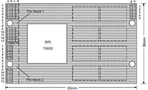
| Pin | Row a | Row b | Row c | Row d | Row g | Row h |
| 1 2 3 4 5 |
ClkIn L0SIn L0DIn L0DOut L0SOut |
N/C GND N/C V3V3 N/C |
TDI V5V0 CupSIn GND CUpDIn |
notTRST L2SOut L2DOut L2DIn L2SIn |
EventIn0 EventIn1 EventIn2 EventIn3 – |
EventOut0 EventOut1 EventOut2 EventOut3 – |
| 9 10 11 12 13 |
L1SIn L1DIn L1DOut L1SOut Reset |
N/C V5V0 N/C GND TMS |
CUpDOut GND CUpSOut V3V3 TCK |
L3SOut L3DOut L3DIn L3SIn V5V0 |
||
| 1 2 3 4 5 |
N/C N/C N/C N/C N/C |
TDO GND CDnSOut V3V3 CDnDOut |
||||
| 9 10 11 12 13 |
N/C N/C N/C N/C N/C |
CDnDIn V5V0 CDnSIn GND N/C |
While many (i.e. 100) pins left unspecified in this pinout-map (e.g. Block 2 rows c & d, Block 3 rows e & f and the complete Block 4), they’re all used on the HTRAMs I own.
My guess is that those were used for the memory-bus, at least in the case of my Quintek board.
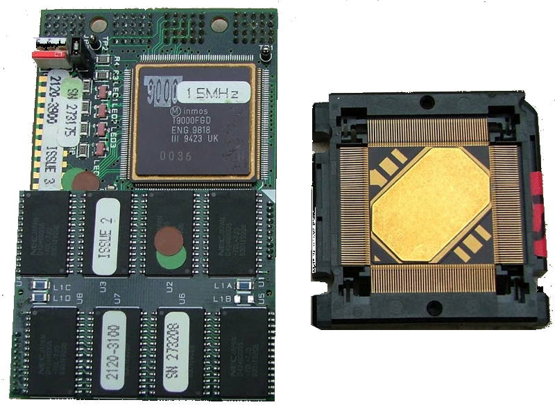
Here’s an original INMOS HTRAM, with a 15MHz T9000 engineering sample mounted, plus a T9000 (backside) next to it:
For a quickstart here are the 3 HTRAMs from Quintek which I own:
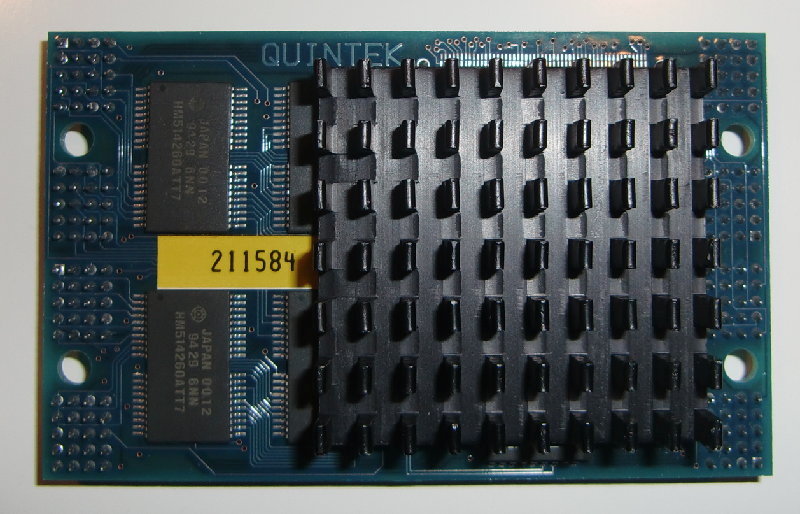
QT9A
The QT9A (Rev.C in this case) is a processor HTRAM of (yet) unknown clock-speed and memory-size – I think it’s 4MB. Because the T9000 ran really hot in the prototype stage (which he never left), all of them required a compariby big heat-sink. I do not dare to remove it, given the (collector) value.
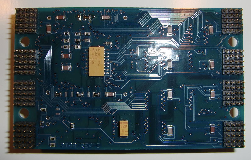
…and the backside for completeness 😉
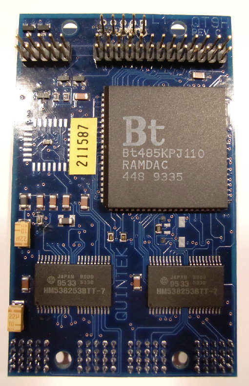
QT9H
This is a display HTRAM featureing a Bt485 RAMDAC, 2MB VRAM but no video-output part. The video signal is delivered to a pin-row which is going connected to a VGA-featurebus on a graphics card. It’s a Rev.C part, like the QT9A.
This and the following HTRAM were fitted into Slots 5 and 5 on the HTRAM-board which are quite special slots: They don’t offer the pin-blocks 1 & 2, i.e. no DS-Links etc.! That said they do feature fully populated pin-blocks 3 & 4 which underlines my assumption that those pins are meant for direct memory-mapping.
In the case of a Video & Encoding HTRAM this makes totally sense because it gives the Transputer even faster access to the Video-RAM than pumping all the data over the Links.
Which leaves yet-another-riddle-to-be-solved: Where are those HTRAM mapped into the T9000s memory?
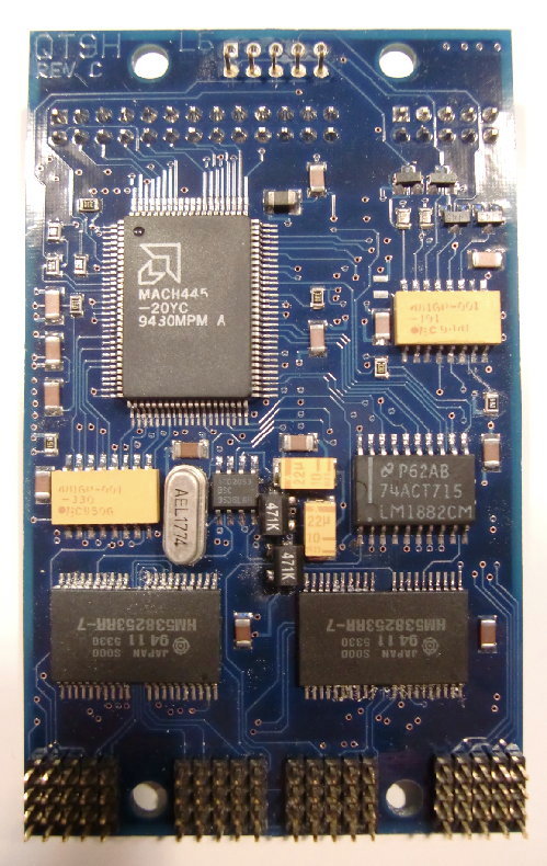
…quite a lot is happening on the back-side, too:
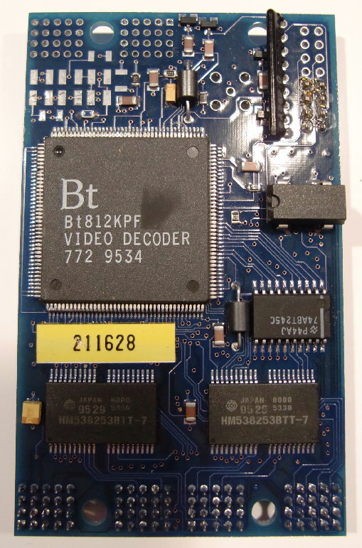
QT9C
A video digitizing HTRAM using the BrookTree/Conexant Bt812 chip and having 2MB VRAM, too… this time “Rev.B”.
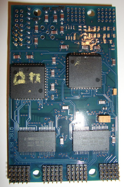
and the back side…
To be continued…