Category Archives: Intel 80860

Intel 80860 Hardware

Microway NumberSmasher

The US company MicroWay (also known for their NDP compiler range), presented an i860 ISA card called NumberSmasher 860.
It was available in two speed grades, costing 11698 DM (@33 MHz) or 14170 DM (@40 MHz). The needed compiler (C, Pascal or Fortran) was an 3135 DM extra.

This 16-bit ISA card featured an 40MHz i860, 4 or 8MB of ram and one INMOS OS-link controlled by a IMSC012 on a litte PCB, hiding 2 additional IMSC012 below it on the main PCB.
It is possible to connect one IMS C012 to to the ISA host bus to “feed” the Number Smasher 860 with programs and data (seedocumentation at the bottom of this page).

Here’s the board in its full beauty:

NumSma860

The left half is occupied by the 8MB RAM. The right half is all bus-logic, buffers and drivers. At the top is a very custom HD-connector – thanks to Jörg Heilmann I now know that this is the FiFo-Connector counting 100 pins. Again thanks to Jörg I also have4 pages of documentation to this connector which was designed to connect the FIFO I/O board (available as ISA and EISA version) to.

On a little separate PCB (having “LINK DR V2.0” printed on it) connected to P3 some sort of additional communication part was placed, consisting of an octal transceiver, one INMOS C012 link-adapter a PAL and an octal buffer featuring two 4-pin connectors (J1 & J2).

  • J1 – GND – GND(code) – to pin 3 of J4 – to pin 3 of J3 – GND
  • J2 – GND – GND(code) – to pin 16 of P3 – to pin 14 of P3 – GND

Additionally there are 3 configuration jumpers – function as far as my measurements go:

  • J3 – Connects pin 18 of the board-connector (LinkIn lower onboard C012) to either LinkOut of the C012 (jumper on upper pin) or to the 4th pin of J1 (jumper on lower pin).
  • J4 – Connects pin 20 of the board-connector (LinkOut lower onboard C012) to either LinkIn of the C012 (jumper on upper pin) or to the 3rd pin of J1 (jumper on lower pin).
  • J5 – Linkspeed for the IMSC012  (upper is 20Mbps, lower is 10Mbps)

NumSma860_Link

Documentation

As I have next to no official documentation about this board I would be very glad to hear from anybody who knows the tiniest bit about this card! AFAIK the original “manual” wasn’t bigger than 13 pages… pretty lame for a board costing as much as a small car back in those days.

Thanks to Jörg Heilmann, I got my first piece of original documentation: The 100 pin FIFO-Connector is described on these four pages. Not much but a start!

Here’s what I found out about the P3 connector on the board, having the “LINK DR” PCB plugged into it. If you have a look at the picture above, I’m start counting pins from bottom right continuing zig-zag like this:

26 oooo...oooo 2
25 oooo...oooo 1

1 – VCC
2 – CLK 5MHz
3 – Reset of the C012 (Pin 11) goes directly to the i860 reset-pin
4 – GND
5 – D7 from ISA Bus
6 – D6 from ISA Bus
7 – D5 from ISA Bus
8 – D4 from ISA Bus
9 – D3 from ISA Bus
10 – D2 from ISA Bus
11 – D1 from ISA Bus
12 – D0 from ISA Bus
13 – ???
14 – Pin 2 of the upper onboard C012
15 – ???
16 – Pin 1 of the upper onboard C012
17 – ISA Pin B8 (NoWS)
18 – Pin 2 of the lower onboard C012
19 – ???
20 – Pin 1 of the lower onboard C012
21 – MEMW to ISA
22 – MEMR to ISA
23 – ???
24 – ???
25 – VCC
26 – GND

From these findings I conclude that J2 is directly connected to the upper onboard C012 while J1 is either connected to the lower onboard C012 (J3 & 4 set to upper pins) or to the C012 on the LINK DR (J3 & 4 set to lower pins) which has its data-lines connected to the ISA bus.

On the main-card are 3 other jumpers:

  • J1 & J2 – Set the connection speed of the two C012 on the card
  • J3 – Select the ISA IRQ. Top down: IRQ 10, 11, 12, 15.

Everything else I have for now is a single article from the German computer magazine “c’t” (3/91,p.164 by O. Grau and A. Stiller) giving a bit more insight in the way the card works:

“Das Interface zum ISA-Bus des Hostrechners ist auf einer kleinen austauschbaren Platine untergebracht und basiert auf einem FIFO. Durch ihn geht sämtlicher I/O. Ein vergleichsweise aufwendiges Protokoll sorgt für einen recht langsamen Datentransfer, so besteht jeder Transfer aus dem Kennbyte 0 (Schreiben) oder 1 (Lesen), gefolgt von der Zieladresse (vier Bytes) und dem Datum (vier Bytes).”

The interface to the hosts ISA-bus is located on a small changeable board and is based on a FIFO [buffer]. All I/O is going through this. A comparably complex protocol is the reason for the data transfer being a bit slow. Each transfer consists of a ID-byte (0=write, 1=read) followed by the target address (four bytes) and the data (four bytes).

This “protocol” sounds very familiar to me. INMOS had the same, calling it PEEK and POKE… I’m still evaluating this, so stay tuned.

[11/05/10] Great News! I had some time and did some deeper investigation… hardware archaeology at its best 😉 So read on in the next post… it’s dissection time!

Hauppauge 4860

Not really an expansion card but a full blown EISA motherboard featuring an i80486 and an i80860 socket directly on board – thus the ingenious name Hauppauge 4860. The i860 can work in parallel to the i486, both sharing the on-board RAM which can be freely partitioned. But theoretically the i860 could also run completely alone… at least Hauppauge mentions this in the manual, announcing a UNIX version for this option (of course that never shipped).

This board is quite a huge beast, full size AT that is. For its time it was regarded as high-quality but besides 1 ASIC and 2 Intel chip set ICs there are a lot of logic ICs and PALs.
I’d say it’s a ‘IC graveyard’ and one of the most exciting 80486 boards ever made.
(And a real diva when it comes to add cards :-/ More on this further down)

FullBoard

These are the main specs:

  • 80486 socket (does not run stable with DX/2), 25 or 33MHz
  • 80860 socket (same clock speed as 486)
  • Weitek 4167 (aka Abacus) mem-mapped FPU socket
  • Intel “485TurboCache Module” socket
  • 7-8 EISA Slots (depending on revision)
  • Intel EISA chip set consisting of 82358-33 EISA Bus Controller and 82357 Integrated System Peripheral
  • On-board Serial/Parallel and PS/2 mouse support
  • 8 SIMM sockets for up to 64MB (Fast Page Mode,parity – No chance with EDO or non-parity)
  • Award “486 Modular BIOS v4.10” / BIOS level 1.01 -obviously specifically tailored to the 486/860 needs.

Because there are so many things on this manly mainboard, I will go into further detail based on quadrants:

Lower right

LowerRight

Well, that’s where all the mojo sits, right. The two processors side by side – ahhh – what a macho view! 😉 Mind the single oscillator: This means both CPUs run at the same speed, which is a bit of a pity, as the i860 was/is available at clock speeds up to 40MHz. Because Intel never really crossed the 33MHz external clock (the 50MHz 486 was quickly replaced by clock doubling versions due to heat issues) for their 486 processor, this is the highest common denominator.
That said, the Hauppauge 4860 does not support DX/2 processors… believe me I tried them all (even up to 5×86 w/ voltage regulator).Yes, it’s running fine one day while failing to boot the next day. So be sporting about it, an AMD 5×86/133 will easily outperform the i860/33 and who would like to put him ashame like this?

Ok, next to the two brains you can easily spot the 8 SIMM slots. It’s not easy to satisfy the RAM specs here: PS/2 SIMMs, optimally 60ns, Fast Page Mode (FPM) with parity – only up to 8MB per SIMM will be addressed. I had to learn that it is not so easy anymore to find those SIMMs today :-/
At the rightmost edge of the board you can see the classic AT-style power connectors… with an additional connector for 5V. Yup, it’s a server board, having all RAM- & EISA-slots populated, this beast can slurp quite some juice. Ok, it still would be nothing compared to todays insane 1000W power supplies feeding quad-core CPUs and dual graphic-cards.

At the lower edge you can spot quite some logic ICs. That’s a part of the memory interface – yeah, no stinkin’ ASIC, just TTL logic and many GALs.

Lower left

LowerLeft

While or two processors still peeking over the right edge, you can easily spot even 2 more sockets on this board. The square one on the left is meant for a Weitek 4167 (also known as  “Abacus”) while the two pin-rows in the middle of the picture are planned for an “Intel 485TurboCache” (yes, that’s 485) module.
Honestly, I have no idea why Hauppauge added the Weitek 4167. As it was just about a bit faster than the inbuilt FPU of the 486/33 (~10% overall), it had no chance against the i860 – both needed programs which were specifically made for them, so compatibility wasn’t an argument for both. I guess it was added on the board just because they could… which is the right spirit!
The socket for the “485 TurboCache” was a good idea – which seems to went wrong in the case of this board. The module generally is nothing more than an i82485 cache controller with 64 or 128k SRAM. After years of searching I found two different models, both not working with the 4860. This seems to be a known issue to Hauppauge as you can find complaints in old (’92) newsgroup posts and Hauppauge itself suggesting not using this module.

Upper left

UpperLeft

This is the most modern part of the board (as by 1992 standards). It’s actually using ASCIs and not only 80’s-style PLDs. In the top-left corner you’ll spot the Samsung 82C452, which is controlling the 2 serial and 1 parallel port(s) on the board.
Next to it is all the Keyboard/BIOS stuff – one fine thing to mention: Hauppauge used an external battery for the settings/clock. Thanks to god they didn’t use some of those nasty Dallas SRAM/Clock chips. After 10 years the internal battery get weak and there’s no way the replace just that (well, there are ways, but that’s really the last resort).
Now it’s getting serious: ASICs, made by Intel… a chip set! Woohoo! Namely the 82350 Intel chip set (Click here for a lenghty article I wrote about this chip set).
This chip set comprises the 82358-33 EISA Bus Controller (EBC) and the 82357 Integrated System Peripheral (ISP). Together these two devices implement a functional interface to the EISA bus,  and provide most of the standard peripheral functions necessary to implement a minimum EISA solution. In a simple sentence: The EISA interface.
That said, there’s a catch: The 4860 being an early EISA board, does not feature the more ‘modern’ 82358DT EBC you’ll find on most EISA boards. This might be the reason why some EISA cards refrain from working with this board. I found a snippet saying “The 82358DT is a superset of the original 82358 and includes a mode compatible with the 82359 Buffered Bus“. The 82359 DRAM controller is obviously missing (probably not a available at that time) and the RAM controller is implemented in lots’o’GALs.

Across the bottom of the picture there’s another slot, looking a bit like EISA… but it’s not! That’s the Hauppauge 64bit Framebuffer Expansion Bus. Hauppauge sold a graphics card basically containing 4MB of VRAM which could be directly accessed by the i860 at very high speed. That made the board a graphics-accelerator like for example the SPEA Fire.

Not much is known about this framebuffer card. Still, I was able to find a blurry press photograph in an 1992 computer magazine. Obviously it’s mainly buffers, GALs, VRAM and 3 RAMDACs for R, G and B… I do have an AutoCAD ADI driver, but I guess you won’t get this board anywhere on the planet anymore 🙁

4860-Framebuffer

Here’s a better photograph I just dragged out of the web:

4860_vidcard

Upper right

UpperRight

Welcome to the end of our tour… the boring part – at least at the first look. 8 EISA slots and some buffers. Nothing exciting, really.
If you take a close look, you’ll see the sticker between slot 6 & 7 (counting from the bottom). This sticker tells you that this board is a “rev D2”:

RevDetail

I don’t have that much documents to figure out the tiny little differences to older versions, but the big one is slot #2. In previous revisions, that slot was ISA… a heritage to this fact is, that on REV D2, this slot is a “non EISA bus master slot” – which is also true for slot #7 (inline with the Frambuffer-Card slot).
The reason for this is (my assumption, though) that the 82357 (ISP) integrates seven 32-bit DMA channels, of which 6 routed to the EISA slots and one used for the Framebuffer.

That’s it for now. I will add new findings as I proceed with my fiddlings.
Thanks for joining the tour, don’t forget to buy a T-shirt in the merchandise shop at the exit…

Software

For the whole enchilada, get the 4860 Manual here. That’s real men reading stuff… i860 source code samples included.

This is the official tools and driver disk and here’s a (yet) small archive containing the ADI drivers for the Framebuffer card and the i860 APX specifically tailored to the Hauppauge 4860 (i.e. won’t run on any other i860 system).

Another nice find: The presentation held at Hot Chips Conference 1990. It gives some more insight into the board design and ideas behind it.

Nostalgia

I found a short article in one of my old (German) computer magazines (“MC”, 1992). Here it is for your amusement/riddling:

The SPEA cards

Between 1990 and 1995 the German multimedia-card manufacturer SPEA was one of the leading companies in this sector (When ATI was comparably small and NVIDIA not even founded).
They offered a wide range of display-cards, from a simple ET4000 up to very expensive CAD/CAM cards using various graphic chips like the TIGA controllers, Hitachi ACRTC, Weitek, S3, 3DLabs and… of course the i860.
Later SPEA was bought by Diamond Multimedia and some employees started their own company to finalize the graphic chip they already started to design when being with SPEA (read more here… article in German, sorry).

Two SPEA cards using the i860 were built. The first was the

SPEA Fire

SPEA-Fire

This full-size ISA card features a 33MHz i860 with 4MB own RAM as well as 2MB VRAM. An Inmos G364 graphics controller is in charge for creating a picture on the monitor – BTW that’s the last and fastest graphics controller which was manufactured by Inmos.
Theoretically, this card could be called an INMOS B020 on steroids.

As this is “just” a 3D subsystem, a standard VGA was still needed for all 2D stuff. Its video signal was then looped-through the SPEA Fire… just like the Voodoo cards did it some years later.

A recent photo I’ve found on ePay shows, that there was a proprietary memory expansion available, which has to be plugged next to the i860. Probably expanding the RAM to 8MB, which can be considered as an quite serious amount of RAM back in those days.

SPEAFire_RAM_upgrade

Interestingly the manual briefly touches the possibility to be programmed with own applications using Intels APX system. Sad enough, the APX is not included on the driver disks and was sold separately for a lot of money.

FGA860

SPEA-FGA860

The FGA860 is the bigger brother of the SPEA Fire. Actually it’s two boards sandwiched together: The one on top is -again- called the Fire-Board. But this time it is designed completely different. There is no RAMDAC or such… just the i860, RAM (16MB) and some custom- and bus-logic.
Behind this, there’s a full-blown TIGA card called FGA-4E, using a TMS34020/32Mhz with 4MB DRAM and 2MB VRAM. Not so usual is the also included VGA part on the FGA-4E. This way you can save an ISA slot for the needed VGA card.

The Fire-Board was available for 5700 German Marks, the FGA-4E added another hefty 10.820 Marks making a total of 16.520 Marks (1990/91 that was about US$ 8000)!
But for that money you got a “graphic subsystem” which was capable of 300.000 2-D vectors/s (10 Pixel long) and amazing 30.000 gouraud-shaded polygons/s (10 × 10 Pixels).
[Back then, that really was amazing… today every mobile phone might be better in 3D. Here are some numbers for comparison/amusement:
3DLabs GLINT 300SX: 500.000/300.000]

Here’s a view from the top… not really much to see. It’s very hard to pry those cards from each other. I guess, they were never intended to be separated again.

SPEA-FGA860_sandwich

If you are in need of the drivers, I make them available here. It’s the IMHO most recent version from August 1994 including an AutoCAD 13 driver update.

Kontron SBC860

First of all: I do not own this card, I just list it for completeness.
Everything written here is accumulated through computer magazine articles or internet sources – if you know more or better, I’m always happy to hear from you.

This is a picture of the Kontron SBC860 (courtesy of Jörg Heilmann):

Kontron_SBC8601

As you can see the SBC860 is much higher integrated as all other i860 cards presented on this page (while it bears quite some similarities with the rev.1.6 of the DSM860-OEM/16), most parts being used in modern SMD form.
It’s a single, full-length 16-bit ISA card, featuring 8 proprietary SIMM slots for up to 32MB RAM.

As far as I can see, the SBC860 has its own bus-interface so no fancy Transputer-Links or such.
In the upper right corner of the card are two huge “pin arrays” (each with 112 pins), the left one having two blue jumpers set. Iassume this could be some sort of expansion-bus for add-ons. Interesting fact: Exactly this part was missing on the board which was reviewed in the German magazine c’t 91/3. As Jörgs card says “R14/A” on one label this might hint towards his card being a later, updated version.

The price of the card was as hefty as their competitors: 33 MHz/8 MByte 13212 DM, 40 MHz/32 MByte at ~21200 DM in the year 1991 (US$ was roughly half)

P3 = Interrupt Vector
7  10  11  12
:   :   :   :

P4 = I/O Base Address   8 consecutive Port Adresses, between 0x100 and 0x3F8

   P4              I/O Addr
==============================
::IIIII            0x300
::II:II :::        0x320
::IIII: :::        0x308
:I::III            0x200 

The DSM-860 Series

Based on a public project from Rolf-Dieter Klein and Tobias Thiel (“PC-Karte mit i860”) in the German computer magazine “mc” (2/90 to 7/90), the Munich based company DSM built several i860 boards for the PC/AT which they called the DSM-860 series.
All DSM-860 have one thing in common: They offer a high level of hardware features – no costs were feared. So naturally, those cards were not cheap. But you really got something for your money. All versions featured

  • 4 Transputerlinks for networking multiple cards
  • Connection to the hosts system-bus (ISA/EISA) via dual-ported RAM
  • A 16-bit bus is also available via dual-ported RAM on special connectors giving a throughput speed of 8MByte/s for high-speed connections between several SPC boards.
  • RAM was put on an extra RAM board making the complete SPC-860 a double-card sandwich

DSM-860

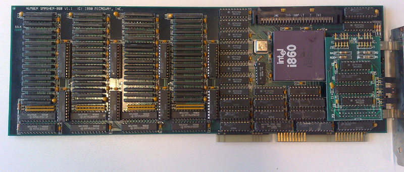
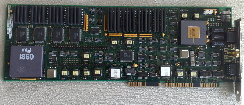
The 1st incarnation was the SPC-860, very quickly renamed to DSM-860, an 8-bit ISA card with 4MB RAM (DIL) and 4 10mbps Transputerlinks via four C012’s (polled by the i860 resulting in 740kbps linkspeed).

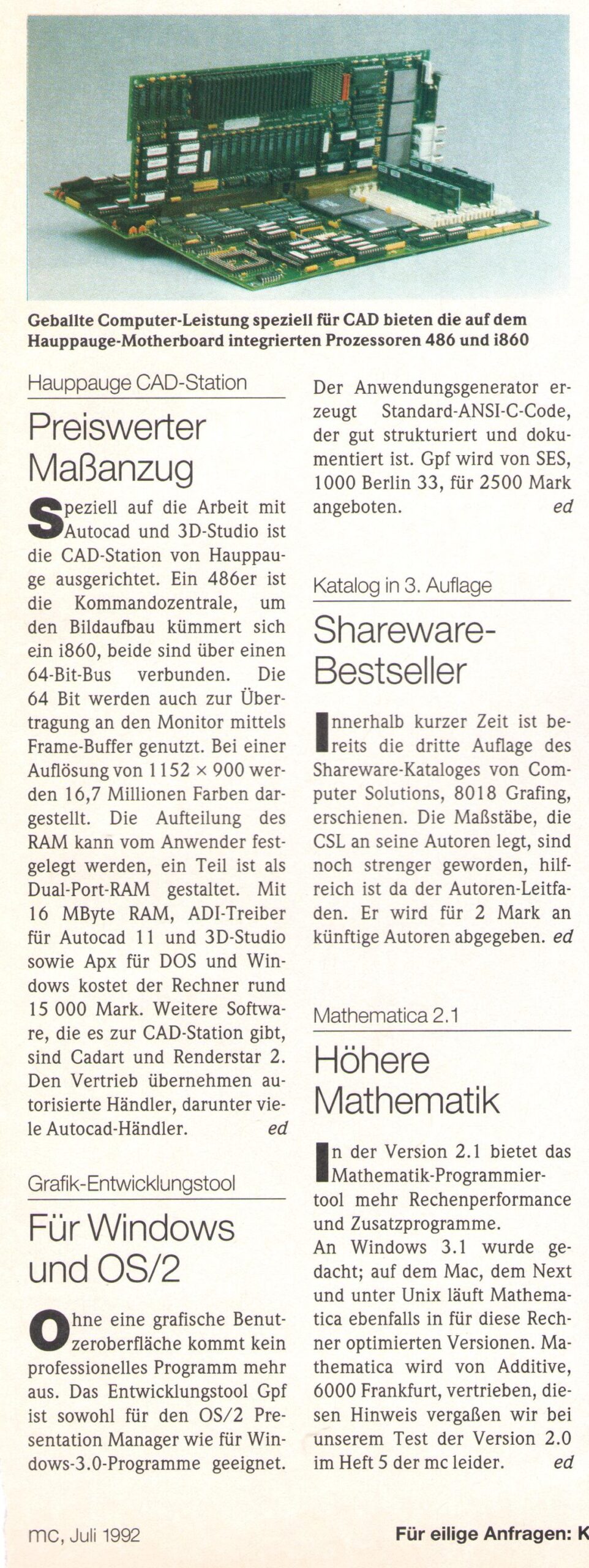
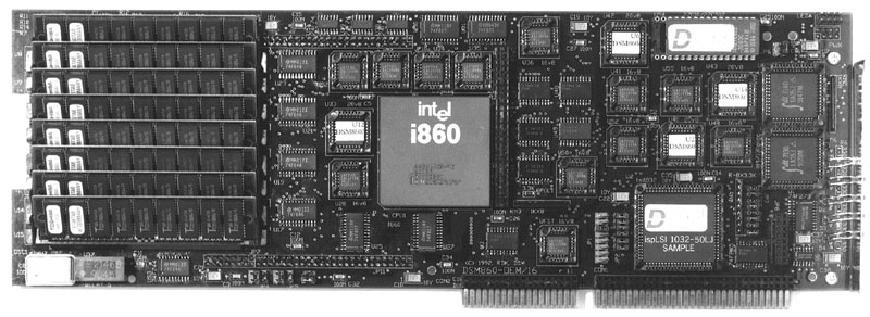
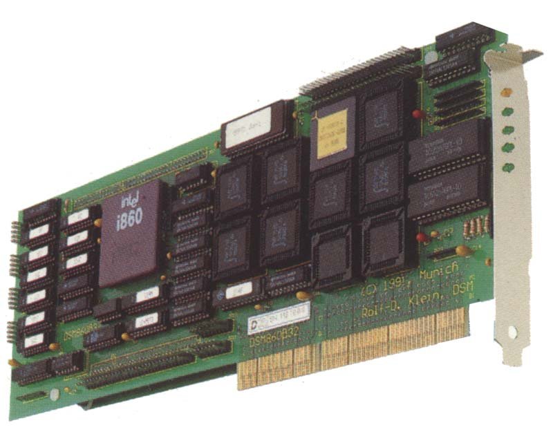
Here’s a picture from a 1992 ad, with separate RAM card attached:

print-DSM860-8

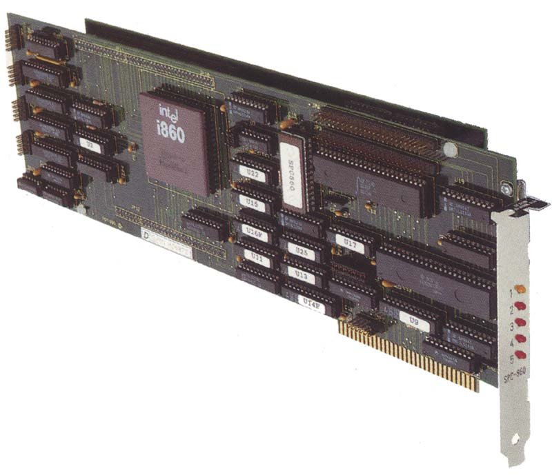
It did cost 16450 DM including the (GNU) C compiler and assembler.

DSM-860/16

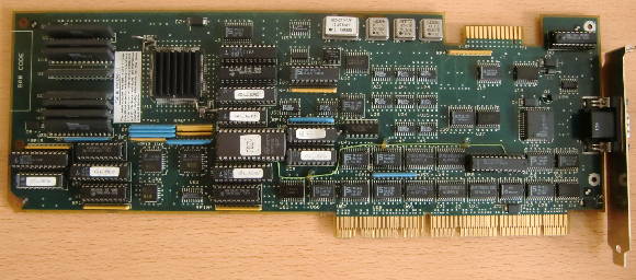
Next, they released the DSM-860/16 (renaming the DSM-860 into DSM-860/8) being a full fledged 16-bit ISA card. It has a real Transputer (16bit T222, having its own 32K SRAM) for handling the “multiprocessor communication” and is able to support up to 256MB on a sandwiched daughter-board, now using SIMM modules instead of DIL parts.
The Hitachi HD63310 dual-ported RAM, used in the 8-bit version to communicate with the host was replaced by faster Cypress IDT7130 types (“because of the high speed of the 16-bit ISA interface” ;-)), resulting in a peak-rate of 14MByte/s.

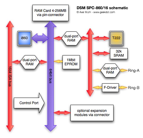
Here’s the schematic of the card and its components

SPC860schem

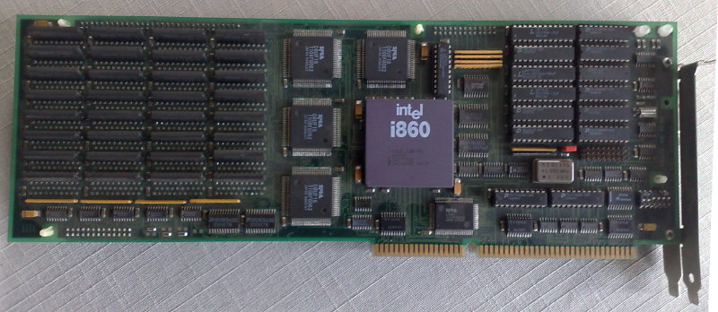
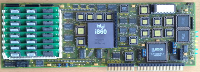
This is how it looks in reality… my DSM-860/16:

DSM860-16

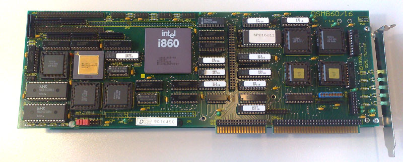
As you can see, the card is not exceptionally high integrated – even built 1992 there is not a single SMD part used, everything is socketed, only some PALs could be called “custom parts”. But this does not necessarily mean it’s badly designed or build.
If you have a close look (click the picture for a bigger version), you’ll see that every part/socket/jumper on the board is nicely specified in the silk-screen printing. All GALs and the EPROM contents are available in the documentation… which has 426 pages by the way.

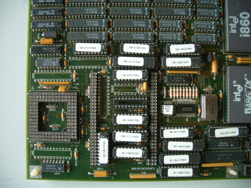
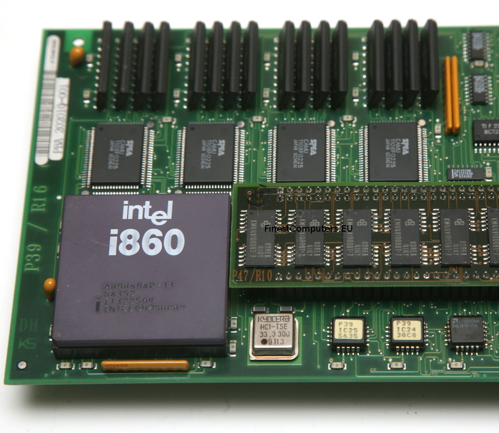
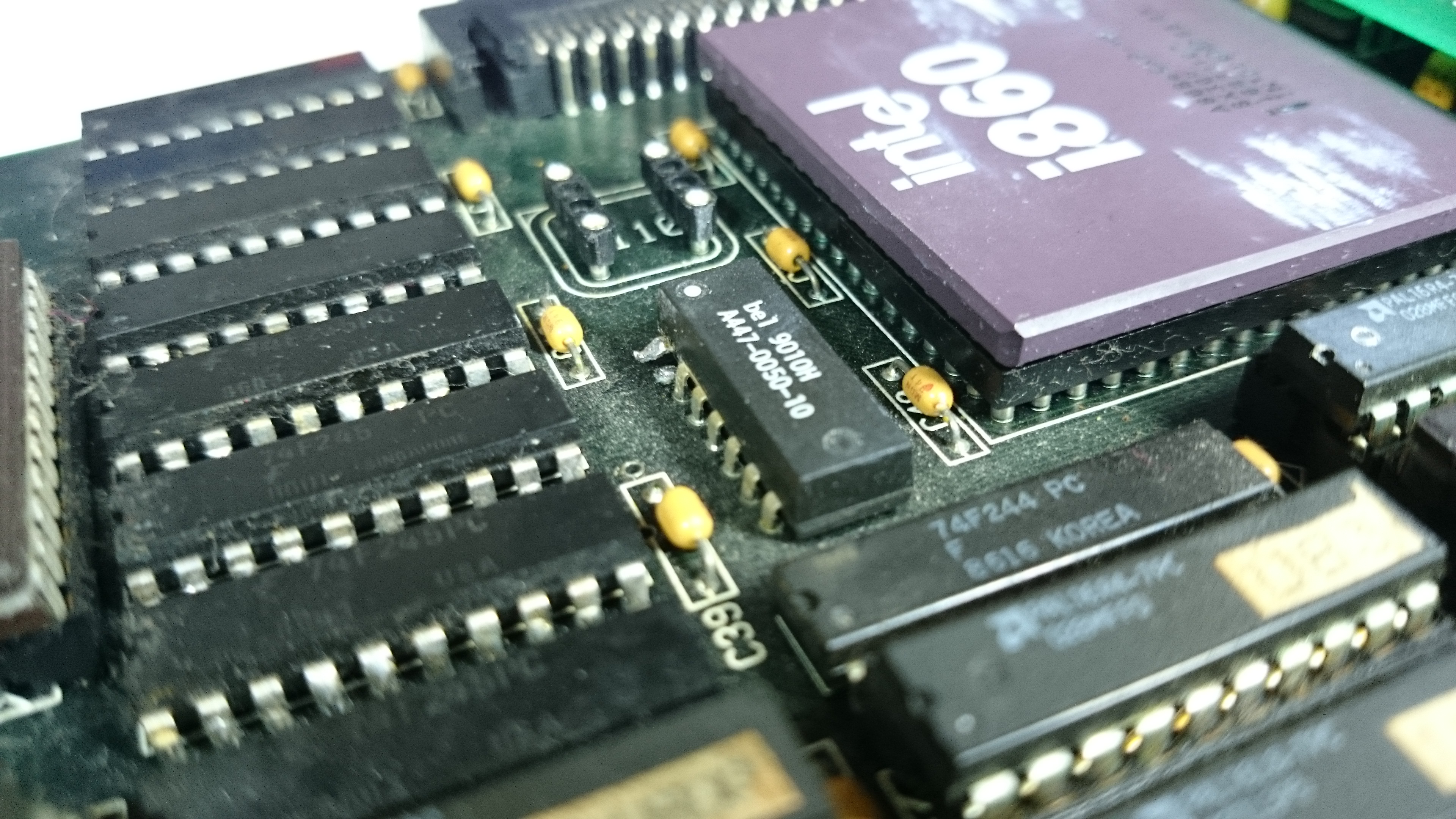
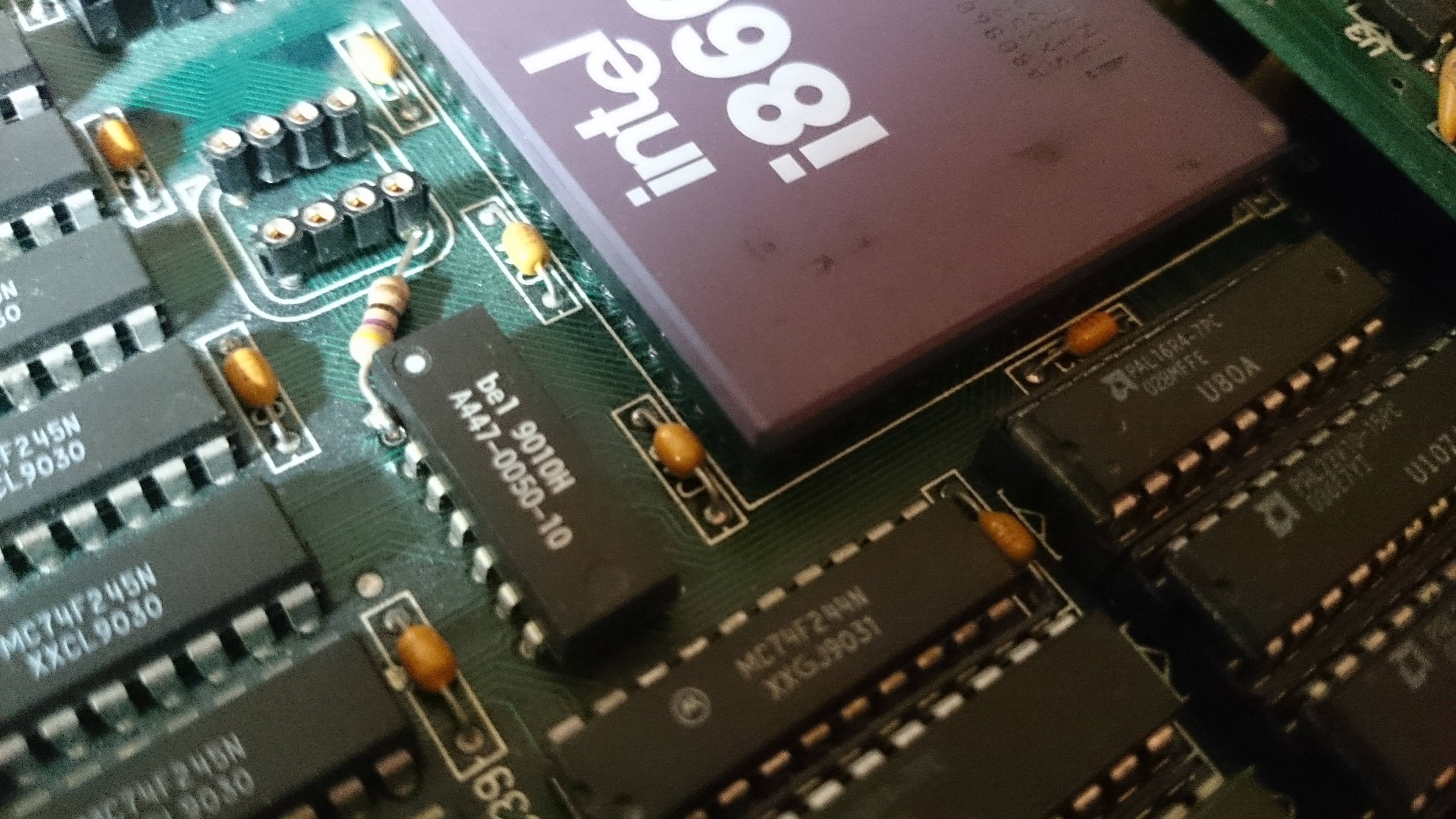
Here’s the left side in more detail:

DSM860-16_left

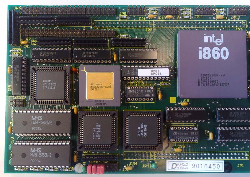
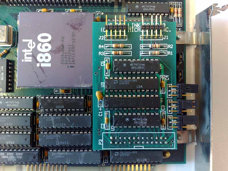
This end of the card is the “external comms” side. Beside the all-mighty i860 you can easily spot the golden Transputer being the communication controller.
To its left, there’s the first dual-ported RAM (1k x 8) connected to the socket for the external bus (Ring-A, located on the edge above). Below that are the two 16k SRAMs -marked MHS- for the Transputer. Then to the right are the two dual-ported RAMs (a 7C131 and a so-called slave 7C141) making the 16-bit connection to the i860’s bus. The rest of the parts are quartz oscillators (5MHz & 40MHz) and drivers/buffers for the buses. On the top edge next to the Ring-connectors you can spot the 4 Transputer links (JP9-12).

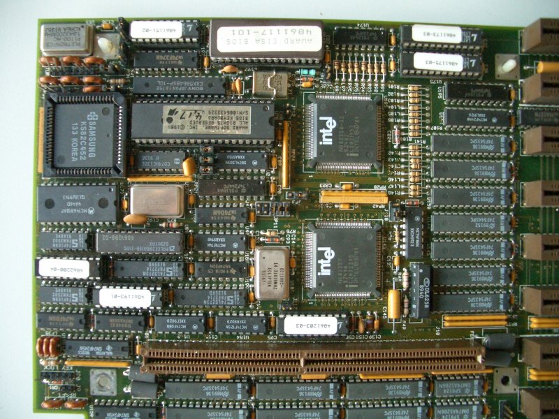
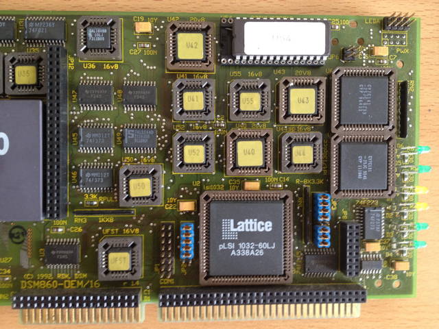
The right side is comparably boring:

DSM860-16_right

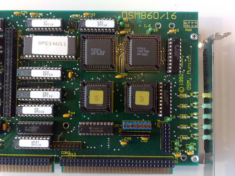
The boot EPROM, 6 GALs, again two dual-ported RAMs (this time for the ISA-bus connection) and some buffers… well, and 5 LEDs. LEDs are good. 😉
Also, you can see the pin-row connectors at the lower edge and on the left of the photo. That’s the expansion-bus. The lower connector is more or less 1:1 the ISA bus, the left one is a 16-bit bus to the i860. AFAIK, they never offered an expansion for sale.
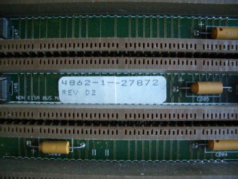
The last (but not least) interesting thing on this picture is the copyright. Yes, it’s a DSM860/16 from 1992, RDK made it (Rolf-Dieter Klein), DSM in Munich distributed it – but it’s obviously also a rev. 1.6, which means there could be others before or after that one. If you have more informations I would be happy to learn more.

DSM860-OEM/16

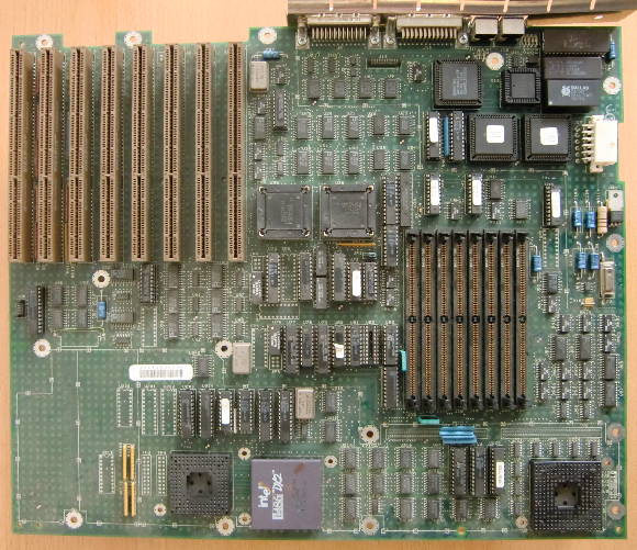
I’m pretty sure there was one more version after this rev.1.6, this b/w picture from a DSM press release about shipping the 250.000th slot-CPU card shows a very changed design. The silkscreen print says “DSM860-OEM/16”, so it’s obviously nothing for the normal market.
Mind the onboard-RAM, the missing comms-section and the high integration (SMD parts all-over) and even an early form of an FPGA from Lattice – my assumption is that this version could be the answer to the Kontron SBC860 showing nearly the same layout:

OEM_250ste
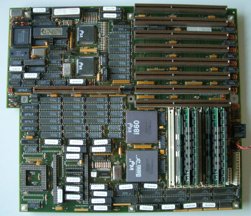
At least this ‘riddle’ is finally solved. I was able to buy an DSM860-OEM/16..Yay! As assumed, it is a modern (for 1990 standards) version of the DSM860-16 now consisting of just one board, so no more RAM card as described below- and without the Transputer and Ring-A/B stuff.

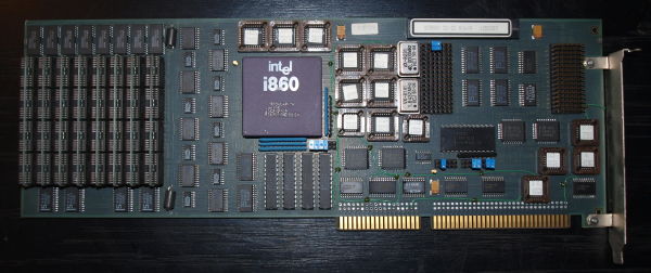
Here are my pictures of it. First of all, the card in full view:

OEM16_full

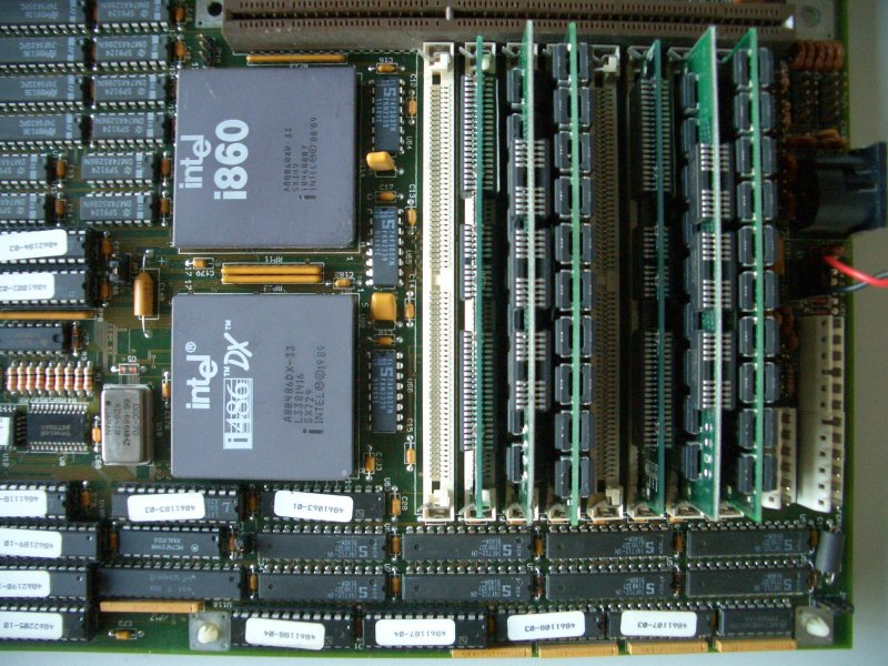
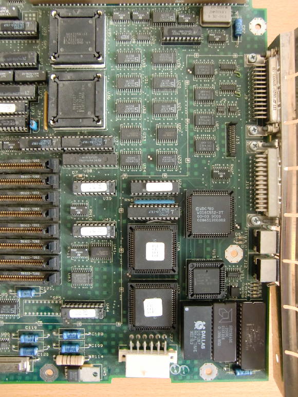
The right half shows a very high degree of integration compared to its predecessor. All DIL ICs were replaced by SMD parts and lot of logic went into PALs and even an FPGA (The contents of the EPROM is the same as with the other card, minus Transputer handling):

OEM16_right

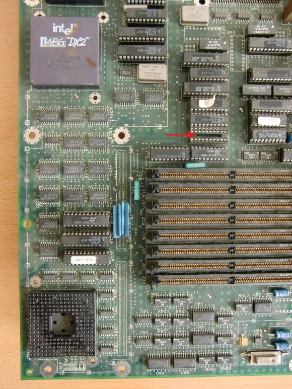
The left half contains the CPU and the RAM. This time only 8 SIMM slots:
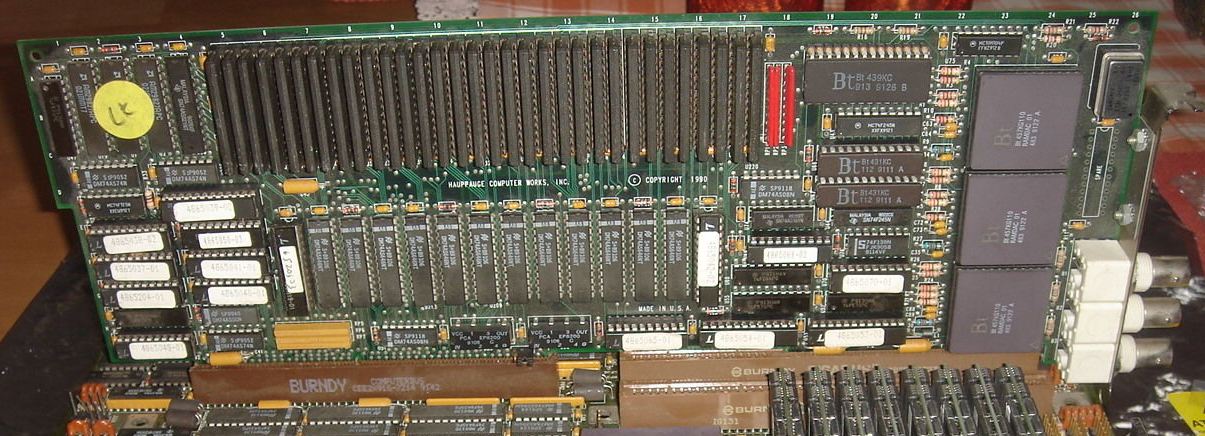
OEM16_left

The RAM card

DSM860-RAMcard

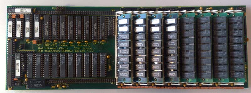
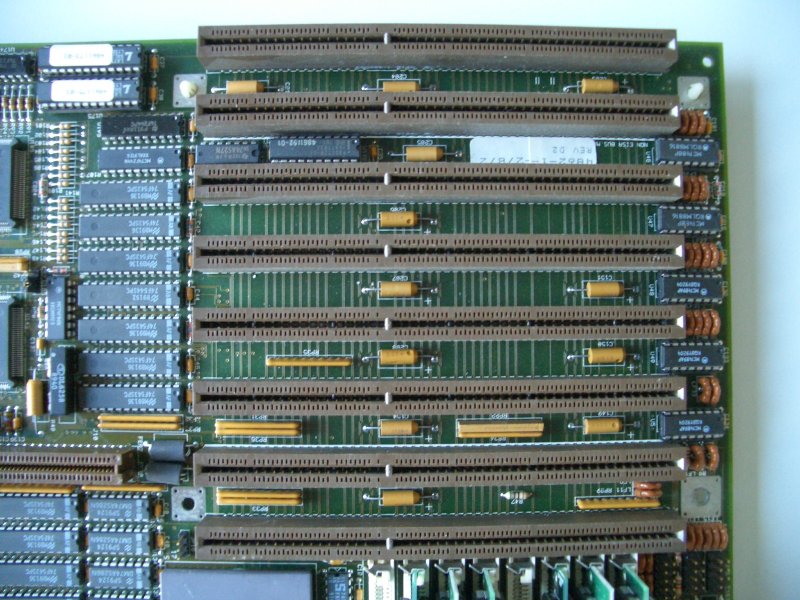
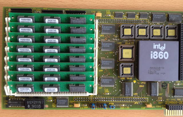
This is the 2nd part of every DSM-860 – the RAM card (except the OEM-16). Same dimensions as the SPC itself… i.e. full length. The biggest part of it is consumed by the 16 angled SIMM sockets, obviously interleaved, thus named altering slot-a & b. Only the 8 a-slots are populated on mine.
The rest of the board is used for lots of buffers and drivers, some GALs (doing the mem-mapping) and there’s quite a big copyright… again.

DSM860-RAMcard_C

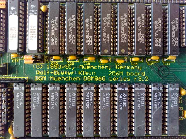
One typical detail of those days is the fact that manufacturers were not very keen on having users doing upgrades themselves. Even this RAM board has standard SIMM sockets and one could simply plug in more SIMMs to expand the RAM you had to change a GAL (the one in the lower left corner with a while label saying “UXM24Wxx” on it). Obviously these GALs are the only ones notdocumented. All I know is that there were 3 GALs available differing in the last two letters of the label:

  • 8B = only a-slots can be used by either 1M or 4M SIMMs giving 8 or 32MB total
  • 16 = both a- and b-slots used with 1M SIMMs = 16MB total
  • 64 = a- and b-slots filled with 1M and/or 4M SIMMs giving 16, 40 or 64MB total.

Because the card as well as the documentation says the maximum supported amount of RAM is 256MB there might be the chance of supporting 16MB SIMMs – I did not try this yet.

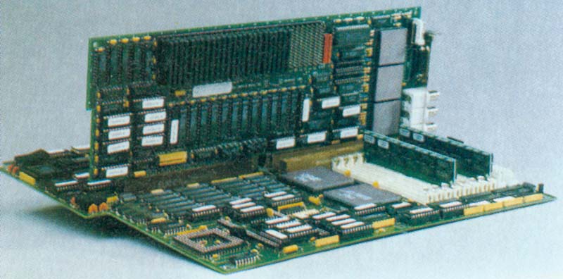
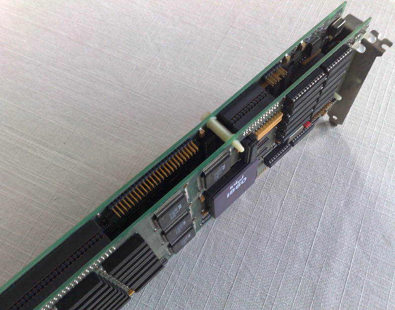
Both cards attached together give quite a big and heavy sandwich

DSM860-16_sandwich

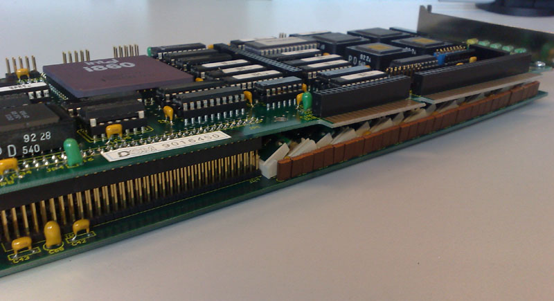
It’s obvious that you not only need 2 full-size slots but also guide-rails inside the case to hold the weight of this beast.

DSM-860/32

This seems to be the king of the SPC hill. Technically it’s pretty much the same as the DSM-860/16 but this time featuring a 32-bit system bus – namely EISA. The EISA bus was a dead-end like IBMs Microchannel but comparably easy to implement and free of license fees.

So the main difference to the DSM-860/16 is the 32-bit wide connection to the hosts bus, visible by the 4 dual-ported RAMs used for a 32-bit wide connection to the EISA slot.

Again, here’s a 1992 magazine ad showing a probably early version of the card as the marking says “DSMß860-32” (mind the beta) and the year “1991”:

print-DSM860-32

Compared to that, my version (1.2) does not look that much cluttered – also the Transputer comms part were moved to the left side of the i860 and two more LEDs were added:

DSM860-32

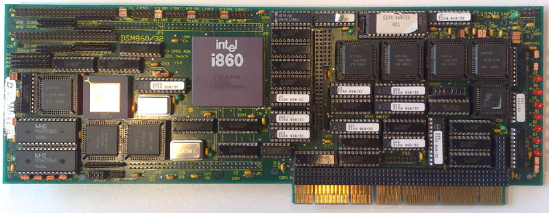
So the left side of the card looks pretty identical to the DSM860-16, while the right side has a bit more logic to satisfy the EISA standard, the already mentioned 2 more DP-RAMs, a bigger expansion-bus due to the EISA slot and most important: 2 more LEDs! Did I mention that LEDs are good? 😉

DSM860-32_C

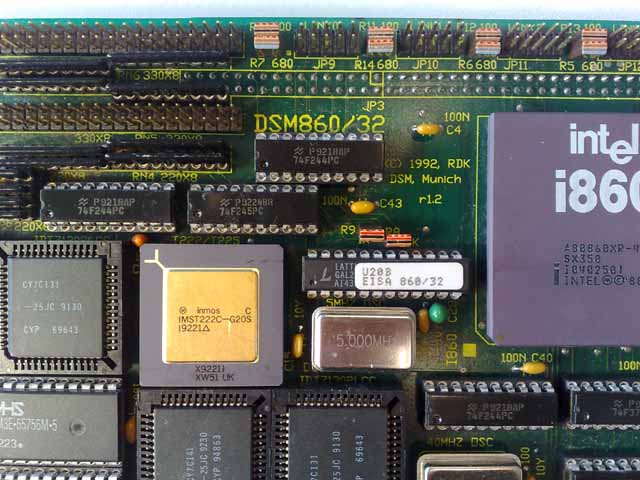
This more detailed picture shows that the DSM860/32 was released the same year as the ISA version. This card is a rev.1.2 – again, if you know more about revisions, I’d be happy to hear from you.
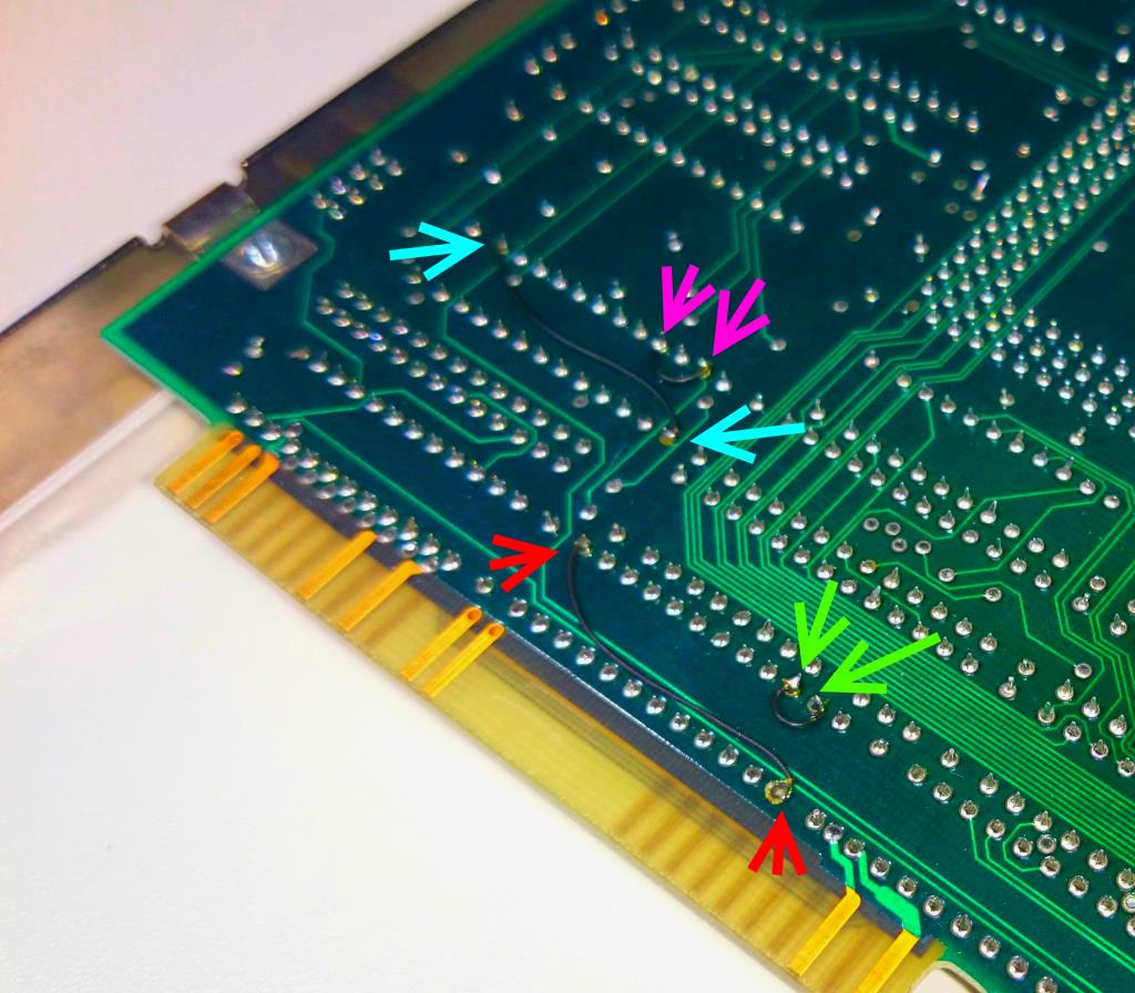
You might have spotted that this card looks a bit shabby. That’s because it was pulled from some universities dumpster. It was missing some components and had some “scars”. The good thing was that none of the GALs were missing and due to the fact that every piece is documented on the card it was easy to replace the missing parts.
On the above picture you can clearly see e.g. the 100nF capacitor C40 below the i860 or the 40MHz OSC. I wish everything would be that well documented.

The Infinity card

This is a rare and mysterious beast. The documentation only touches it very briefly. It’s definitely nothing been built for the average DSM860 user – if something like that existed. For sure it was extremely expensive… and it has LEDs 😀

DSM-EINF860M

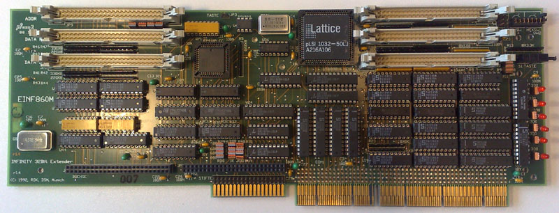
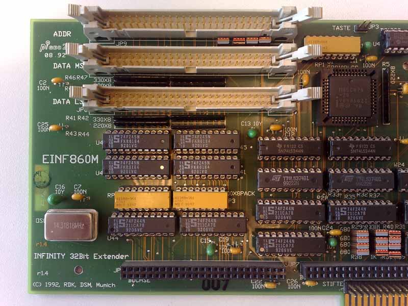
So at the first look you see 2×3 connectors for 40pin cables – the same used on the DSM860 cards (Ring-A and -B). Then there are a lot of drivers and buffers and a big Lattice pLSI 1032-50 which is a 6000 gates PLD (Programmable Logic Device). A closer look to the board gives more hints – thanks to the DSM (or RDK) habit to print as much info as possible onto the board:

DSM-EINF860M_C

Ok, first information we get is that this is a EINF860M or INFINITY 32Bit Extender. It’s like all other boards (c)1992 by DSM Munich and -as one would expect- designed by Rolf-Dieter Klein (RDK).
The three connectors are labeled ADDR(ess), DATA MSB (Most Significant Byte) and DATA LSB (Least Significant Byte).
The the right of the connectors is an Intel 85C098-20. I think that’s a One-Time-PLD, not 100% sure.

My educated guess is that this card is what the print on it says: A bus extender. Using the 16-Bit bus on the DSM860 cards one can build quite a big parallel computer. But the max. length of the flat-cable to connect each card with the next one is limited. So this card would be connected to other DSM860 cards in the same case (i.e. a 19″ case in a rack) and the extender would then “amplify” the bus-signals to be send over into the next rack full of DSM860 cards.
That said, my fear is, you’ll need two of those cards as the seperation of Adresses and Data (MSB and LSB) is nothing being used on the DSM860 cards. So my next guess is, that the INFINITY communicates over the EISA bus with the other cards and has its own external bus. Again – I’m happy if you contact me if you know more/better!
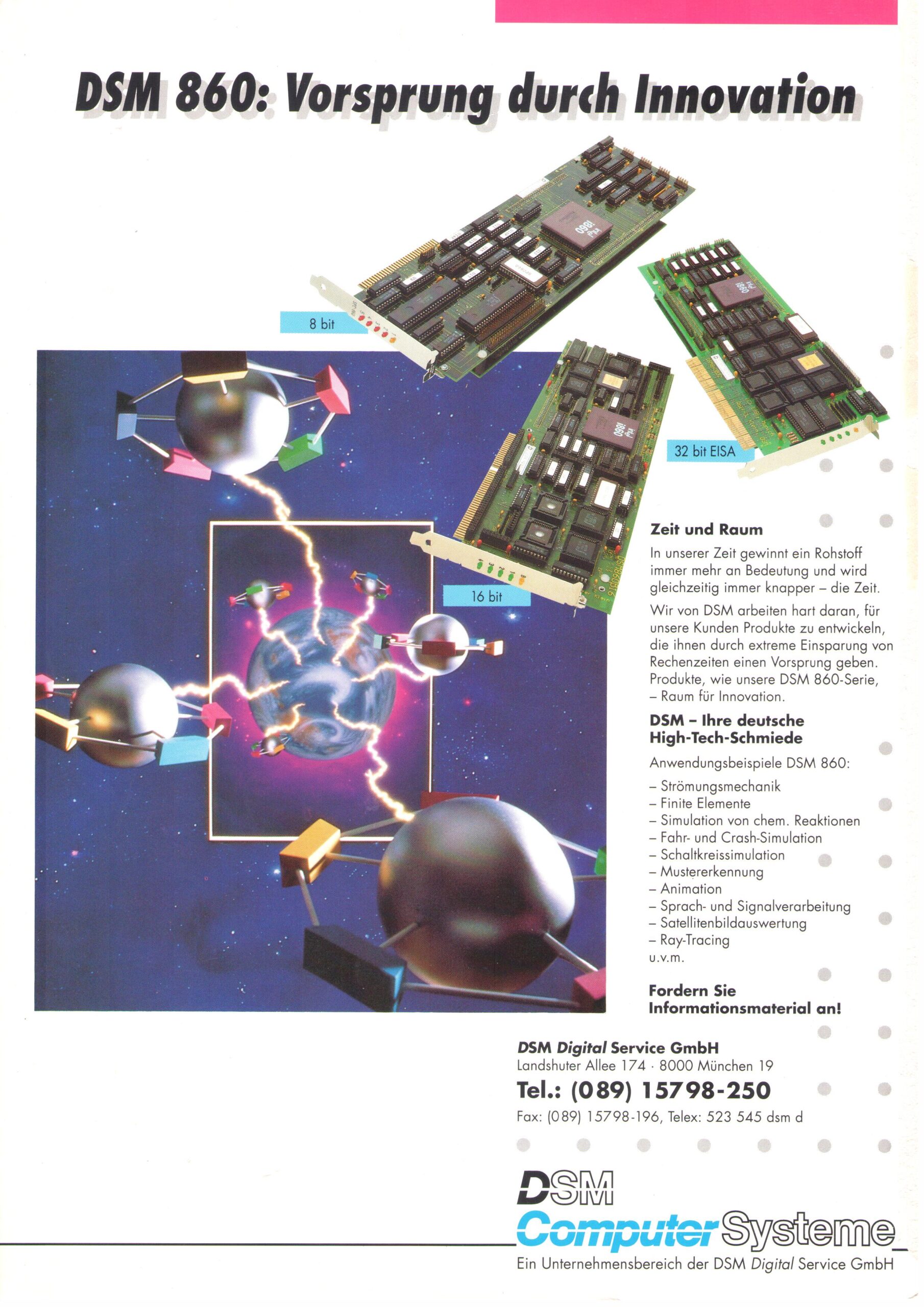
Nostalgia

And here’s a full page ad I found in my old (German) computer magazines – it shows all 3 versions:

Dissection time!

Ok, as I’m probably the last person on this planet fiddling around with the NumberSmasher i860, it was either “help yourself” or bust.

Given the fact that there’s an INMOS C012 on the card I tried my luck with the standard address of 0x150 and checked it with DOS’ crappy old ‘debug’. To my surprise I was able to talk to the C012, so it was very worth to investigate further.
So out went the good ol’ EPROM programmer and the EPROM of the card was dumped into a file.
I have 3 of those boards, two having a label on the EPROM saying “v1.1” and “BOOT_B2”. Both are identical… if you happen to own a NumberSmasher with a different label, get the dumpfile here for comparison.

That was easy, now the harder part: Disassembly. I had to revive my i860 machine language skills again, so it took me 2 days (on and off) to get a full understanding, what’s happening in there.
For those i860 assembly geeks among you, here‘s the fully commented code.

This “BIOS” is actually pretty simple. It’s just what I’d call a “PeekPokeStarter”. The main loop is waiting for a ‘command’ coming in by the way of the C012. This command can be either “0” or “1” as mentioned in the article on the previous page.

“0” means POKE (ie. write) and expects 4 bytes for the address and 4 bytes of data to be written (Both LSB first, Intel-style). So the full command reads: 0 00 00 00 20 78 56 34 12 or “write to address 0x20000000 the value 0x12345678”

So in consequence “1” means PEEK (ie. read) which just needs 4 bytes for the address to be read. The command would then be 1 00 00 00 20 or “read from 0x20000000”. The “BIOS” will then put 4 bytes to the C012 port at 0x150, which requires 4 reads from the PC side getting “78”, “56”, “34” and “12”.

Pretty simple, huh? But how can I start a program after it’s been painstakingly poked into the NumberSmashers RAM? Here’s the trick:

Poking to address 0x00000000 means start from the address given as data. E.g. “write to address 0x00000000 the value 0x20000000” is actually “start from 0x20000000”, or as command-chain: 0 00 00 00 00 00 00 00 20 – so beware of poking to 0!
Also, starting a program seems to disable the EPROM, so communication to the C012 is cut off if the running program isn’t handling this itself.

That’s about it. Nothing more in the “BIOS”… that’s why only 495 bytes(!) of the 8K EPROM are actually used. This simplicity leads to a very simple memory-map:

Base =  0xF8000000
C012-InData = [base] + 0x07
C012-OutData = [base] + 0x0F
C012-InStatus = [base] + 0x17
C012-OutStatus = [base] + 0x1F

Next task: Get a program running on the NumberSmasher.

[11/11/10] Great News…again! It was easier than expected… the first program running on the NumberSmasher-860! So read on in the next post…

Run Forest, run!

After having figured out the basics, it was time to prove the concept. First, I needed a (simple) program to run on the NumberSmasher. Here it is, reeeeally simple. It’s just an excerpt of the original 77 assembly lines. If you’re interested in the whole thing, it’s here.

The main-loop is just this. Read a byte from the C012 link, add 1 to it and write it back to the C012:

mov    iobase, %r4

loop:
  call    getlink        # (watch following delay slot!)
   shl    %r0, %r4, %r16    # mov r4, r16 - save base address

  addu    1, %r16, %r17    # add 1 and move into r17

  call    putlink        # (watch following delay slot!)
   shl    %r0, %r4, %r16    # mov r4, r16 - save base address

  br        loop
nop

What a task for a “Cray on a chip”! 😉 Ok, putting this into the assembler (currently gnu-as on Linux), linking and finally making it a pure binary with ‘objcopy -O binary hb_test.cof hb_test.bin‘ I got this binary.

How do I get it into the NumberSmasher? Again, that required a bit of coding… say Hi to nc_load.exe.
This little tool loads a pure i860-binary, pokes it into the NumberSmashers RAM and optionally starts it afterwards, ie. ‘nc_load hb_test.bin 20 start‘ loads my test program to address 0x14 and starts it from there.
[Having read the previous post, you should know that you could omit the ‘start’ parameter and just poke 20 to address 0 to start the code]

Test, test, one, two, three…

And now the exciting part: Does it work? The easiest way to test this is good ol’ debug again:

C:\> debug
-o 151 41
-i 150
42

Yay! If this isn’t proving the sense of life, what else!?!? 😉 Ok, what happened here is simple. I wrote 41 to port 151 on which the C012 is listening for input, then I read from port 150 which is the result of adding 1 to the input. Quod erat demonstandum. Program is running successfully!

Be aware that after starting a programm, the NumberSmasher is continously running that code, i.e. peek & poke do not work anymore because the Boot-ROM is out of the game.
You have to reset the NC which is done in classic INMOS-style, i.e. sending a zero to port 0x160. Thats ‘-o 160 0’ in debug. NB: Resetting the NC does not clear its RAM. The previously uploaded program is still available and can be re-started by pokeing the start-address to 0.

Olivetti CP486

The Olivetti CP486 was “the other” machine on the market which provided an 80486 and an 80860 on the same mainboard. The same board was used in Olivetti machines called LSX-5010 (25MHz) or LSX-5020(33MHz).
Like the Hauppauge 4860, it was an EISA bus system too, had no 2nd level cache but an extra socket for a Weitek 4167 FPU. Again very similar is the use of an huge array of PALs and GALs… and huge is the keyword for its size:  40,5 cm x 34 cm (16″ x 13.4″)!

CP486_total

My CP486 which I’m showing here seemed to have been through very though conditions. It was quite dirty and is of course not working :-/ Mainly due to a missing PAL, I guess (shown in the following picture).
So here’s the lower part of the board (90° tilted for better reading):

CP486_left

At the top the i486, in this case an DX2/50 I had lying around – nicely fitting the 25MHz oscillator to the right of it. At the edge of the photo you can see a bit of another socket. That’s where the optional Weitek FPU would have go (See the picture of the total view).
Next you’ll spot the many PALs around it. And a wild mixture it is! All PALs/GALs on the board are from different manufacturers, years and kinds. Some still featuring labels, most of them peeling off. According to the only documentation I was able to find, “in field” upgrades seemed to happen quite often. The little red arrow indicates the missing PAL at “U82” I talked about before. It should be a 16R4 containing the snoop-control, a vital part of the memory management. Without it, the board is pretty much brain-dead 🙁
Next are 8 slots for PS/2 SIMMs… depending on the BIOS version up to 64MB RAM were usable.

In the low left corner is what made this board special: The i860 socket. The 3 PALs above it are his address decoders… nothing is known about how the two processors shared the RAM.

Which leads us to the other half of the board:

CP486_right

This part is mainly chip-set stuff. At the top left there are the Intel 82358 EBC and 82537 ISP (See my Knowledge-Base article for more info) ICs.
The rest of the action is squeezing into the lower right corner: On top the WD16C552 Serial and Parallel Port Controller. The other two bigger PLCC ICs are EP1800 CPLDs supposedly working as I/O controllers. To their right is a 8742AH handling the PS/2 keyboard and mouse.
Below that there’s the inevitable DALLAS clockchip, a 64kbit EEPROM (probably EISA config) and a 1Mbit 28F010 Flash EPROM for the BIOS. Pretty modern stuff actually.
Naturally I read out the BIOS… it’s completely Olivetti propriety as they always did back in those days (Download available at the end of this page).
Last but not least, the power connector. Again, propriety but I do have the original power supply. Nice big paper weight.

The EVC-1

Like the Hauppauge 4860 (again), the CP486 also offered a special Graphics Card which enabled the i860 to directly write into its video memory, so it could be used as an accelerator.
While Hauppauge went the way of offering a special dedicated slot, Olivetti designed a special EISA Video Card… well, the EVC-1.

CP486_EVC

While it features a standard EISA slot connector, it does not work in other EISA systems (You get the BIOS boot messages but it then hangs with wire-do chars displayed).

It’s core is a Chips & Technologies 82C452, a mediocre VGA chip.  Olivetti attached this DRAM VGA controller to 1MB dual-ported DRAM… This totally makes sense because the 82C452 can act as a simple VGA controller while the i860 will als be able to write to the screen (via EISA DMA) for example doing the heavy lifting graphics stuff. The idea is the same as Hauppauges Framebuffer but enhanced with a VGA controller.
That said, IMHO 1MB video memory is a bit less for such a professional approach.

Conclusion

So, here‘s the CP486 PDF-document I was able to find in the WWW including my BIOS dump.
If you happen to own a CP486/LSX50x0 I would be happy to hear from you!

Final anecdote: I’m not sure this guy (German forum, Google-Translate will most likely help) knew what he was doing when scavenging a complete, fine running LSX-5020 for a boring case-modding stunt. In a few years he will kick his ass for killing a one-of-a-kind machine for a boring mass-market PC.
That’s the same sin many Americans did to their vintage Ferraris when they replaced the somewhat complicated original engine with an off the shelf Ford V8 to make it reliable… and reduced its value to 10%. Sin! Sin I said!

Putting the DSM to use

So after the lengthy description of the DSM cards – how can we make use of them? As said in the previous chapter, they were shipped with an assembler and even an early version of GCC (1.3) so development is pretty straightforward.

Activation

First, you have to understand how the cards integrate themselves into an ISA/EISA system. While the three versions (8, 16, 32bit) differ in some areas, the integration is more or less similar:

Each version offers a latch for controlling the card. This means to activate the card by writing bits to that latch to define a memory-window inside the hosts RAM to blend-in the cards dual-ported RAM  and/or resetting it etc.. The latch is accessible through an IO-port set by jumpers on the card (default 0x300).

So for the ISA cards you have to for example write a 0xC2 at that port-adress to reset & activate the card and use the mem-window of 0xDC000-DC7FF. In Turbo-Pascal this would be something like:

port[$300] := $c2;

This gives you a 2K mem-window to exchange data between the DSM and the host (just 1K for the DSM860-8).

The EISA cards obviously use other ports depending on the slot-number, so this would be an example to do the same for am DSM860-32, this time in Turbo-C:

outportb(slot_no * 0x1000 + 0x800, 0xc2); // For slot #2 this would be 0x2800

This would also open a mem-window at 0xDC000, this time up to 0xDCFFF, i.e. 4K long.

Memory

As mentioned above, the Host and the DSM-card are communicating through a memory-window of diffenrent sizes, depending on the DSM used. Due to their nature, the memory is looking different though. That said, at least they’re both litte-endian, so no byte-swapping needed.

The 80×86 side

For the hosting PC, memory looks pretty straightforward. 1KB-4KB of RAM somewhere in ‘lower-RAM’, that’s it.
While we don’t use it, it’s worth mentioning that there’s a 2nd memory window called “Common“. This is fixed at a specific address and is shared between all possible cards plugged into one host. I guess you already got it: This enables easy multi-processor communication… and gives a lot of possibilities for f**k-ups.

The i860 side

The memory-mapping on the i860-side is the same for the 16 and 32bit cards, the dual-ported RAM is located at 0xd0040000 (0xC0000000 for the DSM-8).
In any case the i860 memory is linear, 64bit wide and always on a 64-bit boundary. This means you have to read the DP-RAM area differently depending on which card you run your code. Here’s an example of how the DP-RAM looks like on the Host- and i860 side:

Host DP-RAM in DOS ‘debug’
-d dc00:0000
DC00:0000 11 22 33 44 55 66 77 88 ...

which would look like this on the i860 side:

DSM/8
C0000000 - 11 xx xx xx xx xx xx xx 22 xx xx xx xx xx xx xx
C0000010 - 33 xx xx xx xx xx xx xx 44 xx xx xx xx xx xx xx
C0000020 - 55 xx xx xx xx xx xx xx 66 xx xx xx xx xx xx xx
C0000030 - 77 xx xx xx xx xx xx xx 88 xx xx xx xx xx xx xx

DSM/16
D0040000 - 11 22 xx xx xx xx xx xx 33 44 xx xx xx xx xx xx
D0040010 - 55 66 xx xx xx xx xx xx 77 88 xx xx xx xx xx xx

DSM/32
D0040000 - 11 22 33 44 xx xx xx xx 55 66 77 88 xx xx xx xx

So reading and writing from/to the DP-RAM involves some thinking to be done by the programmer. Here are two code-snippets showing the difference between reading the DP-RAM on a DSM860-8 and an DSM860-16. First the ‘8 bit version’:

mov 4*8,r4
readloop:
ld.b 0(r15),r14  // Load BYTE from DP-RAM
st.b r14,0(r29)  // store it destination
addu 8,r15,r15   // add 8 to read-mem-pointer
addu 1,r29,r29   // add 1 to desitination-mem-pointer
addu -1,r4,r4    // loop-counter
xor r0,r4,r0     // Test Zero
bnc readloop

And the same for the DSM860-16:

mov 2*8,r4
readloop:
ld.s 0(r15),r14  // Load SHORT (2 Bytes) from DP-RAM
st.s r14,0(r29)  // store it destination
addu 8,r15,r15   // add 8 to read-mem-pointer
addu 2,r29,r29   // add 2(!) to desitination-mem-pointer  (short <> byte)
addu -1,r4,r4    // loop-counter
xor r0,r4,r0     // Test Zero
bnc readloop

Because of reading SHORTs (ld.s) the DSM860-16 version has to loop just 16 times while the 8-bit version has to do that 32 times.
Same applies to writing. You will find an example in the Mandelbrot program (Commented source file).

[This is work-in-progress and will expanded over time]

Action!

So here we go, finally some program running showing all the power behind the i860. I took the Mandelbrot example from R.D.Klein and modified it a bit, well quite a bit as it was written for the DSM860-8 and provided CGA output (yuck!).

Like most “external accelerator” programs, there’s one part running on the accelerator (the i860 in this case) and one part running on the host doing useful things with the provided data. In this case we have an i860 assembler code doing the number-crunching on the Mandelbrot algorithm using the i860’s ability of ‘dual instruction-mode‘ and some code done in Trubo-Pascal handling the display and zooming.
The latter was extended to use SVGA (640x480x256) output and providing an interrupt driven timer. [sourcecode package cleanup is still work in progress]

Here are the two running full steam ahead:

Some things worth to mention:

  • The host being used here is a P1 133MHz, a bit unfair comparing that to a 40MHz i860 – OTOH they seem quite comparable when it comes down to Mandelbrot crunching speed.
  • To calculate the Mandelbrot the same speed as it took the Pentium (~15s) I needed five T800-20 according to my benchmarks.
  • To even achieve the 8.2s of the i860 I had to run 9(!) T800-20 in parallel.
  • A i486DX/33 took 66 sec to do the same (8.25 times slower!), while it still took 34s for a i486DX2/66!

So while all that moaning about the bad ‘programmability’ and slow context-changes of the i860 are completely correct, in certain tasks that CPU was indeed a real screamer!

Upgrading the NumberSmasher

After a long time, I had a look at my 3 NumberSmashers again. Looking closer, I spotted a difference.
One had a silkscreen print saying “V1.2” while the others were “V1.1”. So why not upgrading the NumberSmasher yourself?!

Step 1

The most obvious fix the V1.2 had was a 47ohm resistor fitted between one pin of the 40MHz oscillator and pin-1 of an IC called “A447-0050-10 “. That’s a “10 tap leading edge delay module” made by Bel Fuse Inc.. Pin 1 takes the input signal and each other pin  adds a delay of 5ns.
So I assume this fix was meant to reduce noise on the delay chip input to make its output cleaner.

Anyhoo, here’s the quick and easy howto. The below picture shows the section of a NumberCruncher V1.1. near the almighty i860. Next to it is the (now empty) socket for the 40MHz oscillator. Next to that you see the 10-pin delay chip which pin-1 already had been cut and slightly bent upwards.
We need a bit of pin-1s leg so when cutting it, be sure to cut it as close to the board as possible!

NS_premod.jpeg

Now for the next step. Get a 47ohm resistor and shorten its wires to bridge the space between the bent leg of the delay chip and the output pin of the oscillator (see below picture).

NS_860_postmod.jpeg

To make things perfectly clean, remove the pin remains by flipping the NS860 over and pull the remains with your solder iron and tweezers.

Step 2

I thought this would be a simple fix, too. There are some retrofitted jumper-wires on the back of the NumberSmasher near the ISA connectors.

NS860_patchwiresI’ve color adjusted the photo to make the wires more visible. Colored arrows show start and end of each wire

But taking a look at the chips those jumper-wires are connected, it showed that the two PAL22V10  of the V1.1 board were replaced by two PALCE610H – which is a completely different beast, same number of pins, everything else varies:

max in max out macrocells Specials
PAL22V10 22 20 10
PALCE610H 20 16 16  D, T, J-K or S-R Flip_Flops, counters and large state machines possible

Additionally here’s a side-by-side of the pinouts. This immediately explains the two long jump-wires from pin-1 to pin-13 (red & blue arrows) which connect the two clock inputs.

20v10_610h

Here’s the PALCE610 in place:

PALCE610It’s the one at the bottom in the middle (named U93) and one hidden beneath the link-interface board (U-88).

My assumption is, that the PALCE610 has a completely different programming and the jump-wires just support the changes made, i.e routing the outputs of pin3 to input pin2 (green) respectively pin4 to pin 2 (pink) .

Next up: I will get out my Über-Programmer and try reading it – but I have low hopes, as MicroWay normally set the protection fuse on all the GALs/PALs they used.

Update

Wow, that was unexpected. Both PALCE610 hadn’t had the protection fuse set – at least on my retro-fitted V1.1 board. So lo-and-behold, here are the JEDEC files for you to program your own PALCEs!  And because I couldn’t resist, I’ve disassembled the JEDs and added the PALASM code in the archive, too 😀

That said… it’s completely unclear what had been changed from V1.1 to V1.2 (well, U93 being close to the ISA connector gives a hint) and under which circumstances an upgrade is necessary at all.
But if you own a 1.1 and it behaves strange, you should give it a try.

Nostalgia

After the NumberSmasher, MicroWay presented the “QuadPuter”, an EISA-Bus based quad-i860 monster… which had a short lifespan and was, well, expensive as expected. 31000 German Marks was exactly what you would have payed for an Volkswagen Golf mkII GTI 16V back then… one of the hottest hot-hatches you could get.

I found this snippet in one of my (German) computer magazines (“MC”, 1993) – they mention the OS860 (for DOS) as well as the MAX860 multiuser-OS for UNIX, OS/2 and DOS: