All posts by Axel

http://www.geekdot.com/about-me/

RS422 Differential Adapter

This is a Q’n’D but handy design which I was planning for a long time, but you know how things go… A differential adapter is a simple device which translates a single signal/data line in one positive and one negative line, i.e. one is carrying the inverted signal of the other. This is also known as RS422… But why do we need such thing?

Well, differential signals are/were quite common in the world of Transputing to deliver OS-link signals over longer distances (<10m/30ft) or noisy environments and good examples are systems from Parsytec, the AVM-T1, ISA interfaces like the HEMA TA2 or even some custom measure/data-logging solutions.

So to connect to such systems using a non-RS422 (i.e TTL) interface card, e.g. the INMOS B004/008 or the Gerlach-Card you’ll need such an differential adapter.

Technical data

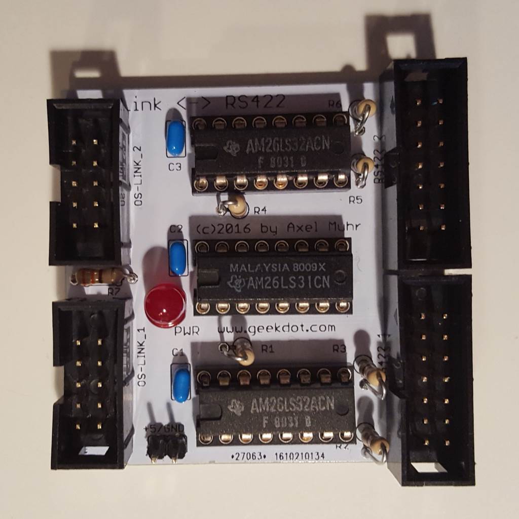
A very simple design on a 5x5cm PCB. All done in trough-hole technology (THT) to keep this a simple DIY project.
It all based around two AM26LS32 receivers and one AM26LS31 transceiver, some resistors and an unavoidable LED  😉

Usage is very simple, too. Just connect the TTL signals to the standard 2×5 shrouded PCB header connector and RS422 signals are provided on the 2×7 header connector on the opposite side of the PCB.
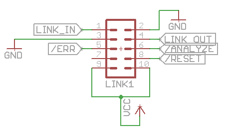
The TTL connector is the same as the one used on the Gerlach card or my T2A2 Apple II interface:

As you can see, pins 9 & 10 can provide 5V to the PCB so that no external power-supply is needed.
If you connect a system not able to provide power to the differential adapter there’s also a 2pin connector provided on the PCB itself.

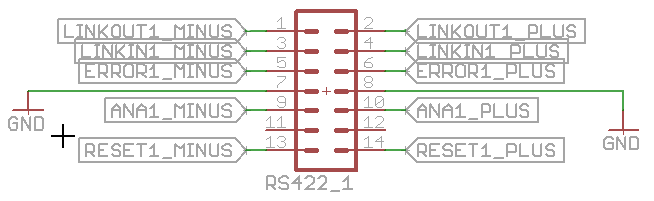
The RS422-side of the adapter has this pin-layout:

Nice-to-know: You could also use this adapter to simply invert signals. For example if you need a positive ERR signal instead of the not’ed, you simply take the positive pin (i.e. even pin-number 6 in this case) of the 2×7 connector (ignoring the negative).
Mind there’s no power supply pin on that side and pins 11/12 are not connected.

T2A2 for everyone

While the guys over at OpenApple were speculating in their latest podcast what a Transputer actually is… well, there are about a 100 links and ways on this page to find out – but hey… just click here – and of course that box saying search would do great wonders, too.

But seriously, my bad: I should have mentioned that this page your looking at is really just one post of many… so make sure you start at a Chapter (Menu. At the Top. ↑…yes up there) and read them in the order you’d read a book 😉

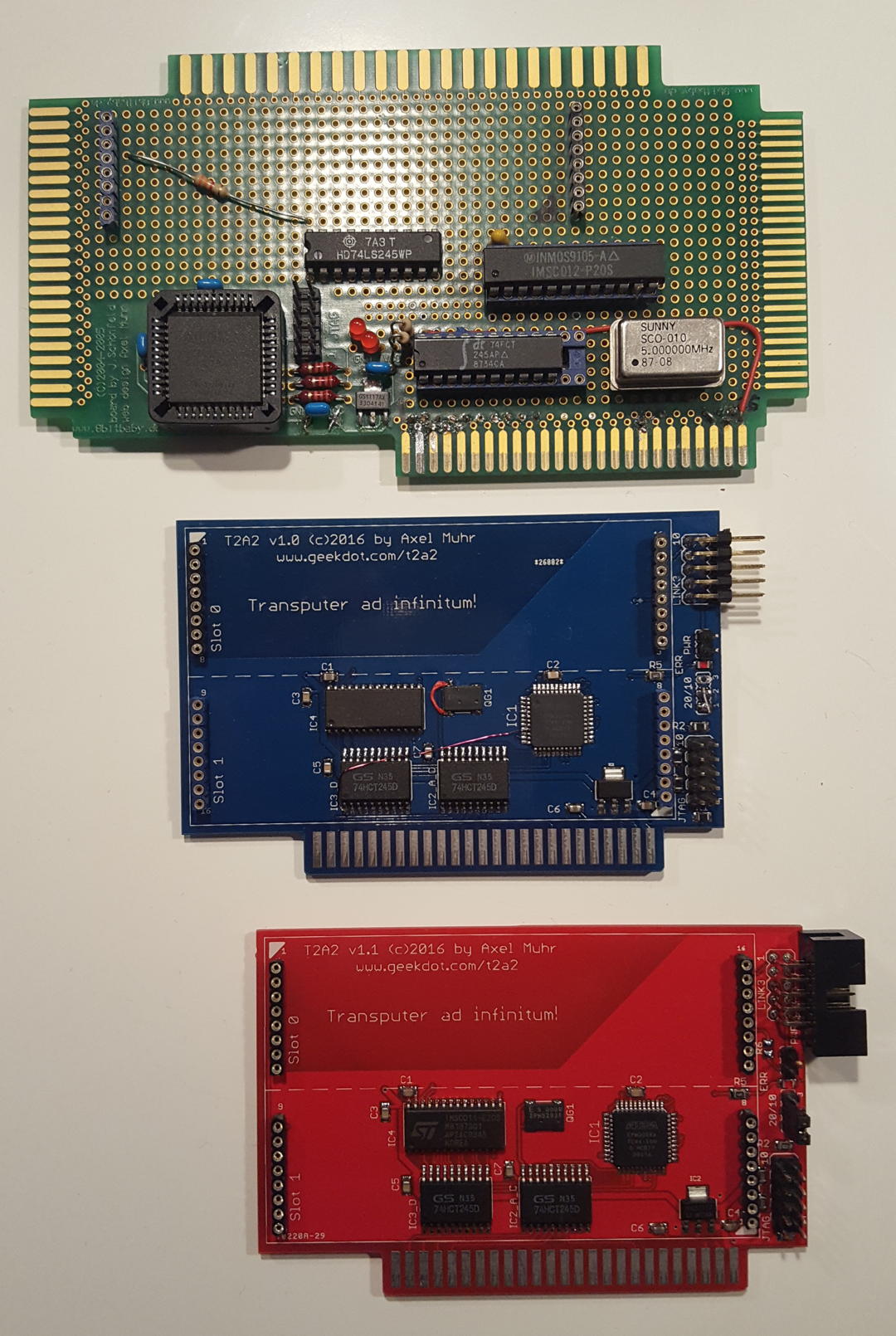
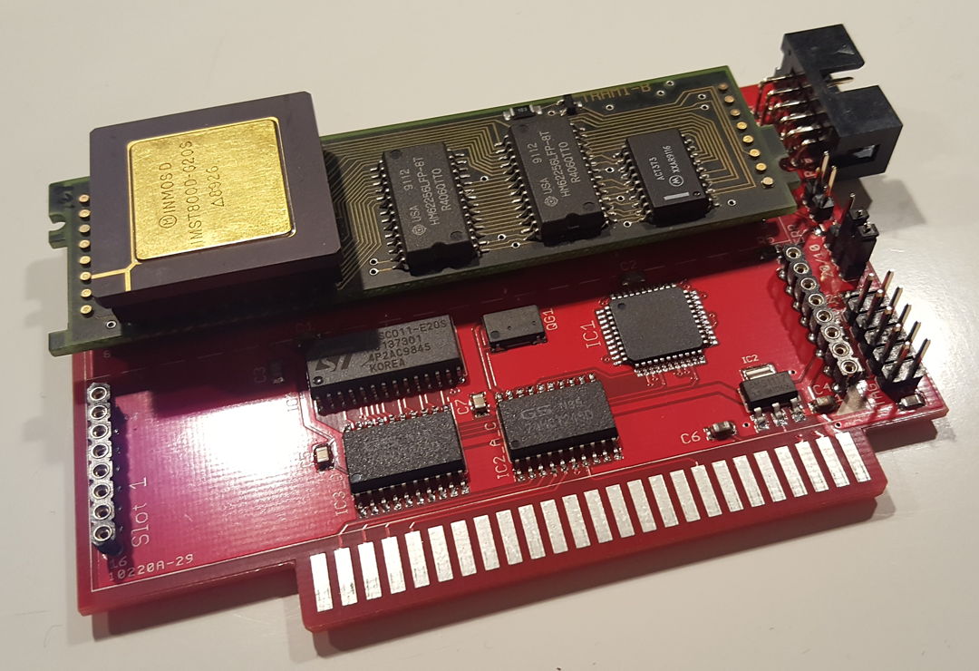
After quite some years (and a handful Apple II users requests) I felt the urge to finally put the T2A2 prototype (read that post to get a more general understanding) into a real expansion card… and here it is: Say “Hello!” to the T2A2 version 1.1!

It came a long way…

t2a2_evolution

…in more detail:

t2a2_front

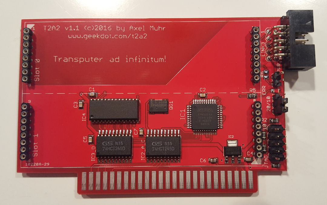
As you can see, the final T2A2 is much smaller than the prototype (which used an 8bit Baby one-for-all PCB) and offers many additional features

  • 2 size-1 TRAM slots (or one size-2) – double the processing power!
  • Low-power, low-profile parts used where possible (3.3V CPLD, HCT logic)
  • External Transputer-link available as edge connector – extend your network to “near infinitum
  • Jumpers for LinkSpeed and optional power to the Transputer-link connector
  • Fully buffered to be a good Apple II bus citizen
  • Works in any slot set to “your card”

Beyond this, everything said about the prototype is still true.

Most important:

a) It’s not tested in the ][ or ][+. I simply don’t own one of those.
Update: One owner reported it’s perfectly working in his IIe!
b) The T2A2 won’t instantly speed up any of your Apple II[e/gs] applications.

It’s more like a co-processor attached to it. And even then, you’ll need something really calculation-intensive to justify the time you’ll loose due to communication between the Apple and the Transputer. A single square-root for example wouldn’t make much sense – but having a complex algorithm (like the Mandelbrot fractal in my demo)  does absolutely make sense, as you just pass the parameters to the Transputer and let him do the sweating.

But on the other hand, FPU cards like the Innovative Systems FPE (using an M68881) or my even faster clone “NumberCruncher Reloaded” did just send instruction by instruction. So I somehow fancy the idea writing a SANE driver for GS/OS to integrate the T2A2 more transparently.

Want your own T2A2?

So now you’re keen to get one yourself? Please check this list first:

  • Do you have a TRAM already? (*)
  • You are aware that there’s no real software (yet) besides my little Mandelbrot demo?
  • You are keen to program something yourself – or are fine to wait until somebody else did?

While the Apple II side of coding is pretty easy, you have to get a grip about the Transputer development, too. That includes a DOS/Windows (<=XP) setup and some knowledge of C and/or OCCAM. I’ve created a little Transputer “SDK”, namely a VirtualBox image running DOS.

Plenty of Dev-Docs are available here.  
I suggest using the INMOS cross-compilers for C or OCCAM. An alternative C compiler came from LSC, which might suit you more if you don’t like the INMOS stuff.

Ok, so you’re still with me… so I have the first batch of 20 T2A2 PCBs ready which I will populate on-demand, and for 40€ (plus shipping) one of them can be yours.
(*) I might be able to offer you a TRAM, too. The price depends on available model, RAM size and CPU used.

⇒ drop me a mail tonobody likes SPAM
(Sorry, you have to type that into your mail-client – nobody likes SPAM, so do I)

Also check the T2A2 forum for current availability, shipping procedure and built status.

Some more technical details

Here’s a T2A2 with a size-1 TRAM installed in Slot-0:

t2a2_with_tram

The T2A2’s CPLD programming can be updated any time through a JTAG port (the lower 2×5 pin-row at the edge).
The jumper above it can be used to set the linkspeed for the TRAMs (10 or 20mbps). If you look very close, there’s a tiny LED next to that jumper. It’s the error LED controlled by the CPLD.
The next single jumper enables the VCC pins on the external Link connector, meant for (small!) external extensions. This connector is the same used on the Gerlach card and is very convenient because of its ubiquitous standard 2×5 shrouded pcb header connector. Here’s the pinout:

As said, the V1.1 T2A2 offers two size-1 TRAM slots. Before plugging in 40MIPS of raw processing power consider the amount of juice being pulled there. Depending on the amount of RAM and load a single TRAM can use up to 800mA of power!  😯
Given the max. of 4A on a standard IIgs power-supply, two TRAMs could bring your souped-up GS into trouble… it’s better to use the external connector with just one smaller TRAM or even simply bridge the Link0In/Out pins with Link3In/Out so that the T2A2 works as a TRAM-less adapter.
That said, there are size-2 TRAMs in existence which will snugly fit  and won’t hurt that much.

My new MacBook Pro from… Redmond!

F*ck me! I would never-neverever thought that this might happen… but last week was the time I switched to the dark side  😯

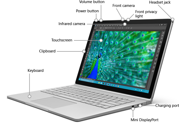
Say hello to my new “MacBook Pro”:

Whaaaat? Yeah, I know… but wait a sec before you pull your light-saber.

My Macs are both officially obsolete since macOS Sierra was released. A mighty 2008 Mac Pro as well as my 2010 MacBook Pro. Boy, believe me – did I anxiously wait for the presentation of the new MacBook Pro! That was in 2015… and ’16.. and then the big moment came. And went. I was, mhh, not impressed.
Many Mac users of the “first hour” complained about, well, everything. I have to say, I am a Macintosh user since 1984 – I moaned about the loading times of System 6 on a 128k Mac, I jubilated about the 1MB and SCSI in the “Plus”,  drooled over the IIfx, even admired  the doomed AV’s, ran A/UX, owned the first PowerMac etc.etc.etc… but this time, they just lost me.   😕

Missing ports aside (and I really need USB-A) the main reason for loosing me was the price they slapped onto the 15″ Pro… 2699€ – holy bat-wallet! That’s nearly $2900US$… $400 more than in the US. I was speechless. Angry. Flabbergasted.

So, after squinting into the Surface Book corner for some months already, I gave it a closer look (I quit using Windoze seriously when VIsta popped up) and had to admit that it helped Microsoft having been pushed into 2nd row. They at least got some things right and there’s always a VM with Linux at hand.
So I did it. Found an i5/8GB/256GB for a whopping 1000€ less and must admit: I like it a lot up to now. A speedy, stylish, well designed laptop, a big tablet and it natively runs all the FPGA IDEs, my logic analyser tool from china and Cygwin gives me an instant bash and GNU.

Never thought it would happen…. let’s see how it works out in the long run.

P.S: Apple Mail, I do miss you, though.

Did you drop your Macbook Pro dream, too? Think different? Post a comment!

T2shield – Arduino to Transputers

[The T2shield is currently a work-in-progress project – the first alpha hardware is operating but lots of coding lies ahead!!]

The idea for the T2shield was born when I thought about getting recent peripherals like SD-cards, Ethernet, displays etc. into a Transputer network.
Sure, there are the old, original TRAMs like the STM228 SCSI controller, the B431 Ethernet TRAM or quite some choice of graphics controllers. But they’re all rare like chicken teeth these days which means unaffordable when they rarely pop up on ePay.
Rebuilding them is also a no-no given the obsolete parts they’ve used… and to be honest: A noisy, vintage SCSI-1 drive isn’t what I thought of.
So after some time I came to the conclusion it will be the easiest and cheapest way to re-use what you can buy for a few bucks from China these days: Arduino shields.
As a lucky incident such a shield perfectly fits onto a size-2 TRAM – Yay!

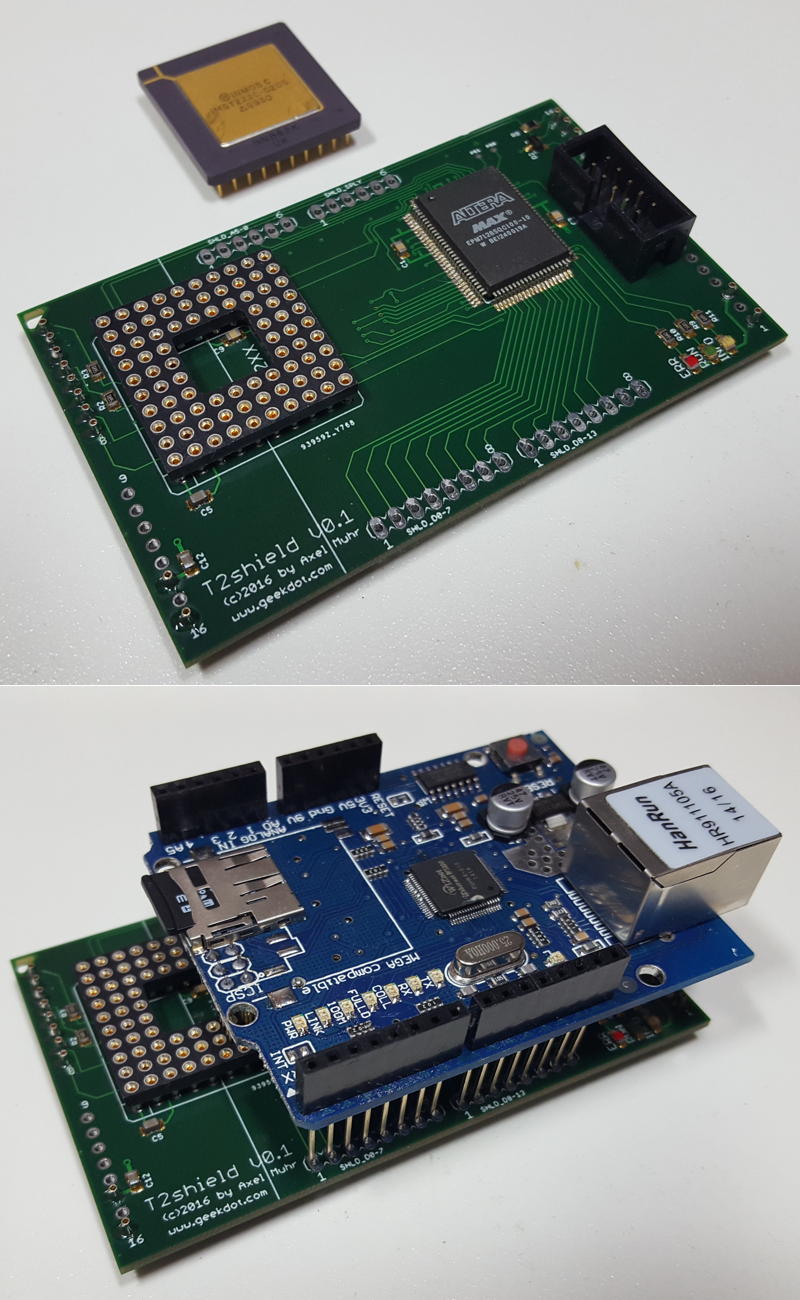
Without much further ado, here is the T2shield (v0.1) with a shield loosely put on top to get an idea…

t2shield

Arduino shields mainly use the SPI bus for data transfer. With its 10+Mbps SPI is much faster than e.g. I²C (which I used for my T2I2C TRAM) and can cope with fast(er) peripherals.
But this also ruled out a slow IMSC011/12 link-adapter design like the one used on the T2I2C. Also there’s no of-the-shelve SPI master controller to simply glue a bus to it.
So the design turned out much more advanced this time:

  • A 16bit Transputer (with 64KB SRAM) handles the high OS-link speeds as well as the ‘glue’ like File/Ethernet handling.
  • A comparably big CPLD (100pins, 128 marcocells) implements the SPI master controller as well as handles the T2xx memory- and interrupt-handling.
  • All Arduino digital-pins and nearly all analog-pins are connected to the CPLD to adjust to any available shield.

Also this new TRAM design is a “first” for me in many aspects:

  • 1st usage of a 16-bit T2xx Transputer (vs. 32bit)
  • 1st serious utilization of a CPLD (besides the baby-steps taken with the T2A2)
  • 1st Size-2 TRAM

Initial status

Transputer

[wppb progress =100 option=green] 100% done

A T222 Transputer is -after fixing some stupid errors- happily running and has control over his external RAM.
Here’s the first sign of life by RSPY (a brilliant ispy‘ish tool of Michael I really need to write a post about soon):

# Part rt Link0 Link1 Link2 Link3 RAM@cycle
0 T2   20 HOST  ...   ...   ...   4K@1,56K@2|

That means: A T2xx @ 20mbps linkspeed is connected to the host (PC) and has 4K internal and 56K external RAM… wait a second! just 56K? Yes, that’s because the internal 4K overlaps and RSPY leaves the up-most 4K untouched as most peripherals are mapped there and poking there could create unwanted effects…

CPLD

[wppb progress =10 option=yellow] 10% done

All basic Transputer controls are in place, LEDs are controlled by the CPLD

TODO: Implement the SPI master in VHDL. That’s THE biggest challenge for me being a total VHDL noob. Again, I wouldn’t got this far already without the tremendous help from Michael Brüstle, my VHDL Jedi-Master.

Drivers

[wppb progress =100 option=red] 0% done

Write the (Helios) driver to handle file and/or network access. This should be (optimistically) be compatible to existing file- or Ethernet ‘servers’. This will probably be the most time consuming task.

Progress?

This is (also) the first time I’m posting about a project which is not finished. So I will keep you posted about the progress with new posts in this “T2shield” chapter of this wonderful little page.
If you do own

  • a Transputer network
  • a free size-2 TRAM slot
  • a T2xx Transputer
  • some VHDL/Occam/Helios driver skills & knowledge

shoot me a mail and I might provide you a T2shield to join the development.

That said, here’s a first little sign of life:
The Transputer writes numbers to a mem-mapped address (0xFC00) while the CPLD reads the lowest 2 bits and displays them by 2 of the 3 LEDs on the T2shield

Updates for Apple OSes… but not what you think.

Yeah, iOS got an Update a couple of days ago… and so will Mac OS,  MacOS X, OS X, macOS in 4 days, making your 2010 Apple device obsolete (perfectly fitting in my last rant blog post). Boring… not the Apple OSes we’re looking for.

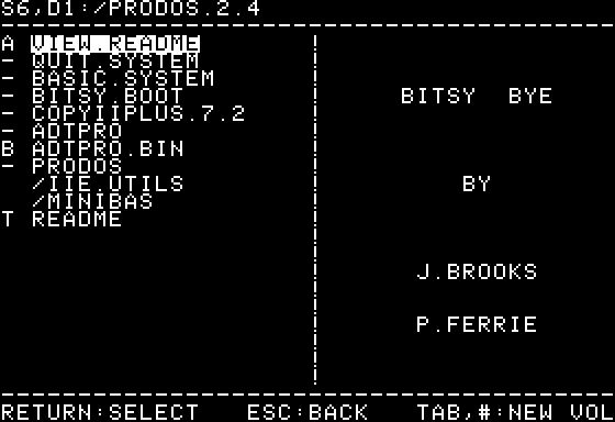
No, what I’m talking about is ProDOS just got updated to version 2.4! Yes, THAT ProDOS from  1983 running on Apple IIe computers.
Thanks to internet goddess, you can even play around with it in your browser.

prodos_2_4

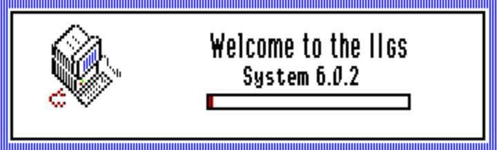
But not enough: After 22 years, 2 months, 2 days and 2 hours GS/OS got an update to V 6.0.2, too. That’s the System 6 look-alike OS running on the 8/16 bit Apple IIgs machine. By the way, one of my favorite Apples (also used in some of my projects).

welcometo602

That’s the spirit guys!

Weitek Abacus FPU

This is the first post on GeekDot about a single IC. While I did a lot of writing about ICs, mainly CPUs and FPUs, back in the BBS days (German) I stopped doing so after that and concentrated on collecting them during the following years – a true love never dies 😉
The Weitek Abacus FPUs were always special, exotic and unaffordable for the most of us. Today they additionally got a touch of a mythic being, especially as 386/486 boards featuring the special  WEITEK socket are dying out fast. Not mentioning the Abacus FPU itself.

Recently I had a mail conversation about the Abacuses and because they’re are memory mapped, I thought they might actually fit quite good into the range of my other accelerator post as the DSM860 or all those Transputer cards.

I wasn’t planning to go into all the details about the Abacus models 3167 and 4167 and went looking for a handy Wikipedia link.
To my surprise that article is pretty general and just briefly touches all product ever made by WEITEK.
So, the best source of technical information about these FPUs is the highly recommendable posting “copro16a.txt“, written by Norbert Juffa in 1994.
I’d call it the most comprehensive write-up about FPUs until that date. Because you’ll never know what happens to external links, here’s the (shortened) part about the Weitek chips:

The architecture of the Weitek chips differs significantly from the 80x87.
Strictly speaking, the Weitek Abacus 3167 and 4167 are not coprocessors in that they do not transparently extend the CPU architecture; rather, they could be described as highly-specialized, memory-mapped IO devices. But as the term "coprocessor" has been traditionally used for these chips, they will
be referred to as such here.

The Weitek coprocessors have a RISC-like architecture which has been tuned for maximum performance. Only a small instruction set has been implemented in the chip, but each instruction executes at a very high speed (usually only a few clock cycles each). [...] 
In contrast to the 80x87 family, the Weitek Abacus does not support a double extended format, has no built-in transcendental functions, and does not support denormals. The resources required to implement such features have instead been devoted to implement the basic arithmetic operations as fast as possible.

While the 80x87 coprocessors perform all internal calculations in double extended precision and therefore have about the same performance for single and double-precision calculations, the Weitek features explicit single and double-precision operations. For applications that require only single-precision operations, the Weitek can therefore provide very high performance, as single-precision operations are about twice as fast as their double-precision counterparts. Also, since the Weitek Abacus has more registers than the 80x87 coprocessors (31 versus 8), values can be kept in registers more often and have to be loaded from memory less frequently. This also leads to performance gains.
[...]

To the main CPU, the Weitek Abacus appears as a 64 KB block of memory starting at physical address 0C0000000h. Each address in this range corresponds to a coprocessor instruction. Accessing a specified memory location within this block with a MOV instruction causes the corresponding Weitek instruction to be executed. (The instructions have been cleverly assigned to memory locations in such a way that loads to consecutive coprocessor registers can make use of the 386/486 MOVS string instruction.)
This memory-mapped interface is much faster than the IO-oriented protocol that is used to couple the CPU to an 80287 or 80387 coprocessor. The Weitek's memory block can actually be assigned to any logical address using the MMU (memory management unit) in the 386/486's protected and virtual modes. This also means that the Weitek Abacus *cannot* be used in the real mode of those processors, since their physical starting address (0C0000000h) is not within the 1 MByte address range and the MMU is inoperable in real mode. However, DOS programs can make use of the Weitek by using a DOS extender or a memory manager (such as QEMM or EMM386) that runs in protected/virtual mode itself and can therefore map the Weitek's memory block to any desired location in the 1 MByte address range.

Typically the FS segment register is then set up to point to the Weitek's memory block. On the 80486, this technique has severe drawbacks, as using the FS: prefix takes an additional clock cycle, thereby nearly halving the performance of the 4167. Most DOS-based compilers exhibit this problem, so the only way around it is to code in assembly language.

Ok, so we have a good idea how the Abacuses work and how they can be used. … but what’s the story behind the company?

This is a ‘web found’ © by antiquetech.com
“Founded by Chi-Shin Wang, Edmund Sun, and Godfrey Fong (President and CEO) in 1981 in San Jose. All founders immigrated from China.
Weitek specialized in high-performance digital semiconductor components and systems for the computer and workstation industries. Weitek floating point units have been used with Inmos Transputers (Floating Point System T-series Hypercube, 1986), National Semiconductor NS32032’s (Encore Multimax, 1986), and Intel 386’s (1988). The 2048 was used in the Thinking Machines Corporations CM-2 Connection Machine. Weitek produced floating point processors for HP. HP allowed to Weitek to use it’s facilities to make chip for themselves and for their competition.”

When dramatically loosing ground to the 486DX2 Weitek moved away from the x86 platform and concentrated on SPARC CPU and FPUs as well as MIPS FPUs. That worked quite well for some time and in the 90s they finally moved into the frame buffer and graphics accelerator business. Their POWER P9000/P9100 models were quite successful but lost when players like S3 and ATI started to flex muscles.

Specs

So from our (PC-compatible) perspective there are two models of interest: The 3167 and the 4167. Basically they only differ in the bus protocol to either the Intel 386 or 486.
If you need more detailed data, I make the original specs available here for the 3167 and 4167 as PDF.
Both Abacuses clocked up to 33MHz. Especially the 4167-33MHz is very hard to find these days. That said, it might be possible to overclock a 25MHz version to 33MHz providing sufficient cooling. I found this press snippet where WEITEK proactively promoted overclocking a 33MHz to 50MHz by using a peltier element made by ICECAP – so when overclocking that by 51%, the 32% from 25 to 33MHz should be an issue:

WEITEK and ICECAP announce 33MHz version of Abacus 4167

Ram Ganapathi Mar 30 1992, 02:57 pm
WEITEK and ICECAP announce 33MHz version of Abacus 4167

Weitek Corporation and ICECAP Technologies announced today that users of 50MHz Intel 80486-based personal computers can realize a 50% performance increase for numeric-intensive applications by combining the 33 MHz version of Weitek’s Abacus 4167 math coprocessor with the ICECAP thermal management device. Superior system performance is achieved without degrading system reliability.

Using it

Applications that took advantage of the Weitek Abacus were scarce. AutoShade, Autodesk Renderman, 3-D Studio were the most prominent to use a Weitek coprocessor.
If you happen to own one, you might actually use or at least test it… so here’s the official test-suite from Weitek. It contains these tools

  • DOS TSR to update the BIOS for Abacus support (if missing)
  • A test tool wich checks for an Abacus presence using INT 11h BIOS calls.
  • A diagnose tool
  • 2 demos: A side-by-side Mandelbrot benchmark (yay!) and rendering a phong shaded beach ball
  • Abacus macros for using it natively in your cool assembly code

When I find the time to pull out my Weitek-PC, I’ll post pictures of the demos… feel free to comment if you feel I’ve been missing out something.

The PPC Parsytecs

Well, because I’ve been asked every now and then… I’ll briefly touch the “Post-Transputer era” of Parsytec and thier PPC products in this Post.
No, I don’t own any of those, and they only run/ran Parsytecs very own PARIX OS, so I’m not of much help when it comes to revive your system.  As often said, I don’t like to see Transputers being degraded to communication processors. So this is just for completeness and might help to identify your brand new dumpster-dive finding:

The missing link: PowerTRAM 601

These are the only Parsytec products which truly and directly bridge ‘old-world tech’ (i.e. INMOS) with ‘new-world tech’.
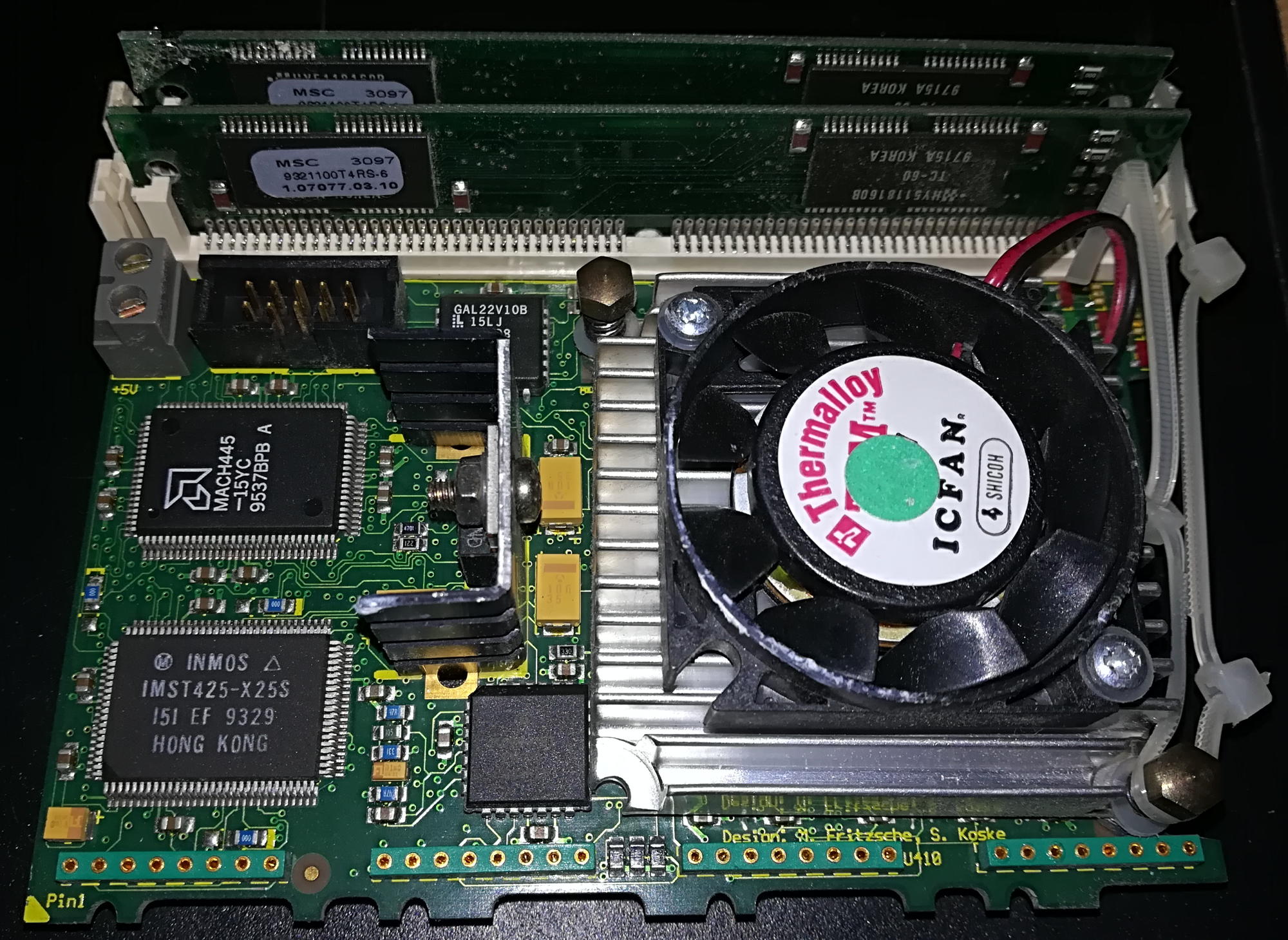
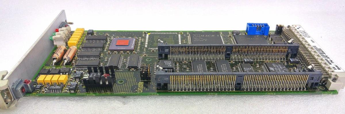
The PowerTRAM – available from 1994 to ca. 1996 – was a size-4 TRAM featuring an 80MHz 601 PowerPC which is memory-mapped into a 25Mhz T425 memory.

The Front has all the glamour. In the lower left corner you can spot the T425 in a QFP package, above it is a MACH FPGA most likely containing the glue logic.
The remaining space is used by the mighty PPC601 hidden under a huge heat-sink and a fan (the 80MHz version was the fastest 601 fabricated using a 0.6 µm CMOS process and ran quite hot) as well as two PS/2 SIMM slots for its RAM.


[Pictures courtesy by J. Snowdon]

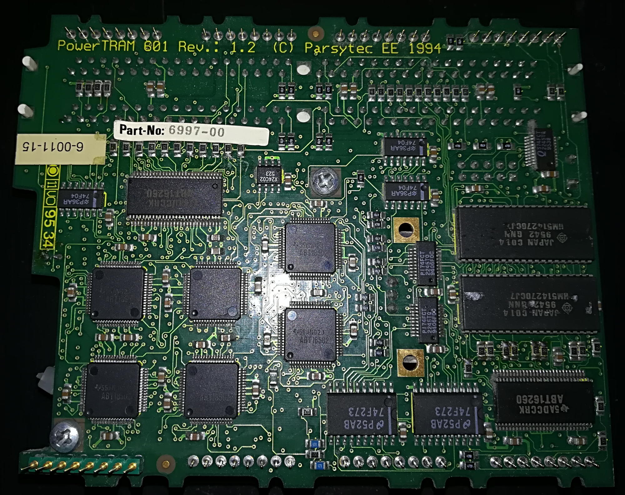
The rightmost third of backside is populated with 1MB of RAM for the Transputer and the classic logic to connect it (mainly latches).
The left two thirds are used up by quite some transceivers. Namely six ABT1852 18-bit bus transceivers (the square ones) which most likely connect the Transputer and PPC busses as well as covert the latter 3.6V level to the the T425 5 volts.

The “other x’plorer”

Well, yes, there was another x’plorer in existence. As with the GC-system, Parsytec later offered the “PowerXplorer”- you may guessed it already: It used the cluster from the PPC601 powered GC systems.
Interestingly enough there seem to be 2 versions in existence. At least the German computer magazine c’t reported in May 1994 that there’s a 2 CPU and a 4 CPU PowerXplorer… and featured the two below images as a proof.
Maybe the 2-CPU model was a beta-model or even using early PPC604’s? At least it features SIMM sockets vs. the soldered RAM used in the 4 CPU version.

   p_xplorer4cpup_xplorer2cpu

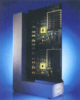
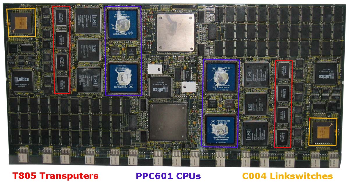
If you’re really-really interested in that model, here’s a big (Click to zoom) picture of the PPC cluster board. I’ve marked the important parts for easier finding.

powerXplorerBoard

TPM-MPC

The TPM-MPC  (Transputer Processing Module – Multi Processing Card) is basically a single CPU version of the PowerXplorer. So one T425 is handling the link communications and, depending on the revision, a 100, 133 or 200MHz 604e PPC is doing the number-crunching.

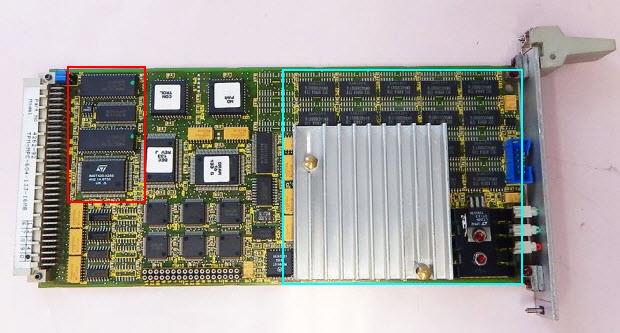
This is a Revision 1 TMP, far left in red frame you can spot a T800 Transputer with its RAM – in the green frame is the PPC604 and soldered 16MB of EDO RAM:

TPM_rev1

A somewhat different version (can’t spot a Rev making) providing 32MB RAM to a 100MHz PPC604 and having the glue-logic between the 2 CPUs shuffled around a bit compared to the previous version:

TPM_rev1_5

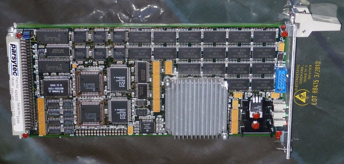
The Rev.2 model features SIMM sockets for the EDO RAM and has a slightly different layout.

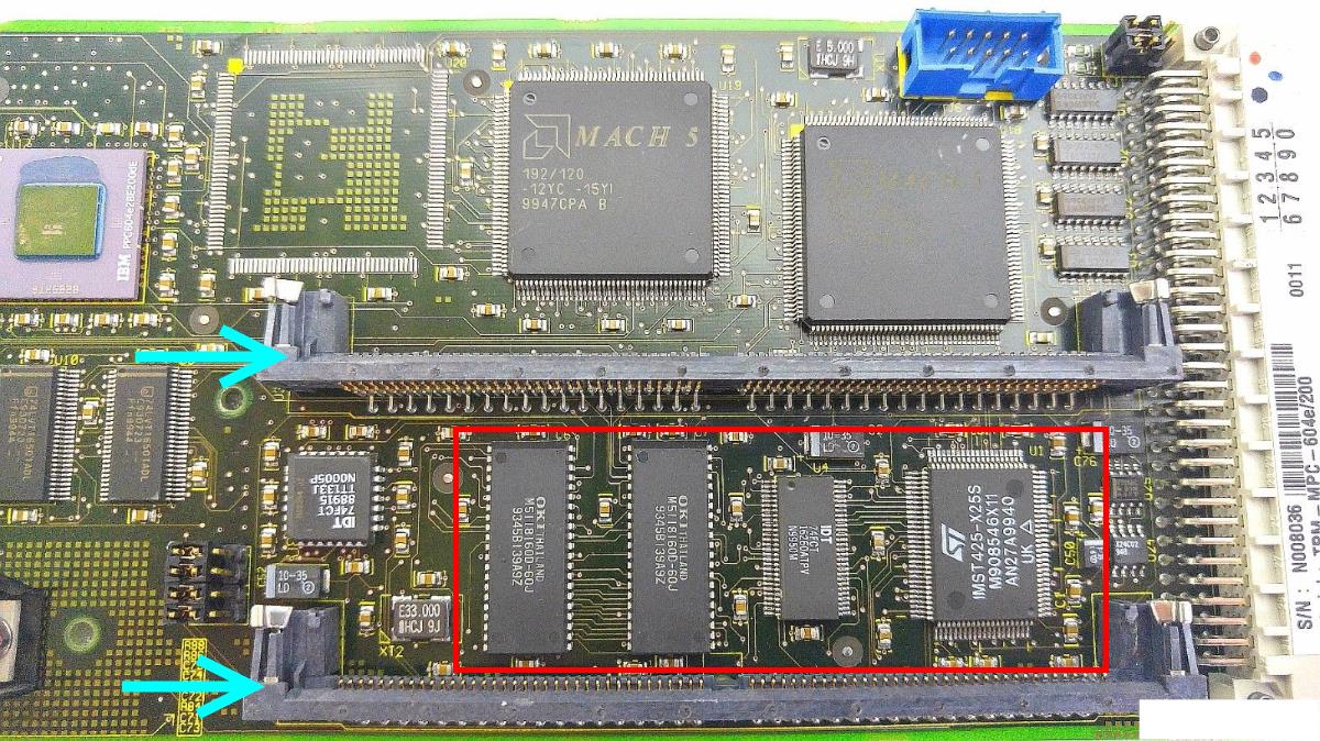
TPM-MPC_total

The Transputer part on this one is a T425 (who needs a FPU for just doing data-shifting?!) with 1MB RAM, framed in red between the 2 SIMM sockets, marked with blue arrows:

TPM-MPC_right

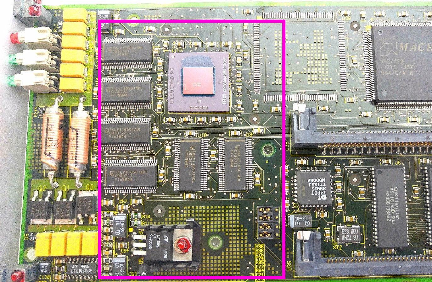
The PPC side (heatsink removed) including some drivers and the 3.3V supply.

TPM-MPC_left

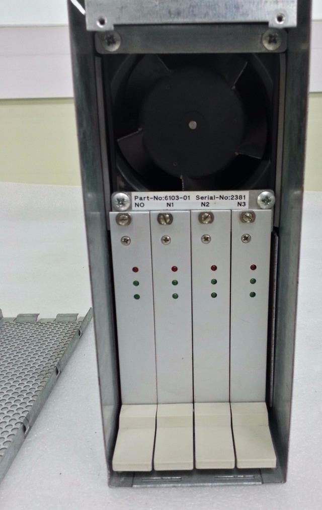
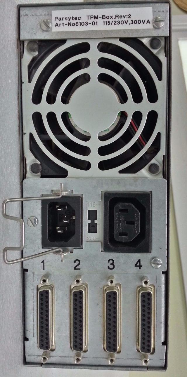
Independent of the revision, TPMs went into a TPM-Box. A simple, steel box with a power-supply, two fans and a backplane for 4 TPMs. This is it from the front (grille removed):

TPM_box_front

…and the even less impressive back.

TPM_box_back

As some ePay auctions mention “taken from RVSI 5700 SYSTEM” I assume the main usage for TPMs were optical analysis/inspection systems which Parsytec built when turning their backs to super-computing.

Finally silence

Working a lot with my Blade 150 called “Sparky2” recently, the CPU fan turned out to be too loud, still. So I dug deeper into the matter and it turned out easier than I thought…

SUN -for whatever reason- decided to put a comparably small 40x40mm fan on top of the non-standard heatsink and additionally placed some aluminum spacer around it.
Removing everything revealed a totally standard PGA 370 socket! That’s Pentium III, if you remember… So a quick check in my old-junk-stash resulted in 3 nice heatsinks. I took the full-copper one and mounted a 60x60mm fan on top.
Put everything into place – done (BTW: SUN didn’t use any thermal grease, so did I)… but the bigger fan was still too noisy at 12 volts  🙄

After checking the fan also starts at 5 volts, the decision was clear: Bigger, massive copper heatsink plus bigger fan should be sufficient at lower revs.
There’s no direct 5V source on the Blade 150 motherboard. So I chose the vacant connector for the optional 2nd hard-drive (the closer floppy connector would do, too – but I had no spare cable to salvage).

Simply connecting the fan there wasn’t enough. OpenBoot actually checks for the fan tachometer signal and refrains from booting the system without one connected.
I was already evaluating how to build a signal dummy (a simple 555 timer circuit) when I decided to check if a simple forking out of the signal is enough. So I used a 2-wire cable and put ground and the tachometer signal to the on-board fan connector… and voilá that made the OpenBoot happy. Finally silence!

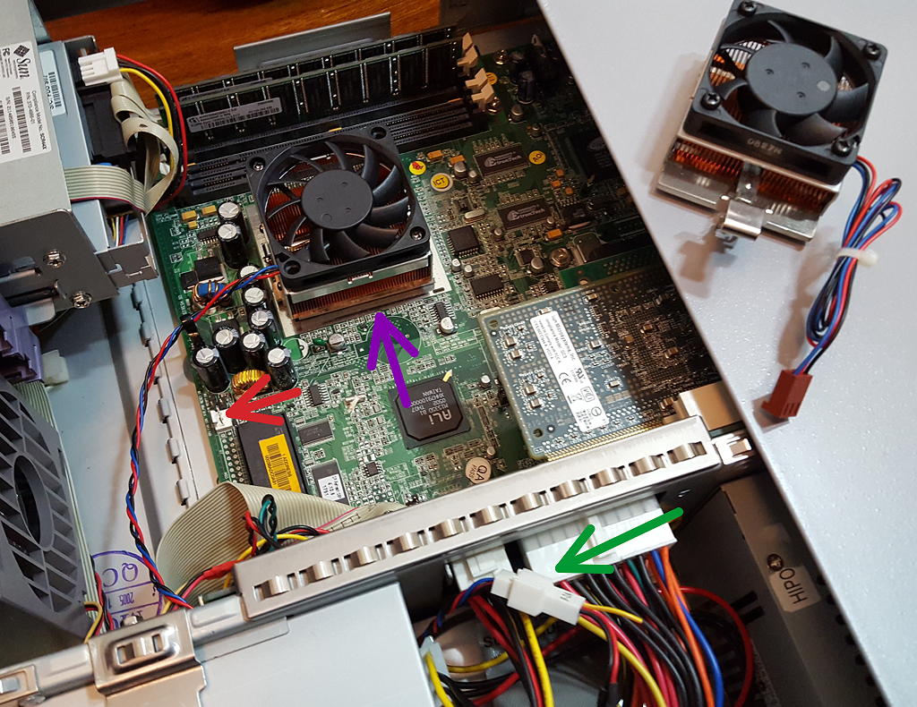
Here’s a piccy.

  • Purple arrow: The new & bigger heatsink (the old on lies on to of the case, so it looks bigger than it actually is)
  • Red arrow: The original fan connector (it still misses the tachometer signal bypass in this photo)
  • Green arrow: This is where the new fan is connected.

Blade150_cpu_fan

Feb-May Updates

Again, some posts/projects received silent updates worth mentioning:

Inmos B008

Introduced at the sunset of the Transputer era, the INMOS B008 was the successor of the B004 of which it dramatically differed:

  • 16-bit ISA connector (for Interrupts/DMA, it’s still an 8 bit data path)
  • 10 TRAM slots
  • C004 and T2xx on board

The usual source provides the full manual/documentation… down to the GAL equations.
All these enhancements enabled the B008 to create simple, yet powerful Transputer networks on a single expansion card and still makes it the perfect platform for todays Transputer retro experiments/fiddlings.

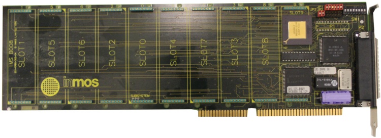
Here’s a late “Rev.F” version of the IMSB008:

IMSB008E

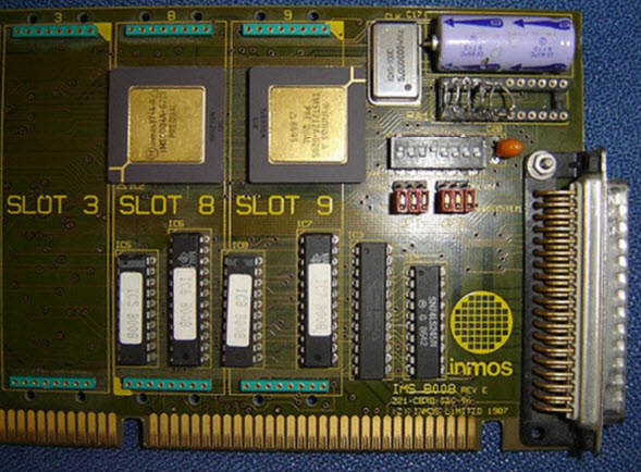
The previous revision E had a ceramic version of the T2xx and used GALs instead of the CPLD you can stop in aboves picture.

B008_revE

Clones

Obviously the Inmos B008 had clones as the B004 did.

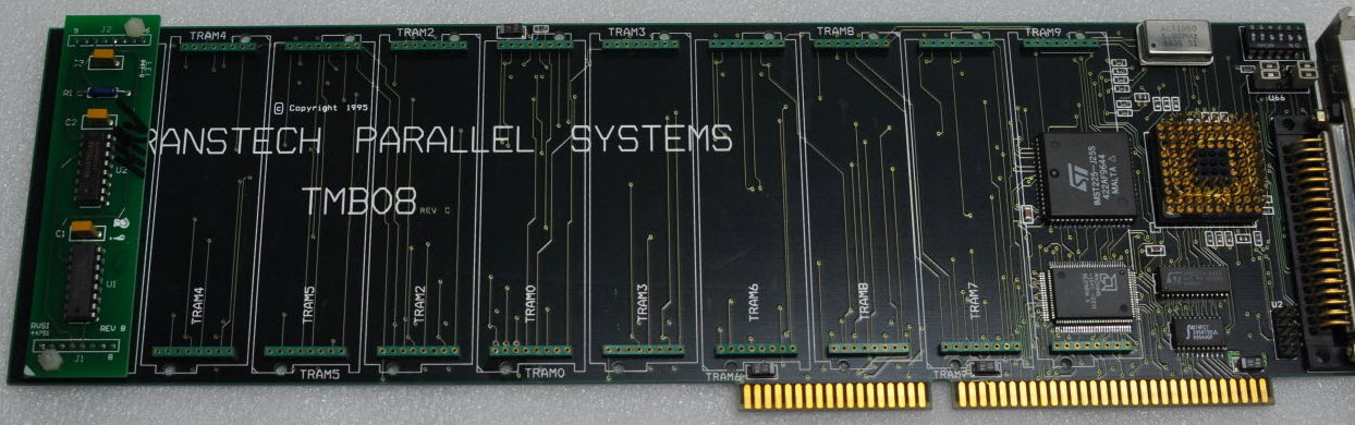
Transtech TMB08

Well, I guess there’s nothing which Transtech did not clone and/or improve…
In this case they used a AMD MACH CPLD from the beginning, a PLCC version of the T225 and everything else was SMD.

TMB08

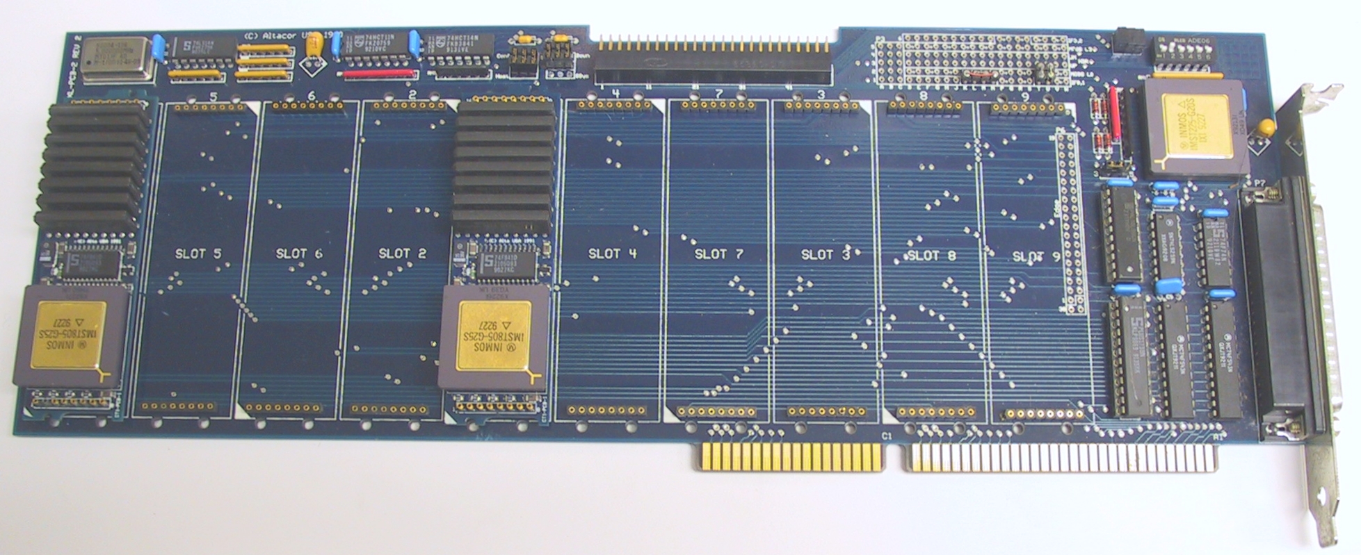
Alta SuperLink/XL Transputer PC Card

Alta Technology was a spin-off of Computer System Architects (CSA).
The SuperLink/XL board used TRAM modules like the Inmos B008, but featured a 20 MHz IMST225 Transputer to handle external interfacing and a beefed-up host interface design. Like the B008 it supported 10 TRAM’s

Altacor SuperLink XL

ARADEX

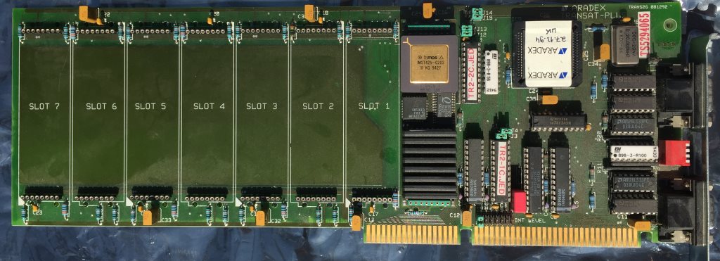
One of my first TRAMs was an ARADEX one, so this is a first for me, too. Actually I wasn’t aware that ARADEX also made TRAM carriers… but they seem to do quite some:

TransAT Plus

Their interpretation of the B008 theme features just 8 TRAM slots (vs. the 10 “standard”) which are strangely enough sorted in ascending order (0-7) and not like the B008 order of 1, 5, 6, 2, 0, 4, 7, 3, 8, 9. Also the TransAT provides two 9pin D-subminiature connectors in contrast to the B008s 37pin connector – most likely its layout is the so called Aalener Link-Interface. That includes the RS-422 differential drivers and receivers next to the connector (AM26LS23’s and AM26LS33’s).

Concerning other parts, besides an C012 they used some sort of CPLD – presumably to control the 16 bit bus – in the photos I have, I can clearly see the traces coming form the ISA Bus’ D[8-15].
It also uses the IRQs 10-12.

Last fun bit: They named the two GALs with their JED filenames. Very handy 😉

aradex_transat-plus

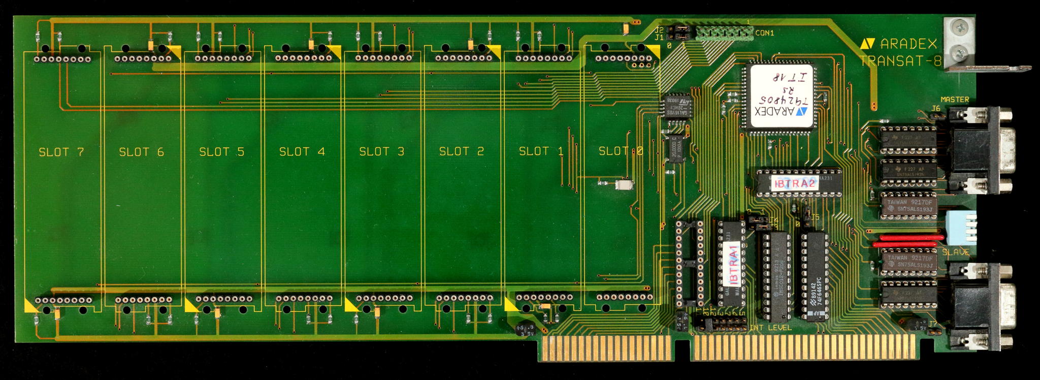
TransAT-8

The “8” in its name makes it a valid member of this collection – but it misses an C004 and also has just 8 TRAM slots… so maybe it should be considered somewhere between an IMSB004 and B008?

This time TIs 74ALS192/193 differential drivers are used, the PLCC chip is yet unknown… and in this case, a TTL chip (next to the ISA slot) is missing… all in all, it looks like a refresh of the TransAT Plus to me.

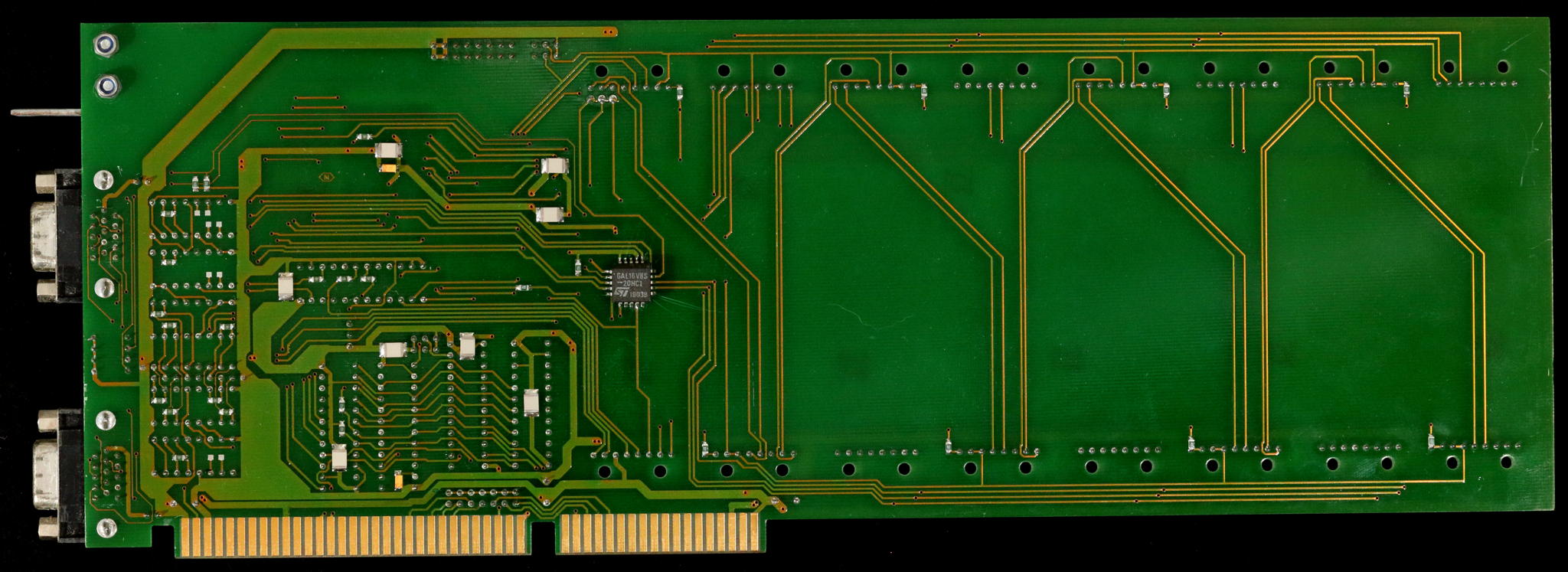
I even have a piccy of the back-side. Why the heck is somebody putting a GAL there?