Tag Archives: ISA

The STG[A]TW

This is my first ever project I did for one of my favorite computers, the ATARI Mega-ST. Like told in one of my blog posts, the ATARI ST was my 2nd greatest love ❤ (after the C64) and being part of a very  cool company back in the days I only have fond and happy memories of it.

After all the years of fiddling with nearly every machine on the market, it’s like coming home by just looking at its system font or hearing it’s specific bell-sound (even the ever-annoying key-click sound it makes by default).
And now it’s time to do something cool with it… adding, what I’ve missed back then: Color and -of course- Transputers 😉

TLDR;

Ok, so you’re in a hurry or suffer from severe ADHD?

This is a graphics card for the ATARI Mega ST internal bus including a Transputer interface.

Got it. More details please…
What about software? (links to a different post)
Why, for god’s sake!?
There’s a relocator, too?

Ok, how much?

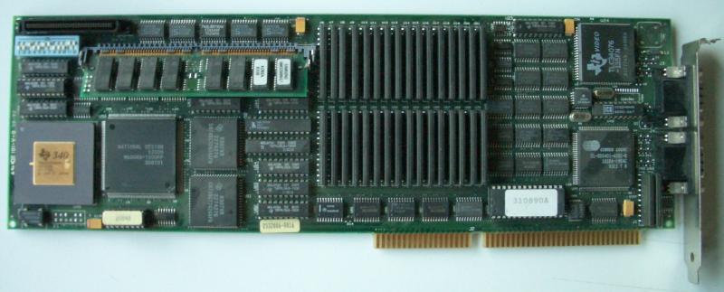
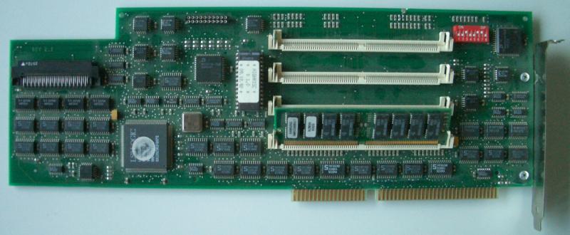
Say hello to the STG[A]TW!

What’s that about the strange naming?! Well, this card is a hybrid of a classic STGA ISA graphics-card adapter and a Transputer interface for the Mega-ST bus.
Mega-ST, high-res graphics and Transputers? Mhh, does this ring a bell? Yes, component-wise this is exactly the configuration of an ATARI ATW800, the famous and rare ATARI Transputer Workstation (for which I designed a Farmcard, just in case you own an ATW).
So adding the two, it’s an STGA-ATW or STG[A]TW for short… and it looks like this:

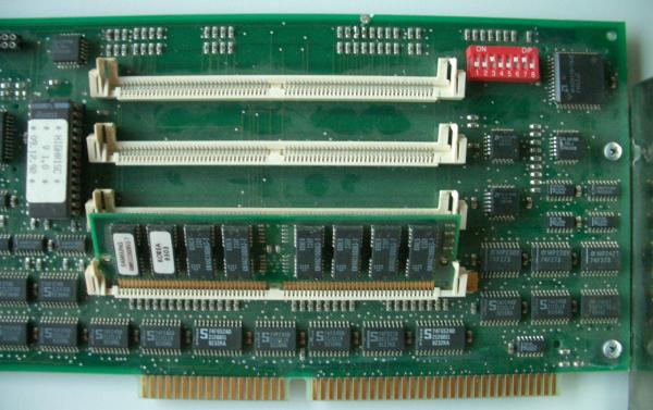
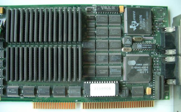
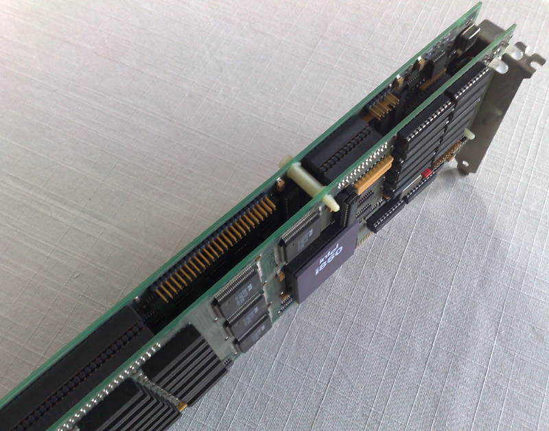
Looking at the top you’ll spot the 90° angled ISA Slot at the right edge, giving (selected) ET4000 graphic cards a home.
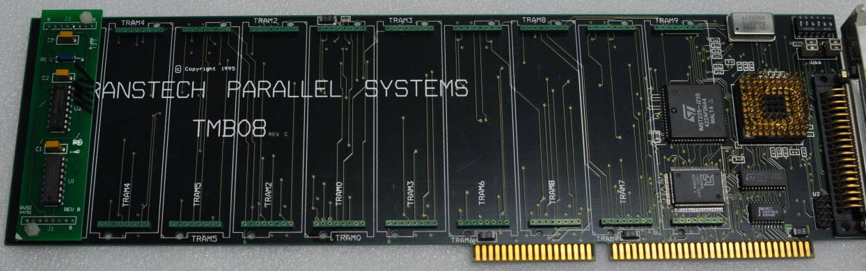
To the left there are two Transputer TRAM slots making it possible to use two size-1 or a single size-2 TRAM.
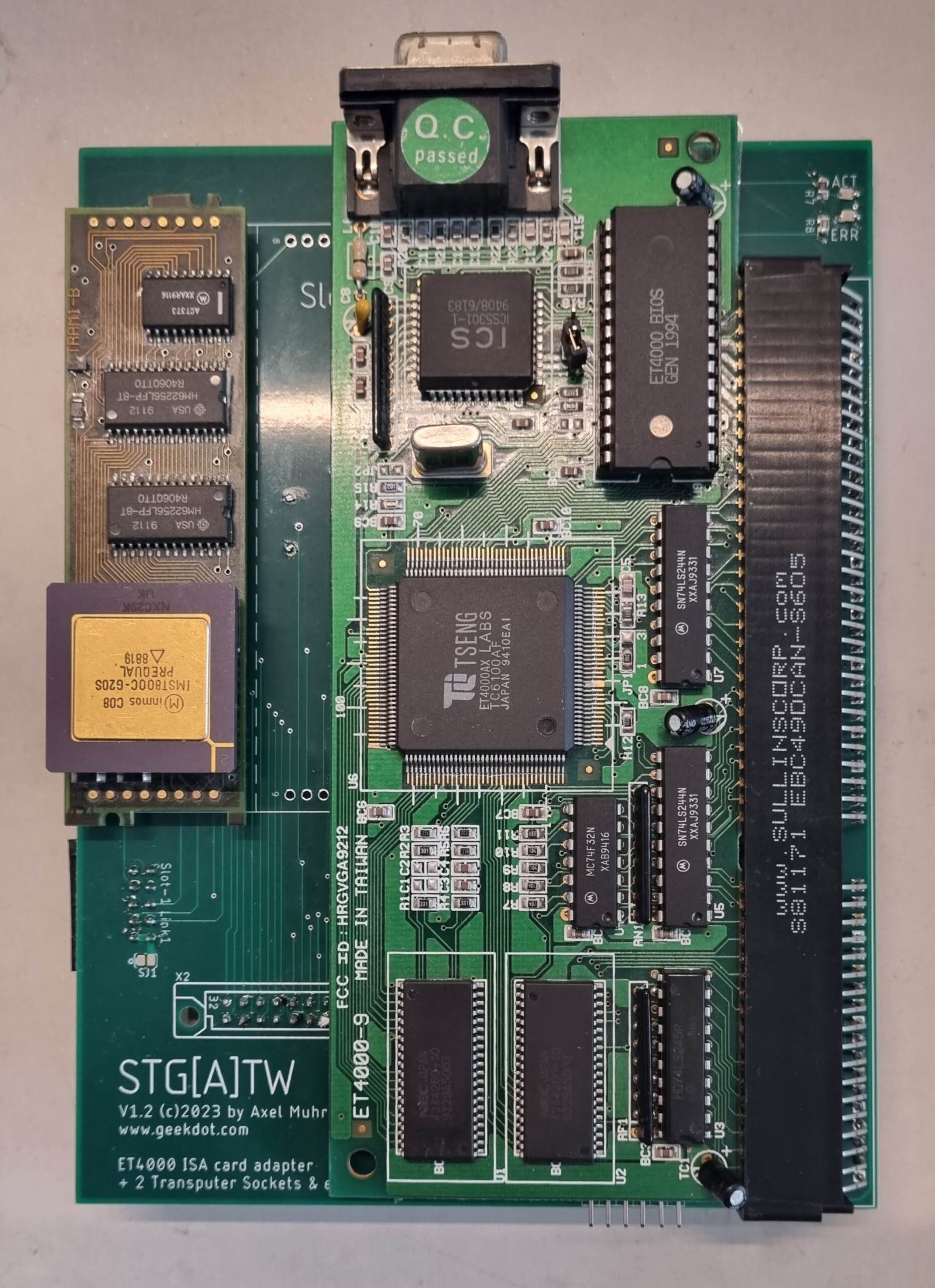
Obviously, an ISA card and the TRAMs would collide, so you have to choose… or you’re a lucky owner of a low-profile ET4000. Then you could use your VGA card plus one TRAM like this:

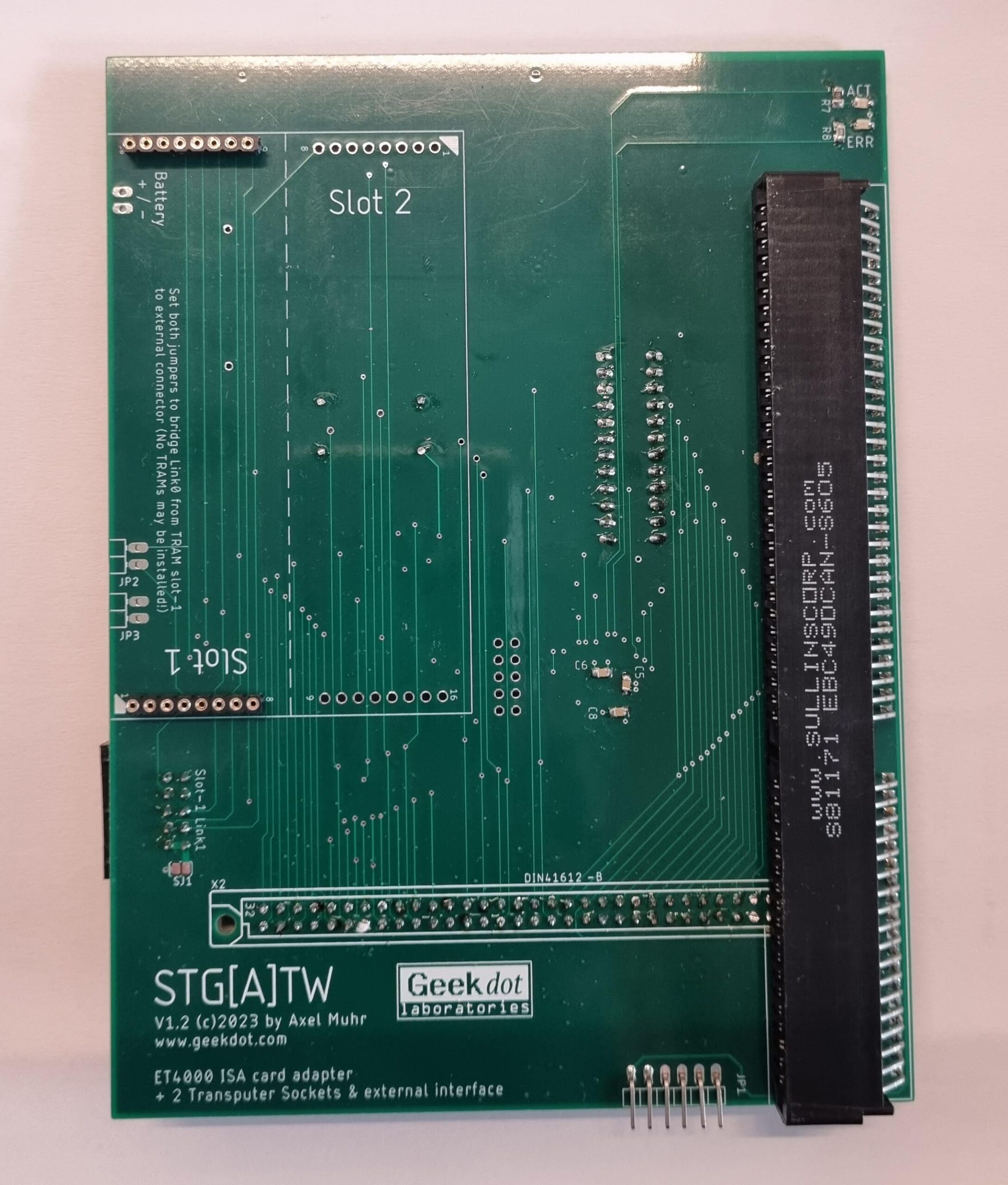
But even if your ET4000 card is covering the whole STG[A]TW don’t despair! Looking at the backside you can spot the external Transputer link connector (on the right edge):

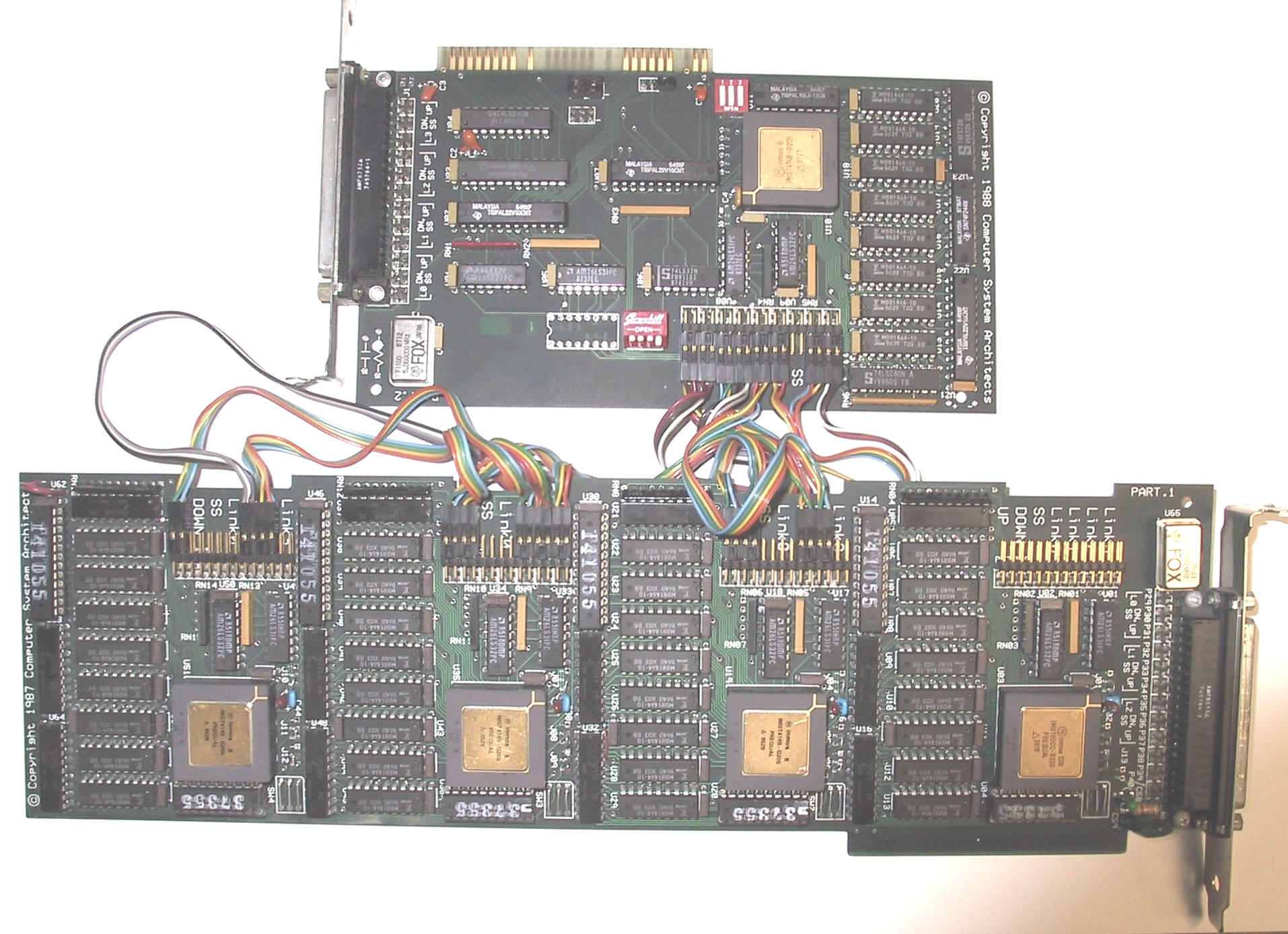
Using this you can connect to e.g. an external Transputer(-farm) of any size… for example something like my 64 CPU Final Cube 🔥

Looking further around the backside you can spot a preparation for a CR2032 coin-shape battery holder. That is meant to replace the two AA batteries used in the original case-lid because depending on the TRAMs used, it might be necessary to remove the battery compartment (yes, you’d need to cut it out 😰) .

Talking about power… at the bottom you can see the external power connector which supply is mandatory – you need to connect at least 5V and ground, optionally 12V if your ET4000 needs that.
That said, I highly recommend to make sure your Mega ST’s PSU is powerful enough – best would be to replace it by e.g. a Maxwell RD-50A.

Why?!

I knew you’d ask. Well in case you haven’t noticed yet, I’m a total Transputer nut. It’s a fabulous, genius CPU and design. The more you dig into it, the more you’ll love it.

Back then I adored the ATW800 and always wanted to own one. But it was insanely expensive and -to be honest – wasn’t a real member auf the ST/TT-family anyhow.
This is because the Mega-ST1 inside the ATW was mainly used as a bootup machine for the Transputer and after that was up and running, everything the ST did was file- and user-I/O (Mouse, Keyboard, RS232).

In my humble opinion, the STG[A]TW is (somewhat) the way how ATARI should have done it back then. Instead of creating an ‘island solution’ they should have used the existing install-base and offer an expansion to it. Plug in the missing parts (graphics & Transputer) and keep the TOS/GEM eco-system in charge.
Users could keep running their applications and use the extra ‘ooomph’ to speed them up. Think of all the accelerators Apple Macintosh users had available to speed up PhotoShop filters or have it do the heavy number crunching of science applications etc.
Even all data has to travel over the bus to the Transputer and back, this is still faster than the 8MHz 68000.

Given that in 1990 about 350 ATW800 were produced and sold at 5000-7000 GBP which equaled to about 13700 DM or 8000$ (that’s about 11400 GBP, 13700 EUR or the same in US$ today),
I bet the number of a “ATW for the poor” would have been much higher.

So, again, why? Well to have Mandelbrot fractals calculated fast and  in colo(u)r, of course!
Fast means ~60sec, even using slow GEM routines. Using the same algorithm and iteration depth, the ST’s 8MHz 68000 took nearly 3 hours to calculate the same fractal.

Here’s a quick peek how ‘fast’ looks like:

Evolution – a quick excursion

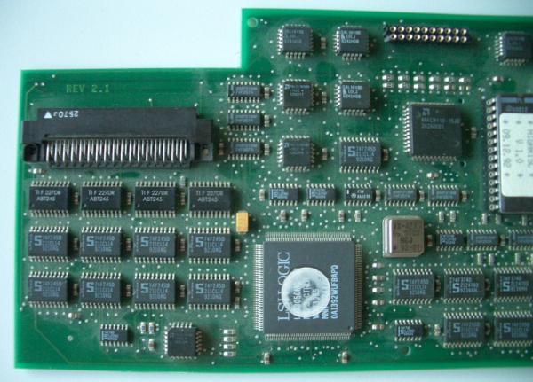
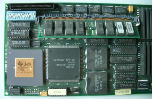
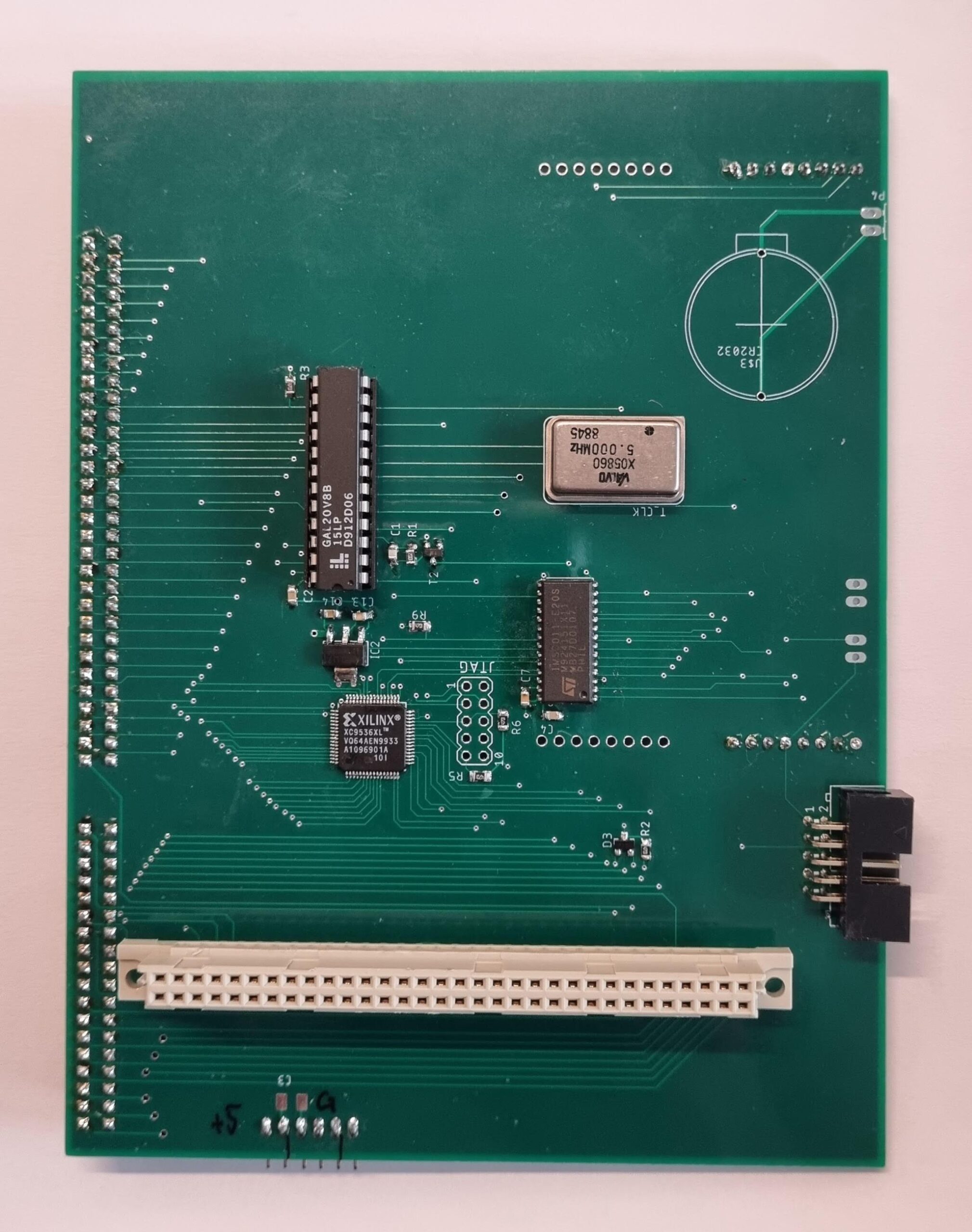
If you’re into hardware development you might wonder why there’s a very vintage GAL and a semi-vintage CPLD used in this design.
Here’s my explanation and shameful justification 😉

From the very simple and basic design of the STGA I took the usual nerdy feature-creep road to hell 🙄
My initial design naturally included the GALs logic into one big CPLD. And having all address-lines available on this, that design also included (on top of the ISA and Transputer interface) a 68882 FPU, an IDE interface and a ROM decoder… everything worked fine BUT all ‘modern’ ET4000 cards didn’t.
I stared at logic-analyzer traces for weeks and weeks and compared them to the original STGA they were absolutely identical. But whatever I did, I wasn’t able to get ET4k cards with a Rev. TC6100AF chip working.
In the end I decided to keep the STGA part as-is, including the external AND-ing of /LDS & /UDS and inverting of /DTACK and put the Transputer handing into a smaller (and cheaper) CPLD.
Thus the FPU, IDE and ROM decoding was off the table and to be honest, there are other solutions which do that job better anyhow.

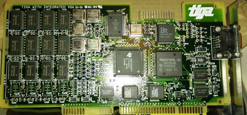
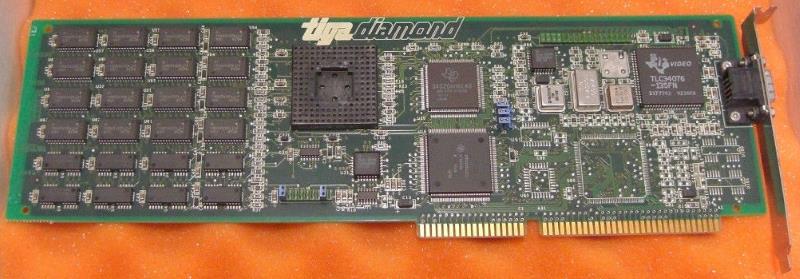
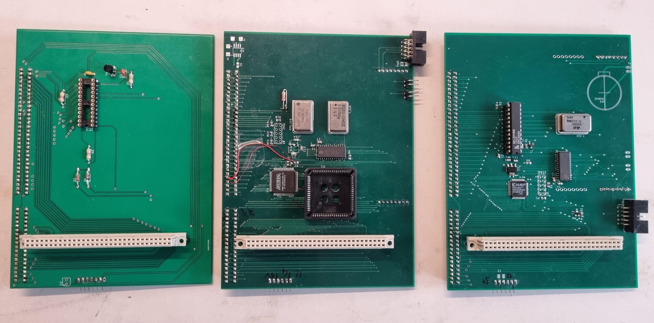
From left to right: STGA, the Über-STGA and the final STG[A]TW

So there you have it: Colorful high-res GEM combined with the mighty Transputer power… but I understand, that those low-profile ET4k cards are getting rarer and rarer and not everybody has an external Transputer farm to connect to.
So I made another card or better a so-called CPU relocator…

The TRAM-Relocator

Most (Mega) ST users out there already have one or more expansions to their system, mostly plugging into or onto the CPU creating a ‘stack’ of PCBs.
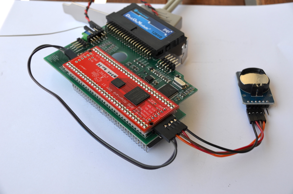
Because the STGA (as well as the STG[A]TW) overlaps over the Mega STs CPU socket you might want relocate the CPU a bit away from the Mega-Bus socket. Simple relocators simply move it a bit towards the front of the case. But that still results in having a stack of multiple extensions. For example here’s a Storm ST (Alt-RAM) on top of a Cloudy (4x ROM) plugged into a Lightning ST (IDE & USB):

This can get tricky in some crowded Mega ST cases…

I really liked the ‘Bus I/O port design’ of the Exxos’ STF Remake Project having multiple sockets next to each other.
And if you have your original TOS ROMs removed (and replaced by e.g. a Cloudy) there’s actually some space to roll out 4 of them having the Relocator sitting flush on the Mega-ST mainboard (make sure the backside of the Relocator is completely isolated!):

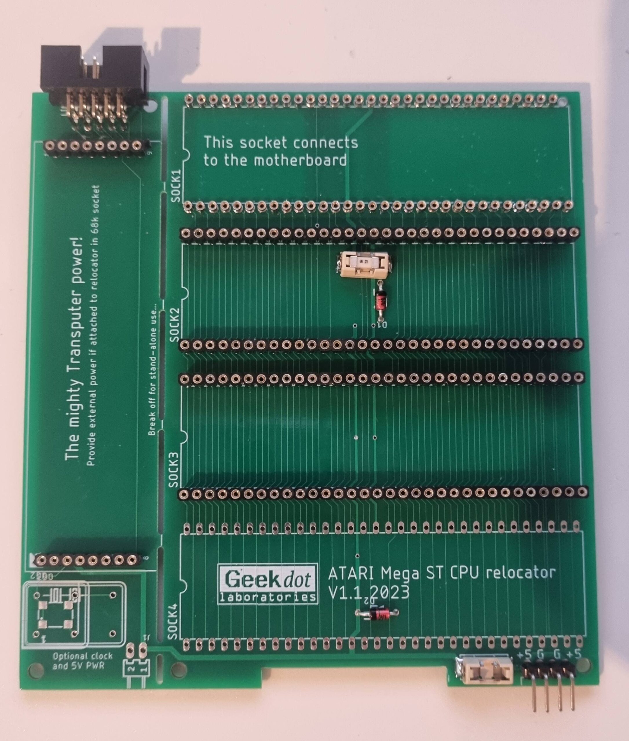
4 Sockets and a cool TRAM socket 😁

Like clearly written on the PCB, SOCK1 goes into the (to-be-retrofitted) CPU Socket and using ‘hollow pins’, it can take a CPU itself.

SOCK2-4 are available to extensions of your choice – all 3 of them are protected against power-surges by a fuse and a diode.
This design decision has been made due to my own painful experience loosing everything which had been plugged into the CPU socket… and the Blitter 😥

In the lower right corner are pins for an additional external power connector, also protected. That might be necessary depending what you’re plugging into those sockets.

Finally, the left edge is a Transputer TRAM socket which can be connected to the STG[A]TW by a 10pin flat-cable providing link signals and a 5MHz clock signal.
That way, you can use the STG[A]TW with an internal Transputer even your ET4000 card is big as a baking-tray.
It is highly recommended to use external power when doing so. The poor 68000 power-pins won’t be enough for it.

If needed, the whole TRAM part can be snapped-off from the Relocator to, uhm, relocate the TRAM elsewhere in- or outside the case or use it stand-alone. For that matter itself features an optional connector for power as well as a place to solder a required 5MHz oscillator and 2 mounting holes.

With everything in place, your “ATW800 for the poor” could look like this:

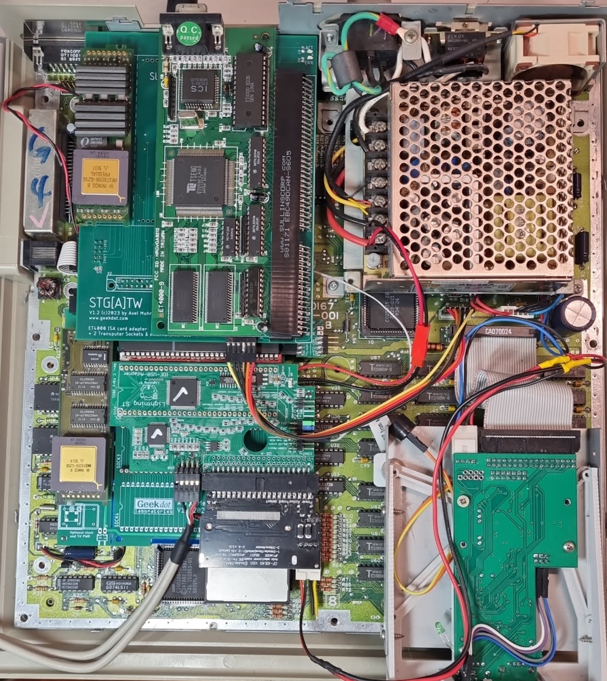
What you see here is the STG[A]TW plugged in, giving home to a low-profile ET4000 and a Size-1 TRAM.
The Relocator was plugged into the CPU socket and in its 1st slot the  Cloudy-Storm  and the 68000 sitting on top of it, took seat.
Slot 2 of the Relocator is taken by a Lightning-ST… and last but not least, a second TRAM was put onto the Relocator (you can spot the grey flat-cable connecting it to the STG[A]TW.

Want one?

All this sounds so cool that you want to own a STG[A]TW?
Well, first check out this list:

  • There’s next to no GEM user software for it yet
    👉 but we’re working on it and there’s a pretty good system support in place already – and Helios is running already! 🥳
    An extra post on that is currently in the works available here.
  • Do you have an ET4000 card of which you know it’s working with the NOVA drivers?
    👉 I am not able to support you in getting your specific card working – there are just too many models and permutations of possible TOS/GEM/Driver installations. See this atari-forum.com thread to get an idea…
  • Do you own a TRAM?
    👉 I might provide you with one at extra cost, mail me.
  • Do you have time to wait?
    I’m manually building these boards and it’s a lot of work (0.5pich SMD, lots of trough-hole pins to cut and file down etc.)

If that’s 4  times “Yes” I can build & sell you one of the 6 which I have left for 100€ (plus shipping)… yes, that’s hefty but the quite large PCB is 4 layers (for stable power-distribution), just the ISA slot connector is 10€ already, Mega Bus 5€, GAL, CPLD etc.etc…. plus, as said,  it takes quite some time to build & test them.
Drop me a mail on the bottom of that page if interested…

SOLD OUT… sorry 😥

As for the CPU-relocator, I’m selling un-populated PCBs for 8€ (Or get the gerbers here and have yours made at your favorite PCB manufacturer).
I’m not building them because the CPU ‘socket’ (SOCK1) is made of 64 single pins which you have to pry/get out of precision pin-headers.

That’s a tedious work you most likely want to do once… but not many times.

All that said – If you weren’t able to get a STG[A]TW, don’t despair.
I consider this as my stepping stone and learning platform for something cooler to come 😎.
Because I don’t like vapor-ware and hot-air-talking, I’ll tell you more when it’s a) done and b) working.

Digging deeper into the highRISC

After 7 years mainly doing research on Transputers and the i860, I had the feeling it’s time to do some more digging into the highRISC card.
If you have read my initial post about the miroHIGHRISC (and the Tiger) you remember the undocumented 20pin socket on the card (pictured in the upper right corner):

HighRiscLeft

Let’s have another look at the “UART port” again:

The pinout (the connector is rotated 90° counter clock-wise):

GND  oo  /WR0
D0   oo  INT2
D1   oo  /RD
D2   oo  /IOSEL
D3   oo  RESET (most likely)
D4   oo  A2
D5   oo  A3
D6   oo  A4
D7   oo  A5
VCC  oo  A23

Reading a bit of the BIOS’ disassembly, I stumbled across routines to talk to an UART.  A very common (D)UART of those days was the SCN2681. If you take a look at this chips specs, they perfectly fit to the signals provided at the HIGRISCs UART-port!

Here’s its pinout with the corresponding pins marked:


A2-A5 are used for A0-A3 on the 2681 and the only pin not directly represented is A23 which might be used to decode. Also, it nicely reveals that CPU INT2 is used for the UART.

The LR33000 datasheet tells me that there’s an 4MB IO-area starting at 0x1E000000 reaching up to 0x1EFFFFFF- most likely the 2681 will live there… and the corresponding signal called /IOSEL is available on the UART-port (and will perfectly help as chip-select decoder). Tadaa!

So after the UART we need to get the RX/TX signals to a higher level, i.e. the +/-15V of RS232 – this is the call for our old friend MAX232.

[current bread-board experiments sadly didn’t yield into ‘instant success(tm)’… I’m missing out something – need more time to investigate]

Bootcode / BIOS

The LR330xx CPU also has an /EPSEL EPROM select signal, indicating it’s accessing an EPROM expected to start at 0x1F000000 and ends at 0x1FFFFFFF (4MB right below the IO-area).
Using this knowledge and knowing that the MIPS standard boot-vector is at 0x1FC00000, it’s easy to feed the ROM-dump I did some years ago into the disassembler with the correct start address to do his job.

We need to get an understanding of this bootcode first, so that we can get an idea of “what is where” (e.g. ISA bus, UART etc) and later upload our own code and use those addresses.
Just to stick my head a bit into the clouds, the aim is to first port a then common MIPS monitor-program called ‘PMON’ and use that to run some sort of μLinux. But that’s probably another handful of years ahead…
PMON was a good source of information, because it’s originally written by LSI, supporting all the LSI eval-boards. Lo and behold, some of them had a 2681 UART, too… located at 0xBE000000, which is extensively used in my BIOS disassembly  😉
I have a certain feeling that miro borrowed some design ideas from the LSI Pocket Rocket evaluation board (don’t Google it, it’s a mythic being – if you have documentation, mail me!).

So this is the 2681 memory-map then:

#define BASE_2681 0xbe000000
#define SRA_2681 ((1*4)+BASE_2681) // 0xbe000004 status register 
#define THRA_2681 ((3*4)+BASE_2681) // 0xbe00000C Rx/Tx holding register 
#define ACR_2681 ((4*4)+BASE_2681) // 0xbe000010 Aux contrl. register 
#define ISR_2681 ((5*4)+BASE_2681) // 0xbe000014 interrupt state register 
#define CTU_2681 ((6*4)+BASE_2681) // 0xbe000018 Counter timer upper 
#define CTL_2681 ((7*4)+BASE_2681) // 0xbe00001C counter timer lower 
#define START_2681 ((14*4)+BASE_2681) // 0xbe000038 start timer 
#define STOP_2681 ((15*4)+BASE_2681) // 0xbe00003C stoptimer

Using those addresses we should easily identify the comms routines.

Something happens at 0xBE800000 which seems not UART related. So that’s probably the reason why A23 is available on the connector. That way we can ignore access to that address by OR’ing it with /IOSEL to create a /CS.

The DOS side of things

The tool to load a MIPS executable into the HIGHRISC is called DL.EXE. Loading the test-program prints this to the console:

miroHIGHRISC download program. V 1.00
(c) miro Computer Products AG , Germany

CONFIG: I/O-register-address: 0x368 
CONFIG: DRAM - base-address : 0xD000 
CONFIG: DRAM - size : 8 MB
CONFIG: TIGER - RAM - size : 8 MB

Resetcount = 87340

Loading test.zor
text : start=0x80030000 size=0x52c0
data : start=0x800352c0 size=0x520
bss : start=0x800357e0 size=0x150
entry : 0x800301a0
TIGER comm.address : 0x3ffd00
max_used_address : 0x35930 
real_DRAM : 0x800000 
Heapsize : 0x7CA6D0

test.zor sucessfully downloaded.

This gives us valuable information. The DOS-side uses the IO port 0x368 and has a memory window of 16K from  0xD000 to D3FF.
MIPS programs are loaded to 0x80030000 and the 16K seems to be mapped to 0x003FFD00, just 128K below the 4MB boundary of the LR33k address space.

As usual – this is heavily work-in-progress. So this post will be edited while making any new progress. TBC…

TIGA – The basic stuff

Welcome to the TIGA basics page! The fist post in my little TIGA chapter.
You probably came here because you just got (or plan to buy) a cool, shiny TIGA card and like put it to some use. Or you’ve read about it and found out, that the Web is pretty thin on that matter… Anyway, you came to the right place!

Let’s check some points fist…

Hardware

Well, if you have a card already, great, you’re set.

There were/are different versions around. The early cards used the first implementation of the graphics controller called TMS34010  which was clocked up to 60MHz (amazingly high!). For example TIs very own “TIGA Star”:

Later models used the advanced TMS34020 which started at 33MHz up to a max of 40 but had faster instruction cycle times, a faster memory interface and a twice as big instruction cache (512 bytes. Yes, bytes). Additionally the ‘020 supports the rare TM34082 floating point co-processor (actually even more than one) to speed up 3D calculation. I’m not aware of a Tool using that…

One of the first ‘020 cards was probably the Diamond from TI, which even features a socket for the FPU:

My weapon of choice is the mighty Miro TIGER:

Every TMS340 has its own RAM to run “programs” in. Depending on the model this starts at 1MB and can sometimes expanded up to 17MB. Better cards used SIMM to do this, but there were some models which used  proprietary RAM modules which are nearly impossible to come by these days.
Next the TMS340 needs VRAM, the memory holding the graphics itself. Again, depending on the model, this might vary from 1 to 4MB resulting in different max resolutions. IMHO just 1MB doesn’t do a TIGA card justice. That is just enough for 640×480 in 24bit…
Finally, as TIGA was not a standard CGA/EGA/VGA replacement, you’ll need some way of displaying the DOS text/graphics output. TIGA was always meant as an additional display mostly using a 2nd high-resolution screen, so TIGA cards either run in parallel to an existing VGA card or it also features a (mostly simple) VGA controller for this.
Very sophisticated cards like the above miroTIGER gave many options for this. It features a small VGA part (a Cirrus Logic CL-GD540 and 256K of DRAM) to make a 2nd card unnecessary or could disable that to use a 2nd card of your choice for a two-screen-solution or offered to loop-though the signal of an existing VGA card and automatically switch between them for a single-screen-setup.

Recommendation

So if you consider buying a TIGA card, go for a TMS34020 with SIMM sockets. It should have at least 1MB RAM and 2MB of VRAM. A SPEA Graphiti FGA is a good example for this minimum config.
While DRAM isn’t that important, the more VRAM you have, the better. Having a VGA controller on board might be desirable if you’re tight on slots – but to my knowledge the best VGA controller ever used on-board  was an ET4000. So it’s more or less a matter of taste.

Software

Actually this is the more important point on your list. While yes, TIGA is a standard, it contains certain proprietary parts, called the CD, GM and EXTPRIMS you’ll need to get your card going. The reason for this is the driver which is more a layer model looking like this (listed bottom-up):

Application using TIGA (e.g. AutoCAD)
application specific extensions (also *.ALM/*.RLM file)
extended primitives (EXTPRIMS.RLM/*.ALM)
Graphics Manager (e.g. tigagm.out)
Communication Driver (tigacd.exe)


The 3 yellow(ish) levels are card-dependent, so without them, you’re lost and your shiny TIGA card just makes a nice paperweight.
The lowest level is the Communications Driver, or CD for short, is 100% hardware dependent –  It is always supplied by the cards manufacturer and, well, handles the low-level communication and resides in the PC (upper-)memory.
Above that sits the Graphics Manager (GM)- this is the “real thing™”, the core or kernel of TIGA – which is the firsts thing being loaded into the cards own DRAM.
On top of the Graphics Manager sits another layer belonging to the package provided by the card manufacturer and loaded into the cards RAM, the Extended Primitives Library called EXTPRIMS.RLM in 99% of all cases. This contains all the drawing routines for primitives e.g. boxes, circles but also printing text etc. The file extension ‘RLM’ stands for relocatable load modules while ALM means absolute load modules. RLM’s are loaded and linked at run time, ALM’s are linked in advance for a fixed configuration and later at run time just loaded onto the TIGA card.

Here’s another illustration to show the layer model separated by memory regions:

With these 3 layers loaded, your TIGA card is ready to rock and awaiting commands from your application. Let’s take AutoCAD as an example – it’s probably the best example anyway as TIGA was mainly used for CAD.
It will not only load the TIGA driver but probably also some extensions provided by your cards manufacturer. So for example the miroTIGER came with a 3D-Viewer called “MulitVIEW”, ELSA provided a tool called ELSAVIEW with their Gemini cards etc.. All those tools loaded some extra code into the cards RAM (that’s the light blue layer).
All the extension tools I saw up to now didn’t require more than 200KB RAM. The TIGA core itself is at ~100KB, so for most basic stuff 1MB might suffice at first – but of course some of those tools need extra RAM for holding data so my assumption is that 2MB are a good bet to start with.

Caveats

All that said, be aware that were two main versions of the TIGA kernel – V1.x and V2.x which have slight differences in programming. Again, it depends on the model of your card which TIGA version is supported. As far as I know, V2.x (2.2 being the latest) requires a TMS34020.
ALM’s were a unique feature of TIGA V1.1 and should no longer be used with TIGA V2.0. Generally, V1.x programs do not run (properly) on a V2.x CD/GM combo.

Setup

First, most likely there might be something to setup on your card. DIP switches for example or jumpers. At least you need to know/set the base-IO address of your card. Lucky are those who have a manual 😉
Next, as this is DOS-land, there are some things to set-up in your config files. As usual with DOS, you have to set an environment variable in your AUTOEXEC.BAT:

SET TIGA=-mC:\TIGA -lC:\TIGA -i0x60
PATH=%PATH%;C:\TIGA

This defines the path(es) to your TIGA modules and libraries as well as the base-IO address, at which your card is communicating. This has to be adjusted to your hardware setting.
Also the base-path to your TIGA files needs to be in the system path.

Then you load your CD and (optionally) GM:

lh C:\TIGA\TIGACD.EXE
lhC:\TIGA\TIGALNK.EXE -LX

The 1st line is clear – if your config allows, you can load the CD into upper-memory. With the 2nd line you can pre-load the GM into the cards RAM and the -LX parameter makes sure it eXecutes right after that. This step is optional, as well programmed TIGA programs check for the GM and if it’s not loaded, they’ll take care of that.

That’s about it. Yay, your TIGA system is up and running 😀 and you’re ready for some action.

The next post shows how to program your TIGA card and do some graphics…

Inmos B008

Introduced at the sunset of the Transputer era, the INMOS B008 was the successor of the B004 of which it dramatically differed:

  • 16-bit ISA connector (for Interrupts/DMA, it’s still an 8 bit data path)
  • 10 TRAM slots
  • C004 and T2xx on board

The usual source provides the full manual/documentation… down to the GAL equations.
All these enhancements enabled the B008 to create simple, yet powerful Transputer networks on a single expansion card and still makes it the perfect platform for todays Transputer retro experiments/fiddlings.

Here’s a late “Rev.F” version of the IMSB008:

IMSB008E

The previous revision E had a ceramic version of the T2xx and used GALs instead of the CPLD you can stop in aboves picture.

B008_revE

Clones

Obviously the Inmos B008 had clones as the B004 did.

Transtech TMB08

Well, I guess there’s nothing which Transtech did not clone and/or improve…
In this case they used a AMD MACH CPLD from the beginning, a PLCC version of the T225 and everything else was SMD.

TMB08

Alta SuperLink/XL Transputer PC Card

Alta Technology was a spin-off of Computer System Architects (CSA).
The SuperLink/XL board used TRAM modules like the Inmos B008, but featured a 20 MHz IMST225 Transputer to handle external interfacing and a beefed-up host interface design. Like the B008 it supported 10 TRAM’s

Altacor SuperLink XL

ARADEX

One of my first TRAMs was an ARADEX one, so this is a first for me, too. Actually I wasn’t aware that ARADEX also made TRAM carriers… but they seem to do quite some:

TransAT Plus

Their interpretation of the B008 theme features just 8 TRAM slots (vs. the 10 “standard”) which are strangely enough sorted in ascending order (0-7) and not like the B008 order of 1, 5, 6, 2, 0, 4, 7, 3, 8, 9. Also the TransAT provides two 9pin D-subminiature connectors in contrast to the B008s 37pin connector – most likely its layout is the so called Aalener Link-Interface. That includes the RS-422 differential drivers and receivers next to the connector (AM26LS23’s and AM26LS33’s).

Concerning other parts, besides an C012 they used some sort of CPLD – presumably to control the 16 bit bus – in the photos I have, I can clearly see the traces coming form the ISA Bus’ D[8-15].
It also uses the IRQs 10-12.

Last fun bit: They named the two GALs with their JED filenames. Very handy 😉

aradex_transat-plus

TransAT-8

The “8” in its name makes it a valid member of this collection – but it misses an C004 and also has just 8 TRAM slots… so maybe it should be considered somewhere between an IMSB004 and B008?

This time TIs 74ALS192/193 differential drivers are used, the PLCC chip is yet unknown… and in this case, a TTL chip (next to the ISA slot) is missing… all in all, it looks like a refresh of the TransAT Plus to me.

I even have a piccy of the back-side. Why the heck is somebody putting a GAL there?

Other Transputer interfaces

This is the collection of other Transputer interfaces and cards (i.e. not from the usual suspects) I came by here and there. And no, I don’t actually own them all.
Some are rare, some are odd, may are cool and most are all three of them 😉

This post will be irregularly updated as new finds come along…

Pixar Transputer Card

Yes, that’s true. Pixar built its own Transputer interface back in the days, simply called “Render Accelerator”. Nomen es omen 😉
In constant search of raw computing power they tried out everything, eg. Intels i860 and others. It was just another logical step to try speeding-up Pixars Renderman package by using a Transputer farm. As an early adopter, they had to build their own stuff to suit their demands. Here’s a very interesting read about the long way Renderman came from and which hardware they’re were using. This article about texturing techniques is mentioning this card on pp.16.
The mentioned Jeffrey Mock was also quite busy during his Pixar days in helping Logical Systems (LSC) by writing a concurrency library for their C-Compiler.

Here’s the front of the full-size 8bit ISA card – filled up to the brim.
It features two T800-20 Transputers, each having its own 4MB of RAM. Two links are facing the outside-world – I presume it’s been meant like a up- and down-link to the next card.
The rest is standard early-days ISA bus, C012, Transputer DRAM design.

pixar_transputer_card1

No much to say about the back side. The silkscreen is a bit uncommon, but it’s nice when it comes down to repairing… and some “burning” shows, that seemed to be the case with this specific card.

pixar_transputer_card2

The Quintek T9

This is a very manly approach into transputing matters… don’t give me that step-by-step upgrading of an Transputer array. Just do it once and do it right 😉

Quintek_9T

Yes, that’s 9 Transputers, each with 1 or 4MB RAM and a C004 all directly soldered onto that 8-bit ISA card. It sure was expensive…
While there’s a C004 (the 6th golden IC from left), there’s no T2xx to control it. So I assume that one of the T800 is in charge to configure it… or this is done through the ISA link-interface as there are two C012 on the card,

The YARC ProTran

This is a fullsize 16-bit ISA card from YARC. It features 4 Transputers with the option of supporting them with a (for the time) big amount of RAM.

YARC-ProTran

The ProTran board can be equipped with 1 to 4 Transputers. The root Transputer (the rightmost) can have acces to 1-16 megabytes of RAM – it’s 8 in this picture. Each of the other three can be configured with 1 to 8 MB. That was very serious stuff back then.
What’s most interesting about this card is that YARC  didn’t gave much about standards and went a proprietary route in many places:

  • A proprietary bus interface is said to provide a peak I/O speed exceeding 1 MB/sec
  • All links, event inputs and subsystem control signals are fed to a proprietary pin-field array.
  • The memory design uses a multibank and interleaving technologies to achieve zero wait state performance

All this explains the excessive use of GALs in the lower half of the card. Beside the proprietary approach the ProTran offered a compatibility mode (read: B004 interface) to use standard INMOS tools.

CSA

CSA (Computer Systems Architects) was big in the educational market and produced smaller, better integrated B004 compatible Transputer cards. The higher integration of DRAM parts allowed half-length ISA cards meant for evaluation or as a starting point for building bigger systems later.
(The following pictures are courtesy “the PCPUTER” page. Permission to repost them were kindly granted)

Meet the “Transputer Kit PC Card” –  They came bundled with a slightly restricted version of the Transputer Toolset, together with a great manual which described lots of different programming and hardware interfacing lab-type experiments.  These cards used standard multi-pin circular DIN connectors/cables to route the link and reset signals, and provided the first hands-on introduction to distributed parallel processing for many people.  They included a “budget” T400A 32 bit non-floating point processor, and off-processor memory was an option

CSA Kit Board

This is th PART.1 four processor board – mainly a carrier for CSAs proprietary Transputer Modules (like INMOS’ TRAMs), and the single processor PART.2 board featuring a PC interface.

CSA PART1 and PART2 System

The “Gerlach card”

The card from the book “Das Transputerbuch” from A. Gerlach is a typical example. It has its own post on this page.<
Very simple design but only 2 layers and completely documented in the book.

Gerlach

Parsytec BBK PC-2

As ususal, Parsytec did things a bit different than most others.
Their ISA interface “BBK PC-2”  has two RS422 interfaces using their ‘standard’ Lemo connectors (see the the post about the x’plorer for more about these)
All Parsytec interfaces, no matter which bus-system were called BBK and having a number attached, telling you how many link interfaces were provided, e.g. the Sun SBUS card was called BBK-S4…

Like the HEMA card, this one has SRAM buffers, too. Also it looks like it’s using a 16-bit interface to the ISA bus.

Ingenieurbüro Ingo Mohnen (aka “IB Mohnen”)

This “engineering office” is pretty unknown in the already small Transputer community, even more outside Germany.
But they did very sophisticated Transputer interfaces. Actually they were the OEM for Parsytecs PCI BBK but offered other cards, too.

For example the PCI-008 series. Obviously a IMSB008 for the PCI bus. I have pictures of the V2.0:

…and V3.1:

Both versions seem to be primarily meant as OS-Link interface, while they offer space for an onboard Transputer and RAM both weren’t populated with these.
V3.1 also seem to implement the C011 into the FPGA while switching back to a PGA Transputer while having used a TQFP package in version 2.

Then there was the already mentioned BBK line of cards. Starting with the BBK-PCI light of which I don’t have a better picture than Ram does on his page (Fun fact: Also Sundance OEM’ed this card from IB Mohnen). Basically it’s a IMSB004 compatible interface for PCI. Sweet, want one!

The bigger brother is the BBK-PCI, featuring 4 full blown OS-Links and acting as PCI bus-master. Definitely the high-end of PCI link-interfaces. I do own one of these but need to make some nice photos… so in the meantime use the link to Rams page 😉

Hema TA2

The Hema TA2 is some very special specimen of ISA interface cards. IMHO it’s the last and most sophisticated interface you can run in an ISA bus. These are the feature highlights:

  • 16 bit ISA interface
  • half-size card
  • 4 TRAM sockets
  • TTL and RS422 link connectors (if RS422 drivers are fitted, TTL is not usable)
  • B004 compatible ‘Fast Mode’ as well as 100% vanilla ‘Slow Mode’

The TA2 implements an Idea which can be found in some documents from those days, about getting the maximum speed from the sluggish ISA bus and a link-interface chip like the IMS C011/012:
Overlapping acknowledge by using FIFO buffers and a controlling FPGA.

This is how the TA2 looks like:

HemaTA2

I’ve marked the the important parts with colors/arrows:

  • red arrow – the IMS C012
  • orange arrow – the IMS C011 connected to
  • blue – two 1KB FIFOs controlled by
  • yellow – a MACH 110 CPLD and
  • green arrow – a PAL
  • purple – a XILINX 3030 FPGA doing the control logic
  • cyan & magenta – TTL and RS422 link connectors

And here’s the block-schematic using the same colors:

TA2_Block

The schematic also mentioned the two other cool features of the Hema TA2:
Four TRAM slots and the “hema LINK-Bus”, a proprietary two row DIN 41612 connector which provides all links/subsystem which were used otherwise by the 4 TRAMs.
Finally there is a 4-bit microswitch (upper right corner) to set a unique ID for the card so you can identify up to 16 cards in a single system.

Software

Using the provided control program “CTA2” everything can be set by software, e.g.

  • Base addresses for the fast- and slow link (0x150/0x158 by default)
  • Swapping fast/slow link configuration
  • Linkspeed for every link (fast/slow/TRAM/hema-bus)
  • Up- /Down-subsystem control
  • Interrupts per link
  • Waitstates

All the hardware wise ‘jumping through hoops’ still doesn’t do the job alone. To reach the ultimate ISA speed (the docs are talking about up to 1mbps) the communication needs to be tuned, too.
Lets talk a bit x86 assembler here (ahhhh), and DOS-only for sure:
It’s not enough to use simple in and out port instructions and constantly poll the C011/12 status register – that’s way too slow. You’ll need to go for the string variant(s) ins[b|w|d] combined with the rep instruction. Here’s an example for a C insb wapper function:

void insb(UINT16 port, void *buf, int count)
{
   _ES = FP_SEG(buf);   /* Buffer Segment */
   _DI = FP_OFF(buf);   /* Buffer Offset  */
   _CX = count;         /* Bytes to read  */
   _DX = port;          /* from Port xy   */
   asm   REP INSB;
}

Same goes for outs[b|w|d] respectively.  But there’s another extra to care for: The TA2 provides special  registers to give you deeper insight into its status, e.g. FiFo fill-rate (empty, half-full, full), FiFo interrupt settings.
So in effect, you couple the fast ins/outs instructions with interrupts attached to e.g. input half-full and output full.

That said, there are some caveats. ins[b|w] and outs[b|w] are supported from the i8018x and V20 on.  insd and outsd needs a 386.
And then there are possible speed penalties with 32nit processors (i.e. 386 and up) as they optimized the port instructions for virtualization (Virtual 8088 mode, not todays VM!) resulting in 100+ cycles per call.

So when everything is 100% optimal, hema says in its documents these are the possible transfer speeds to reach:

Function/Array size 1K 10K 100K 1MB
Read FiFo 150kB/s 390kB/s 570kB/s 615kB/s
Read Polled 160kB/s 160kB/s 160kB/s 160kB/s
Read Direct 600kB/s 610kB/s 610kB/s 610kB/s
Write FiFo 565kB/s 600kB/s 610kB/s 610kB/s
Write Polled 160kB/s 160kB/s 160kB/s 160kB/s
Write Direct 610kB/s 610kB/s 610kB/s 610kB/s

FiFo – Using interrupts and syncing status of fill level.
Polled: Each byte is synchronized with the C012 status
Direct: Like FiFo but no syncing.

Well, this has to be proved yet. Seem I need to write a benchmark… someday 😉

Inmos B004

I’d call the Inmos B004 the “mother of all Interface cards”, simply because it was the first ISA card sold by INMOS. And it wasn’t just the card but it also defined the (PC) standard of the software interface, mostly called the “B004-interface”. What a surprise 😉

So being the first card, it is quite big (full ISA length) while not offering really impressing specs: 8bit XT Bus, just one Transputer –TRAMs weren’t invented yet- and a max. of 2MB RAM (DILs). To do it justice, the manual rightfully calls it “Evaluation Board” and for that purpose it’s totally fine – remember that 2MB were quite an amount of RAM back in 1984.
To create a multi-Transputer network you had to either plug-in multiple B004s or connect an external network to the onboard connectors (the blue ones in the picture below).

As mentioned, the B004 software interface is what makes this card a keystone in the Transputer universe. All communication to the host (i.e. the XT/AT compatible PC) is done through a port range normally beginning at 0x150 (base, can be moved by some cards).
With certain offsets the host software can communicate with the Transputer, or the C011 to be precise:

Base Address Register Comment
+0x00 C011/12 input data  read
+0x01 C011/12 Output data write
+0x02 C011/12 input status register read = returns input status
write = set input interrupt on/off
+0x03 C011/12 Output status register read = returns output status
write = set output interrupt on/off
+0x10 Reset/Error register write: Reset Transputer & C011/12 and possibly subsystem (check manual)
read: Get Error status
+0x11 Analyse register  (un)set analyse

This mapping was used by more or less all ISA interface cards and extended by other more sophisticated interface cards later.

Clones

Needless to say, that very soon there were a couple of “inspired” models from other manufacturers. AFAIK all of them support Transputers up to 30MHz, which the B004 didn’t… so they’re actually better.

This example is from Microway (yes, those guys who later build the i860 Number Smasher), named Monoputer and dated 1987. Up to 2MB could be used on it. Mind the connectors being accessible from the outside:

Microway-B004

Later they produced the “Monoputer 2” which was more modern and used SIMM RAM modules instead of DIL parts. The Transputer and Linkinterface moved into the middle of the card and the link connectors were moved inside the pc case again – the connectors are the very same used on the NumberSmasher860:

monoputer2

And here’s the one Transtech made, calling it TMB04 mind the SIMM banks which enable the card to give home up to 16MB RAM (at 3 cycle speed!):

Transtech TMB04

The DSM-860 Series

Based on a public project from Rolf-Dieter Klein and Tobias Thiel (“PC-Karte mit i860”) in the German computer magazine “mc” (2/90 to 7/90), the Munich based company DSM built several i860 boards for the PC/AT which they called the DSM-860 series.
All DSM-860 have one thing in common: They offer a high level of hardware features – no costs were feared. So naturally, those cards were not cheap. But you really got something for your money. All versions featured

  • 4 Transputerlinks for networking multiple cards
  • Connection to the hosts system-bus (ISA/EISA) via dual-ported RAM
  • A 16-bit bus is also available via dual-ported RAM on special connectors giving a throughput speed of 8MByte/s for high-speed connections between several SPC boards.
  • RAM was put on an extra RAM board making the complete SPC-860 a double-card sandwich

DSM-860

The 1st incarnation was the SPC-860, very quickly renamed to DSM-860, an 8-bit ISA card with 4MB RAM (DIL) and 4 10mbps Transputerlinks via four C012’s (polled by the i860 resulting in 740kbps linkspeed).

Here’s a picture from a 1992 ad, with separate RAM card attached:

print-DSM860-8

It did cost 16450 DM including the (GNU) C compiler and assembler.

DSM-860/16

Next, they released the DSM-860/16 (renaming the DSM-860 into DSM-860/8) being a full fledged 16-bit ISA card. It has a real Transputer (16bit T222, having its own 32K SRAM) for handling the “multiprocessor communication” and is able to support up to 256MB on a sandwiched daughter-board, now using SIMM modules instead of DIL parts.
The Hitachi HD63310 dual-ported RAM, used in the 8-bit version to communicate with the host was replaced by faster Cypress IDT7130 types (“because of the high speed of the 16-bit ISA interface” ;-)), resulting in a peak-rate of 14MByte/s.

Here’s the schematic of the card and its components

SPC860schem

This is how it looks in reality… my DSM-860/16:

DSM860-16

As you can see, the card is not exceptionally high integrated – even built 1992 there is not a single SMD part used, everything is socketed, only some PALs could be called “custom parts”. But this does not necessarily mean it’s badly designed or build.
If you have a close look (click the picture for a bigger version), you’ll see that every part/socket/jumper on the board is nicely specified in the silk-screen printing. All GALs and the EPROM contents are available in the documentation… which has 426 pages by the way.

Here’s the left side in more detail:

DSM860-16_left

This end of the card is the “external comms” side. Beside the all-mighty i860 you can easily spot the golden Transputer being the communication controller.
To its left, there’s the first dual-ported RAM (1k x 8) connected to the socket for the external bus (Ring-A, located on the edge above). Below that are the two 16k SRAMs -marked MHS- for the Transputer. Then to the right are the two dual-ported RAMs (a 7C131 and a so-called slave 7C141) making the 16-bit connection to the i860’s bus. The rest of the parts are quartz oscillators (5MHz & 40MHz) and drivers/buffers for the buses. On the top edge next to the Ring-connectors you can spot the 4 Transputer links (JP9-12).

The right side is comparably boring:

DSM860-16_right

The boot EPROM, 6 GALs, again two dual-ported RAMs (this time for the ISA-bus connection) and some buffers… well, and 5 LEDs. LEDs are good. 😉
Also, you can see the pin-row connectors at the lower edge and on the left of the photo. That’s the expansion-bus. The lower connector is more or less 1:1 the ISA bus, the left one is a 16-bit bus to the i860. AFAIK, they never offered an expansion for sale.
The last (but not least) interesting thing on this picture is the copyright. Yes, it’s a DSM860/16 from 1992, RDK made it (Rolf-Dieter Klein), DSM in Munich distributed it – but it’s obviously also a rev. 1.6, which means there could be others before or after that one. If you have more informations I would be happy to learn more.

DSM860-OEM/16

I’m pretty sure there was one more version after this rev.1.6, this b/w picture from a DSM press release about shipping the 250.000th slot-CPU card shows a very changed design. The silkscreen print says “DSM860-OEM/16”, so it’s obviously nothing for the normal market.
Mind the onboard-RAM, the missing comms-section and the high integration (SMD parts all-over) and even an early form of an FPGA from Lattice – my assumption is that this version could be the answer to the Kontron SBC860 showing nearly the same layout:

OEM_250ste
At least this ‘riddle’ is finally solved. I was able to buy an DSM860-OEM/16..Yay! As assumed, it is a modern (for 1990 standards) version of the DSM860-16 now consisting of just one board, so no more RAM card as described below- and without the Transputer and Ring-A/B stuff.

Here are my pictures of it. First of all, the card in full view:

OEM16_full

The right half shows a very high degree of integration compared to its predecessor. All DIL ICs were replaced by SMD parts and lot of logic went into PALs and even an FPGA (The contents of the EPROM is the same as with the other card, minus Transputer handling):

OEM16_right

The left half contains the CPU and the RAM. This time only 8 SIMM slots:

OEM16_left

The RAM card

DSM860-RAMcard

This is the 2nd part of every DSM-860 – the RAM card (except the OEM-16). Same dimensions as the SPC itself… i.e. full length. The biggest part of it is consumed by the 16 angled SIMM sockets, obviously interleaved, thus named altering slot-a & b. Only the 8 a-slots are populated on mine.
The rest of the board is used for lots of buffers and drivers, some GALs (doing the mem-mapping) and there’s quite a big copyright… again.

DSM860-RAMcard_C

One typical detail of those days is the fact that manufacturers were not very keen on having users doing upgrades themselves. Even this RAM board has standard SIMM sockets and one could simply plug in more SIMMs to expand the RAM you had to change a GAL (the one in the lower left corner with a while label saying “UXM24Wxx” on it). Obviously these GALs are the only ones notdocumented. All I know is that there were 3 GALs available differing in the last two letters of the label:

  • 8B = only a-slots can be used by either 1M or 4M SIMMs giving 8 or 32MB total
  • 16 = both a- and b-slots used with 1M SIMMs = 16MB total
  • 64 = a- and b-slots filled with 1M and/or 4M SIMMs giving 16, 40 or 64MB total.

Because the card as well as the documentation says the maximum supported amount of RAM is 256MB there might be the chance of supporting 16MB SIMMs – I did not try this yet.

Both cards attached together give quite a big and heavy sandwich

DSM860-16_sandwich

It’s obvious that you not only need 2 full-size slots but also guide-rails inside the case to hold the weight of this beast.

DSM-860/32

This seems to be the king of the SPC hill. Technically it’s pretty much the same as the DSM-860/16 but this time featuring a 32-bit system bus – namely EISA. The EISA bus was a dead-end like IBMs Microchannel but comparably easy to implement and free of license fees.

So the main difference to the DSM-860/16 is the 32-bit wide connection to the hosts bus, visible by the 4 dual-ported RAMs used for a 32-bit wide connection to the EISA slot.

Again, here’s a 1992 magazine ad showing a probably early version of the card as the marking says “DSMß860-32” (mind the beta) and the year “1991”:

print-DSM860-32

Compared to that, my version (1.2) does not look that much cluttered – also the Transputer comms part were moved to the left side of the i860 and two more LEDs were added:

DSM860-32

So the left side of the card looks pretty identical to the DSM860-16, while the right side has a bit more logic to satisfy the EISA standard, the already mentioned 2 more DP-RAMs, a bigger expansion-bus due to the EISA slot and most important: 2 more LEDs! Did I mention that LEDs are good? 😉

DSM860-32_C

This more detailed picture shows that the DSM860/32 was released the same year as the ISA version. This card is a rev.1.2 – again, if you know more about revisions, I’d be happy to hear from you.
You might have spotted that this card looks a bit shabby. That’s because it was pulled from some universities dumpster. It was missing some components and had some “scars”. The good thing was that none of the GALs were missing and due to the fact that every piece is documented on the card it was easy to replace the missing parts.
On the above picture you can clearly see e.g. the 100nF capacitor C40 below the i860 or the 40MHz OSC. I wish everything would be that well documented.

The Infinity card

This is a rare and mysterious beast. The documentation only touches it very briefly. It’s definitely nothing been built for the average DSM860 user – if something like that existed. For sure it was extremely expensive… and it has LEDs 😀

DSM-EINF860M

So at the first look you see 2×3 connectors for 40pin cables – the same used on the DSM860 cards (Ring-A and -B). Then there are a lot of drivers and buffers and a big Lattice pLSI 1032-50 which is a 6000 gates PLD (Programmable Logic Device). A closer look to the board gives more hints – thanks to the DSM (or RDK) habit to print as much info as possible onto the board:

DSM-EINF860M_C

Ok, first information we get is that this is a EINF860M or INFINITY 32Bit Extender. It’s like all other boards (c)1992 by DSM Munich and -as one would expect- designed by Rolf-Dieter Klein (RDK).
The three connectors are labeled ADDR(ess), DATA MSB (Most Significant Byte) and DATA LSB (Least Significant Byte).
The the right of the connectors is an Intel 85C098-20. I think that’s a One-Time-PLD, not 100% sure.

My educated guess is that this card is what the print on it says: A bus extender. Using the 16-Bit bus on the DSM860 cards one can build quite a big parallel computer. But the max. length of the flat-cable to connect each card with the next one is limited. So this card would be connected to other DSM860 cards in the same case (i.e. a 19″ case in a rack) and the extender would then “amplify” the bus-signals to be send over into the next rack full of DSM860 cards.
That said, my fear is, you’ll need two of those cards as the seperation of Adresses and Data (MSB and LSB) is nothing being used on the DSM860 cards. So my next guess is, that the INFINITY communicates over the EISA bus with the other cards and has its own external bus. Again – I’m happy if you contact me if you know more/better!

Nostalgia

And here’s a full page ad I found in my old (German) computer magazines – it shows all 3 versions:

miroHIGHRISC & miroTIGER

This is indeed a very rare breed – I was informed that less than a 100 of those were sold. Built in the end of 1992 as “Project Zorro” by the German company miro (bought by Pinnacle in ’97) it took the same line as all the other accelerated graphic cards in those days: Highspeed graphic -mostly TIGA- plus some speedy general purpose CPU. The SPEA cards using Intels i860 were direct competitors for example – I was also told that miro also looked into using the i860 but scrapped that attempt in an early stage in favor for the HIGHRISC.

The Miro HighRisc -or miroHIGHRISC as they wrote it back then- was a full-length 16-bit ISA card containing a MIPS CPU and a maximum of 32MB of RAM.

Technical facts:

  • 33MHz LSI LR33050 CPU which is a R3000 clone including the R3010 FPU minus MMU
  • 1k data- and 4k instruction caches on-die
  • 33 MIPS / 33 MFLOPS
  • 8-32 MB RAM plugged into up to 4 SIMM slots
  • 32 bit bus to connect the miroTIGER graphics card (100MB/s)
  • 2D: 150000 Vectors/s of 10 pixels length
  • 3D: 10000 triangles/s of 100 pixels, flat-shaded
  • 6000 triangles/s of 100 pixels, Gouraud-shaded

miro claimed that the HighRisc would deliver nearly twice the performance of an i860/33 solution with “real-world” applications (namely AutoCAD 12). That has yet to be proven but sounds reasonable given the limitations the i860 had when used as general purpose CPU.

Here’s the HighRisc in its full glory:

HighRiscTotal

Interestingly, there’s next to none information on the Web about this card. Probably due to its high cost (5700DM) and the failing TIGA standard.
Here’s a nice snippet from an interview (in German) from 1999 with the original product manager Frank Pölzl:
Q4. What was your biggest flop?
miroHIGHRISC, a 3D-graphic card with MIPS and TI-Graphic-Processor.

Another tasty detail is that according to a news-snippet from the German magazine c’t (12/99, p.22) this card was developed in cooperation with Silicon Graphics (SGI) which bought MIPS some years before. Maybe this was SGIs first and last attempt to get a foot into the PC market?
Yet another interesting fact: The LSI 33k CPU was later radiation hardened by a company called Synova Inc., rechristened as “Mongoose V” and as such traveled into space several times… even to Pluto!

Here’s the left side of the card in more detail. It contains the CPU and the BIOS (32k EPROM dump available here) lots of 74-logic ICs, GALs and some MACH PLDs.
At the top-left corner of the picture below you see the connector to the miroTIGER, a TIGA graphics card described a bit further down on this page.
Also, there’s  an undocumented 20-pin connector at the upper-right edge of the card. This might be the 16MB/s interface “to connect peripherals like laser printers or repro-devices” as mentioned in the c’t article. Thinking about it – it’s an interface to an UART. This will be a nice project to do further investigation.

The pinout (the connector is rotated 90° clock-wise):

GND  oo  /WR0
D0   oo
      INT2
D1   oo  /RD
D2   oo  /IOSEL
D3   oo  (unknown)
D4   oo  A2
D5   oo  A3
D6   oo  A4
D7   oo  A5
VCC  oo  A23

HighRiscLeft

The right side of the card is dominated by the 4 SIMM slots which, according to the manual, support up to 8MB each. Also there’s a DIP-switch for setting up the address-range etc.

HighRiscRight

Even it has nothing to do with MIPS, the accompanying graphics card miroTIGER fits in quite good here. This card was meant to run for itself or accelerated by the above described miroHIGHRISC. This is what it looks like:

TigerTotal

Following the TIGA standard it naturally features a TMS34020 graphics processor. This processor has its own RAM to do all the calculations, display-lists and fonts. Because TIGA was completely incompatible to the usual CGA/EGA/VGA standards you had to have such a card installed in parallel to see all the DOS/Windows outputs before switching into TIGA-mode. The normal setup was to have a 2nd high-res (1024×768++) monitor connected to the TIGA card then.
More advanced cards like the miroTIGER also had a VGA chip on-board, which saved you a slot and all the extra hassle. So let’s have a look at the details:

TigerLeft

This is the left side of the card. The nice golden chip is of course the TIGA processor. Next to it there’s a National Design V2000 chip – most probably an ASIC doing all the RAM handling and stuff.. accidentally I stumbled across a notion of a “National Design Volante2000” TIGA card. Smell the relation here? So my most recent assumption about this is, that’s a somewhat standard TMS340 glue-chip, licenced by National Design to other TIGA card manufacturers.

The SIMM above is 8MB of RAM for the TMS340. Depending on the PAL (labeled 2004, 2044 or 2084) on the lower edge of the card, one could use 0, 4 or 8MB of RAM.
On the upper left corner is the connector to the miroHIGHRISC card as well as an impressive row of DIP switches.

TigerRight

The right side is mainly occupied by 4MB VRAM for the TMS340 as well as the TI RAMDAC in the upper right corner.
Below is a very simple onboard VGA controller by Cirrus Logic (CL-GD5401 aka Acumos AVGA1) and next to it its puny 256k DRAM – which is the maximum a GD5401 can address by the way :-/

This is a good place to post a big thank you to Peter Huyoff – the wonderful guy who saved my life while doing the ‘research’ on this card.
As you might spot in the picture above, there’s one chip broken… a tiny 74AS74 flip-flop – try to find a single SMD AS74 these days. It’s impossible if you’re not prepared to pay $50 b/c of minimum order fees! And no, an F74 doesn’t do it, it’s still too slow. Been there, done that.

Peter provided me another working miroTIGER for free! That’s the spririt between real men! And Peter is definitely one of them!

The SPEA cards

Between 1990 and 1995 the German multimedia-card manufacturer SPEA was one of the leading companies in this sector (When ATI was comparably small and NVIDIA not even founded).
They offered a wide range of display-cards, from a simple ET4000 up to very expensive CAD/CAM cards using various graphic chips like the TIGA controllers, Hitachi ACRTC, Weitek, S3, 3DLabs and… of course the i860.
Later SPEA was bought by Diamond Multimedia and some employees started their own company to finalize the graphic chip they already started to design when being with SPEA (read more here… article in German, sorry).

Two SPEA cards using the i860 were built. The first was the

SPEA Fire

SPEA-Fire

This full-size ISA card features a 33MHz i860 with 4MB own RAM as well as 2MB VRAM. An Inmos G364 graphics controller is in charge for creating a picture on the monitor – BTW that’s the last and fastest graphics controller which was manufactured by Inmos.
Theoretically, this card could be called an INMOS B020 on steroids.

As this is “just” a 3D subsystem, a standard VGA was still needed for all 2D stuff. Its video signal was then looped-through the SPEA Fire… just like the Voodoo cards did it some years later.

A recent photo I’ve found on ePay shows, that there was a proprietary memory expansion available, which has to be plugged next to the i860. Probably expanding the RAM to 8MB, which can be considered as an quite serious amount of RAM back in those days.

SPEAFire_RAM_upgrade

Interestingly the manual briefly touches the possibility to be programmed with own applications using Intels APX system. Sad enough, the APX is not included on the driver disks and was sold separately for a lot of money.

FGA860

SPEA-FGA860

The FGA860 is the bigger brother of the SPEA Fire. Actually it’s two boards sandwiched together: The one on top is -again- called the Fire-Board. But this time it is designed completely different. There is no RAMDAC or such… just the i860, RAM (16MB) and some custom- and bus-logic.
Behind this, there’s a full-blown TIGA card called FGA-4E, using a TMS34020/32Mhz with 4MB DRAM and 2MB VRAM. Not so usual is the also included VGA part on the FGA-4E. This way you can save an ISA slot for the needed VGA card.

The Fire-Board was available for 5700 German Marks, the FGA-4E added another hefty 10.820 Marks making a total of 16.520 Marks (1990/91 that was about US$ 8000)!
But for that money you got a “graphic subsystem” which was capable of 300.000 2-D vectors/s (10 Pixel long) and amazing 30.000 gouraud-shaded polygons/s (10 × 10 Pixels).
[Back then, that really was amazing… today every mobile phone might be better in 3D. Here are some numbers for comparison/amusement:
3DLabs GLINT 300SX: 500.000/300.000]

Here’s a view from the top… not really much to see. It’s very hard to pry those cards from each other. I guess, they were never intended to be separated again.

SPEA-FGA860_sandwich

If you are in need of the drivers, I make them available here. It’s the IMHO most recent version from August 1994 including an AutoCAD 13 driver update.