Category Archives: Hardware

SuperCluster

The Parsytec SuperCluster was the first system moving away from the classic Eurocard (wikipedia) based machines like the predecessor “MegaFrame” – also, due to the availability of the FPU in the new T800, the previously supporting Motorola M68881 was dropped.

This is how a SuperCluster looks like (NB: Two MegaFrames sitting on top of it):

SuperClusterTotale

(This specific system still stands as an exhibition in the halls of the University Paderborn. It has 320 Transputers, 4MB RAM each, total performance is about 1.1 GFlops/sec. Picture courtesy of “[CD]Overkill”)

This is the CPU Module (4 nodes, 4MB each) – while being bigger because of the use of many DIP parts, the basic design is very similar to the later GigaCluster node:

MegaFrameTotal

And this is the so-called NCU- or XBAR-Module (Network Connection Unit/Crossbar, in this case the “L” version) consisting of 13 C004 Network-switches and one controlling T425 Transputer:

MegaFrameXbarDetail

A “Map” of the NCU (Red CPU-Node, Blue C004s, Orange RS422 transceiver):

MegaFrameXbarMap

If my interpretation is correct, 4 CPU Modules were combined with one NCU, so 16 Transputers were connected to a 12-C004 Network using the 13th C004 to connect this “Cluster” to the ‘outside’, e.g. backplane with more Clusters.

For completeness sake, here’s a picture of the NCU “version R”. It consists of just 10 C004 and the controlling Transputer is a T222 – given its layout in pure DIL, this might be the predecessor of the L-model.
As I’ve learned from another “SuperCluster Enthusiast” (That probably makes it 2 world wide ;-)) both NCUs were used in a SuperCluster. “L” and “R” simply stands for “Link” and “Reset”, so those signals were handled by separate NCUs.

SC_XBAR-R

The two larger ICs in front of the T222 are SRAMs (64K total) making the design even simpler.

GigaCluster

The GC system (GigaCluster) was Parsytecs entry into the Supercomputing world aiming the TOP500 list.
Actually there were two models available. The pure Transputer model was called “GCel” (GigaCluster entry level) while its successor using Motorolas PPC601 CPUs was simply called “GC”. The different sources in the Web are mixing those two model-names at random – I’m sticking to GC throughout this article, even it’s the Transputer model.

Architecture

A GC machine is built up from a number of GigaCubes. Each GigaCube represents a self-contained unit/case with its own power supply, I/O channels and interconnection to other GigaCubes. Each GigaCube contains 64 T805 processors packaged at high-density.
A GigaCube was available as a stand-alone machine, called the GC-1/64 (Peak performance = 12.8 GIPS (32-bit), 1.6 GFLOPS (64-bit))
This is a picture of 4 GigaCubes (GC-2, i.e. 256 Transputers)

GigaCubeCases

 This picture shows the biggest ever built GC. It’s the GC-3 (1024 CPUs) delivered to the university of Paderborn (Germany) which is now on display stored away somewhere in the Heinrich-Nixdorf Computer Museum in the same city (Thanks to Abraham V. giving me the update that they removed it from public display. Shame on them! – been there myself in 2018 and yes, it’s still not on display):

GC_paderborn

Machines larger than the GC-3 (>= 1024 processors) would have required water cooling which is facilitated by the use of “heat pipes”. Here’s a sketch I’ve found showing where the cooling was located in the GigaCube housing.

GC-Cooling

How did Parsytec connect those heat-pipes with the board? By a lucky incident a nice guy provided me with new, detailed photos describing how cooling was managed.

Contrary to a “normal” GigaCluster CPU board (or cluster, as described further down), CPU boards in GC-3 were covered by a massive aluminum heat-spreader, featuring “half-pipes” milled into the aluminum as shown in this picture:

GC_CPUboards

When put back-to-back into the Backplane, those half-pipes created a full pipe into which the heat-pipe was “sunk”. Very clever, indeed.

GC_CPUboardsPipes

Fun-findings: If a GC-4 whould have ever been built, it would have looked like this rendering (bear in mind: 4096 Transputers!)

And here’s a nice press-photograph showing Angela Merkel building a GC… naah, just kidding:

Node

A GigaCube consists of four clusters of 16 processors and has self-contained redundancy, control processor, power supply and cooling.
A cluster is the basic architectural unit and consists of 16 Inmos IMS T805 transputers running at 30MHz, the EDC-protected memories (up to 4Mbytes per T805), a further redundant T805, the local link connections and 4 Inmos C004 routing chips. Each link of the T805 is connected to a different C004, thus making it hardware fault tolerant. Redundancy in a cluster ensures overall probability of failure is less than that of a single typical chip.
This is a diagramm of how a cluster was connected internally:

cluster

And this is a photogaph of a cluster as it was used in the Parsytec x’plorer. Besides the missing C004s it is identical to the those used in the CG:

FullBoard

I/O

Inside a GigaCube each processor cluster has eight dedicated links with a bidirectional bandwidth of 20 Mbytes/s. Each of the two sets of 16 links with an additional control link forms a basic I/O channel. These are logically driven by the control processor and therefore allow it to control the attached devices if required. For the largest systems shared I/O devices amongst the GigaCubes is achieved with a special module (IONM) which may be cascaded.

Up to 4 clusters were plugged into a Backplane which looks like this:

GC_Backplane_1

Next to the four cluster-boards, a buffer-board was seated handling the communication “outside of the cube”:

GC_Bufferboard_1

As you most certainly know, Blinkenlights is an absolute must-have (and the 6th commandment in Axels laws ;)), so each Cube had its own LED panel – 128 LEDs, 2 for each Transputer in the Cluster – hidden behind a sleek acrylic glass:

GC_LEDpanel

Topology

The communications structure of the machine is software configurable. Each T805 has four hard links and up to 16384 virtual links. Each hard link is connected to a C004 32×32 way cross-bar switch. The C004 can determine the destination of a message and switch automatically with extremely low latency.

Operating System

Ofically the CG-machines were meant to be used with PARIX. PARIX is based on UNIX with parallel extensions, supports Remote Procedure Call and the I/O library is a subset of the POSIX standard.
Being a “good Transputer system” the GCs can also run Helios. Helios is supporting the special reset-mechanism of Parsytec out of the box.

Parsytec was involved in the first phase of the GPMIMD project. However, disagreement with the other members, Meiko, Parsys, Inmos and Telmat, on the adoption of a single physical architecture, prompted them to announce their own T9000 machine, based on the design of the CG machines. Due to INMOS’ problems with the T9000, Parsytec switched to the Motorola 604 PowerPC CPUs. This led to their “hybrid” systems degrading Transputers as communication processors and having the PPCs doing the computational work.
While I cannot support that policy, here’s a separate Post about those bastard machines due to frequent requests 😉

Putting the DSM to use

So after the lengthy description of the DSM cards – how can we make use of them? As said in the previous chapter, they were shipped with an assembler and even an early version of GCC (1.3) so development is pretty straightforward.

Activation

First, you have to understand how the cards integrate themselves into an ISA/EISA system. While the three versions (8, 16, 32bit) differ in some areas, the integration is more or less similar:

Each version offers a latch for controlling the card. This means to activate the card by writing bits to that latch to define a memory-window inside the hosts RAM to blend-in the cards dual-ported RAM  and/or resetting it etc.. The latch is accessible through an IO-port set by jumpers on the card (default 0x300).

So for the ISA cards you have to for example write a 0xC2 at that port-adress to reset & activate the card and use the mem-window of 0xDC000-DC7FF. In Turbo-Pascal this would be something like:

port[$300] := $c2;

This gives you a 2K mem-window to exchange data between the DSM and the host (just 1K for the DSM860-8).

The EISA cards obviously use other ports depending on the slot-number, so this would be an example to do the same for am DSM860-32, this time in Turbo-C:

outportb(slot_no * 0x1000 + 0x800, 0xc2); // For slot #2 this would be 0x2800

This would also open a mem-window at 0xDC000, this time up to 0xDCFFF, i.e. 4K long.

Memory

As mentioned above, the Host and the DSM-card are communicating through a memory-window of diffenrent sizes, depending on the DSM used. Due to their nature, the memory is looking different though. That said, at least they’re both litte-endian, so no byte-swapping needed.

The 80×86 side

For the hosting PC, memory looks pretty straightforward. 1KB-4KB of RAM somewhere in ‘lower-RAM’, that’s it.
While we don’t use it, it’s worth mentioning that there’s a 2nd memory window called “Common“. This is fixed at a specific address and is shared between all possible cards plugged into one host. I guess you already got it: This enables easy multi-processor communication… and gives a lot of possibilities for f**k-ups.

The i860 side

The memory-mapping on the i860-side is the same for the 16 and 32bit cards, the dual-ported RAM is located at 0xd0040000 (0xC0000000 for the DSM-8).
In any case the i860 memory is linear, 64bit wide and always on a 64-bit boundary. This means you have to read the DP-RAM area differently depending on which card you run your code. Here’s an example of how the DP-RAM looks like on the Host- and i860 side:

Host DP-RAM in DOS ‘debug’
-d dc00:0000
DC00:0000 11 22 33 44 55 66 77 88 ...

which would look like this on the i860 side:

DSM/8
C0000000 - 11 xx xx xx xx xx xx xx 22 xx xx xx xx xx xx xx
C0000010 - 33 xx xx xx xx xx xx xx 44 xx xx xx xx xx xx xx
C0000020 - 55 xx xx xx xx xx xx xx 66 xx xx xx xx xx xx xx
C0000030 - 77 xx xx xx xx xx xx xx 88 xx xx xx xx xx xx xx

DSM/16
D0040000 - 11 22 xx xx xx xx xx xx 33 44 xx xx xx xx xx xx
D0040010 - 55 66 xx xx xx xx xx xx 77 88 xx xx xx xx xx xx

DSM/32
D0040000 - 11 22 33 44 xx xx xx xx 55 66 77 88 xx xx xx xx

So reading and writing from/to the DP-RAM involves some thinking to be done by the programmer. Here are two code-snippets showing the difference between reading the DP-RAM on a DSM860-8 and an DSM860-16. First the ‘8 bit version’:

mov 4*8,r4
readloop:
ld.b 0(r15),r14  // Load BYTE from DP-RAM
st.b r14,0(r29)  // store it destination
addu 8,r15,r15   // add 8 to read-mem-pointer
addu 1,r29,r29   // add 1 to desitination-mem-pointer
addu -1,r4,r4    // loop-counter
xor r0,r4,r0     // Test Zero
bnc readloop

And the same for the DSM860-16:

mov 2*8,r4
readloop:
ld.s 0(r15),r14  // Load SHORT (2 Bytes) from DP-RAM
st.s r14,0(r29)  // store it destination
addu 8,r15,r15   // add 8 to read-mem-pointer
addu 2,r29,r29   // add 2(!) to desitination-mem-pointer  (short <> byte)
addu -1,r4,r4    // loop-counter
xor r0,r4,r0     // Test Zero
bnc readloop

Because of reading SHORTs (ld.s) the DSM860-16 version has to loop just 16 times while the 8-bit version has to do that 32 times.
Same applies to writing. You will find an example in the Mandelbrot program (Commented source file).

[This is work-in-progress and will expanded over time]

Action!

So here we go, finally some program running showing all the power behind the i860. I took the Mandelbrot example from R.D.Klein and modified it a bit, well quite a bit as it was written for the DSM860-8 and provided CGA output (yuck!).

Like most “external accelerator” programs, there’s one part running on the accelerator (the i860 in this case) and one part running on the host doing useful things with the provided data. In this case we have an i860 assembler code doing the number-crunching on the Mandelbrot algorithm using the i860’s ability of ‘dual instruction-mode‘ and some code done in Trubo-Pascal handling the display and zooming.
The latter was extended to use SVGA (640x480x256) output and providing an interrupt driven timer. [sourcecode package cleanup is still work in progress]

Here are the two running full steam ahead:

Some things worth to mention:

  • The host being used here is a P1 133MHz, a bit unfair comparing that to a 40MHz i860 – OTOH they seem quite comparable when it comes down to Mandelbrot crunching speed.
  • To calculate the Mandelbrot the same speed as it took the Pentium (~15s) I needed five T800-20 according to my benchmarks.
  • To even achieve the 8.2s of the i860 I had to run 9(!) T800-20 in parallel.
  • A i486DX/33 took 66 sec to do the same (8.25 times slower!), while it still took 34s for a i486DX2/66!

So while all that moaning about the bad ‘programmability’ and slow context-changes of the i860 are completely correct, in certain tasks that CPU was indeed a real screamer!

The T2i2c

Boy, my acronyms are really getting Star Wars’ish now… After the T2C64 and the T2A2, T2I2C sounds like a new protocol-robot but stands for “Transputer to I2C (Bus)”.
The I2C bus is a comparably slow serial bus – even to the Transputers 1990 standards – but in contrast to the Transputer OS-link interface I2C is still alive and kicking… even more since those simple-to-tinker-with controllers like ATMEGA or PIC made there way beneath your soldering gun.

As you might have guessed by now, the I2C bus wasn’t my primary intention to do this interface.
Since I started fooling around with Transputers I was thinking of an LED “CPU load display” like the one the lovely BeBox had… just bigger, a real manly Blinkenlights 😀 It should be at least capable of showing the load of up to 32 Transputers…
So I stumbled across a very nice bi-color 32×16 LED panel (Sure Electronics DP14211 – it seems in 2022 that company was either sold or folded), which is quite easily controllable through one small ATMEGA controller.

LEDPanel

By incident, a friend of mine gave me an surplus Arduino as a present and the decision was made. I’ve build & programmed ATMEL devices before, but Arduino plus breadboard can’t be beaten if you need to get something done quick.

Blinkenlights

It’s quite straightforward to connect the panel (can one say “display”? Nahh.) to the Arduino. To make things even more ‘bus-y’ the ATMEGA talks over just 4 wires to the panel over SPI bus – yet another serial bus, but luckily we don’t have to care about that fact as there’s a library handling this.
So after some days of coding, the “panel firmware” was done. The Arduino is happily talking to the panel over the SPI bus and listening on his I2C bus (another 4 wires) for commands and sends the calculated output to the panel.

Commands? Well, I was thinking about how to handle the data in an efficient manner. The most simple way would have been to have the Transputer sending the complete 32×16 ‘bitmap’. For a bi-color panel (2 bits per pixel) that would have been 1024bits/128bytes each time/interval.
To be more flexible I came up with a 3-byte command structure – for details see the next post.

Old guy speaking new language

So how to connect a Transputer to an IC2 ‘device’? We need two things for that:

  1. The good ol’ C012/11 Link Adapter – turning Transputer links into an 8-bit parallel bus
  2. An 8bit bus-to-I2C converter

We saw the C012/11 in some of my projects already, so piece of cake here. The 2nd converter needed some research and was easily found: A Philips/NXP PCF8574(A). So without control-lines the setup is quite simple:

Transputer → C012 → PCF8574 → Arduino → LED panel

After some hassle with handshaking (see next post “nitty gritty details”) I was able to send bytes to the display using MS-DOS’debug.exe to write bytes to the standard Transputer link IO ports (0x150++, you should know that by now ;-)) using a nice tool called ‘iskip.btl‘ from the INMOS ANSI-C Toolset (also available in my Transputer Toolkit). It simply shortcuts one Transputer link to another, e.g. Link 0 to Link 2. This relieves you from removing your Transputer and put jumper-wires into its socket… very nice and clean solution.

Doing it the right way

Well, while talking to devices through debug is definitely geeky, it’s not what I wanted as a result.
Having more than one Transputer running, watching its CPU and probably RAM load leads to the inevitable target of Helios. At least that’s the No.1 reason I created this interface… but with the command structure of the ‘firmware’ you’re obviously not bound to that OS, e.g. OCCAM programs could control the panel, too.

So the biggest development part was creating a clean way of taking to the panel while running Helios. For debugging and testing I wrote a simple command-line tool which opens a link on the Transputer you have the shell running on, then it sends what ever byte you added as parameter. Fine.
Next was version 2 of that tool, sending 32 fictional CPU-load values (0-100%), version 3 did the same adding RAM-load values.
Then it was time to do it the right way – so I dived into the sources of ‘network‘. network is the Helios tool for examining the Transputer (not IP!) network(s), so it shows the actual load in nice bar charts etc. – pretty much like top does on todays Unices.
While the sources of Helios are available, they seemed to be accumulated from different sources, dumped into an ISO image without caring for symbolic links etc. – in a sentence: They’re a mess.
After some days of try’n’error I was able to compile the sources of network. This made network2 (working name) possible which includes the new parameter ‘led’ followed by the number of the Transputer link to be used, eg. ‘network2 led 2‘ results in displaying the current CPU/RAM load of all Transputers in the network on the panels.
CPU-load is displayed by red LEDs, RAM-load uses green LEDs, overlapping is shown orange. As long as there are up to 32 Transputers each line represents one Transputer (using 16 LEDs). If there are >32 and <65 each line will be split into 2 columns (8 LEDs for each Transputer). This goes on for >64 and <97 (3 columns) and finally 4 columns for up to 128 Transputers – this isn’t very ‘readable’ anymore given there are only 4 LEDs left for one Transputer, but hey! It’s Blinkenlights, who cares!?

So without much further ado, here’s the prototype-beast in action:

For more details, thoughts, outlook and code see the next post.

T2I2C – The nitty-gritty details

Ok, so you saw the thing in action and now you want to know more – maybe even build an interface yourself because you’re one of the other ~15 guys on this planet still fooling around with Transputers 😉

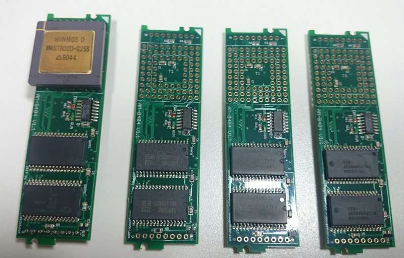
Good news! This time I created circuit diagram so you can actually make you own T2I2C – and that’s not enough: I’ve already laid out a TRAM-1 size circuit board using SMD parts of the C011 and 8574 making space for piggy-backing an Arduino Uno on top of that board.

But let’s start with the other details I mentioned the chapter before. I’m totally aware that there are many, many things to improve and optimize – and then there are probably even more I’m not aware of.
Here’s the how and why I did things they way I did:

Oneway

For this first version of T2I2C I’m using an C011 in ‘mode 1’ – that means it is offering actually two 8-bit buses, one for receiving (input, I0-7)) and one for transmitting (output, Q0-7). Because it’s quick and easy I don’t use the I-bus and therefor grounded it.
This means there’s no way for the Arduino to talk to the Transputer side of things. But using an extra bus for input would mean using a second 8574 and obviously using another 4 wires on the ATMega.

The elegant solution to this is using the C011 in ‘mode-2’ – it then behaves like a C012 which means it provides a single butbidirectional 8-bit bus. So why didn’t I used mode-2 in the first-place?
Well, while mode-1 just requires 2 lines for data-control, mode-2 needs 4 lines and some more coding in the ATMega ‘firmware’ e.g. handling the 2 registers provided by a C012 – So yes, I was just lazy and wanted results quick. The next release will certainly use mode-2.

Handshaking

So what is that data-control you’ve mentioned? Using 2 converters (C011/8574) in a row there’s obviously a need for all parties to know when data has arrived and needs to be processed.
The C011 as well as the 8574 provide a pin which flags a “hey, we have something here!” signal (QValid in the C011, /INT in the 8574) . But in contrast to the 8574 the C011 also needs an “Ok, got the data, feel free to fetch the next one” – which is called “QAck”. So the ATMega controls the data-flow talking to the C011 and completely ignores the 8574 which makes it somewhat transparent.
The comms protocol of the C011 can be found in its data-sheet here. It’s all about reading, holding and releasing QValid/QAck in the right timing.

First I was using an external interrupt line on the ATMega connected to QValid because it’s so obvious. But somehow the results were flaky – sometimes the ATMega seemed do choke on some bytes which simply didn’t make it through(*). After some cursing and hair-ripping I decided to switch back to polling – again because I was lazy and wanted to get results 😉
Up to now polling QValid just works great, probably because the ATMega is pretty fast and I2C is pretty slow.
(*) Yes, of course I’ve read all the docs about interrupt-programing and its caveats (short routines, volatile vars etc…) didn’t help.

Achtung! Kommando!

So what is actually going on in the ATMega running “Se Fiiiirmwarrre”? As mentioned in the previous chapter, I decided not to send a complete ‘bitmap’ of 128bytes each time an update occurs. Instead I created a simple command protocol, (currently) consisting of 3 bytes:

  • 1st byte: If < 255 it’s the number of the Transputer data. If 255 (0xFF) command flag set.
  • 2nd byte: If 1st-byte < 255, it’s the CPU-load in percent, else it’s acommand.
  • 3rd byte: If 1st-byte < 255, it’s the Memory-load in percent.

This means a single Transputer information update only takes 3 bytes. A command like “clear the display” is just a single byte.

Of course there are downsides. Updating a complete display of 128 Transputer-loads means sending 384 bytes instead of 128 bytes needed for a bitmap (512 pixels, 2 bits each = 1024bits = 128bytes) – But OTOH you could enhance the firmware for just that case: One command initiates a bitmap-transfer and then you send the 128bytes of data. Mind the could, i.e. this command doesn’t exist yet.

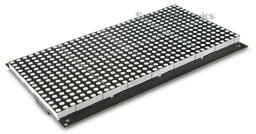
What comes on top of the handling/processing is the calculations needed to be done by the ATMega. There’s a command telling the ATMega how to setup the panel according to columns. If there are less than 33 Transputers to be displayed, each Transputers gets its own line of 16 LEDs. To display 64 Transputers, it will be divided into 2 columns with 8 LED each. 96 Transputers have to get along with 5 LEDs and 128 can only use 4.
No matter how many Transputers have to be displayed, poor ATMega first has to calculate the percentage value into 16, 8, 5 or 4 LEDs, then decide into which column this value goes and finally handle the displaying itself – worst case a 128 times. All this could be circumvent with a bitmap-transfer, offloading all those calculations to the sender (a Transputer in this case). But I’m not sure if this is much cleverer…

The Arduino source (.ino file) is available here. I suggest you have the Arduino Software installed.
There’s still debugging code in the source, putting out info on Arduinos USB/Serial port.

These are the commands currently implemented (in decimal):

001 – 015 : Set display brightness (0..15)
031 – 034 : Set the columns to be displayed (1..4)
099 : Clear the panel display
100 : Toggle CPU-load-only vs. CPU & RAM load mode

Hardware

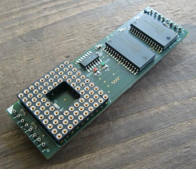
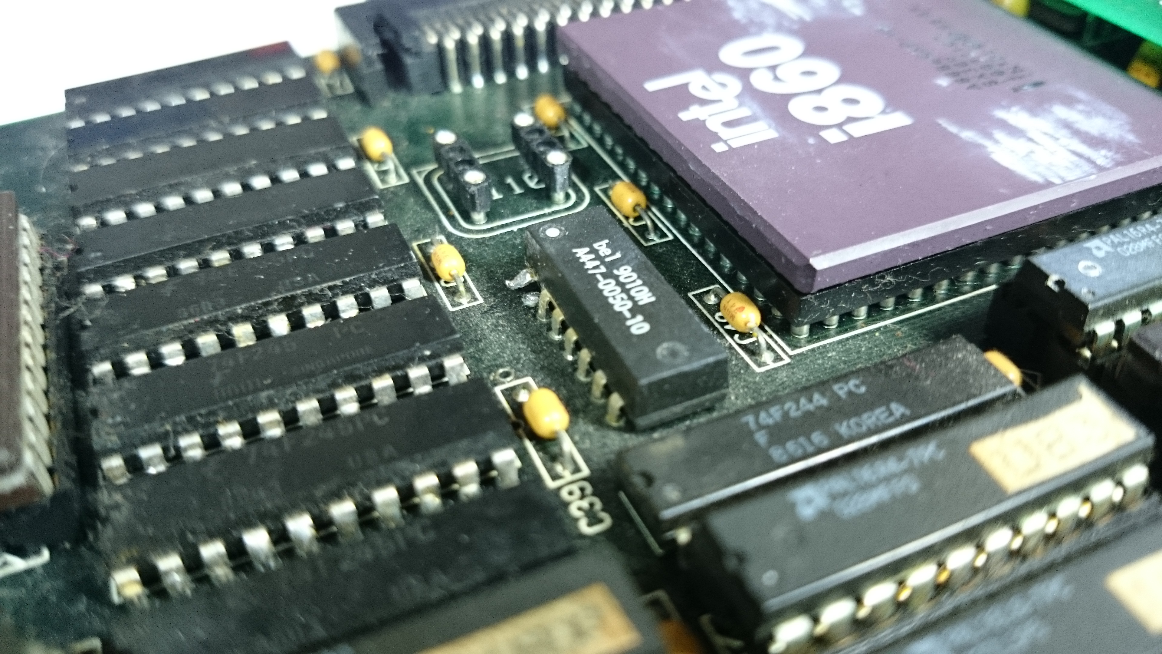
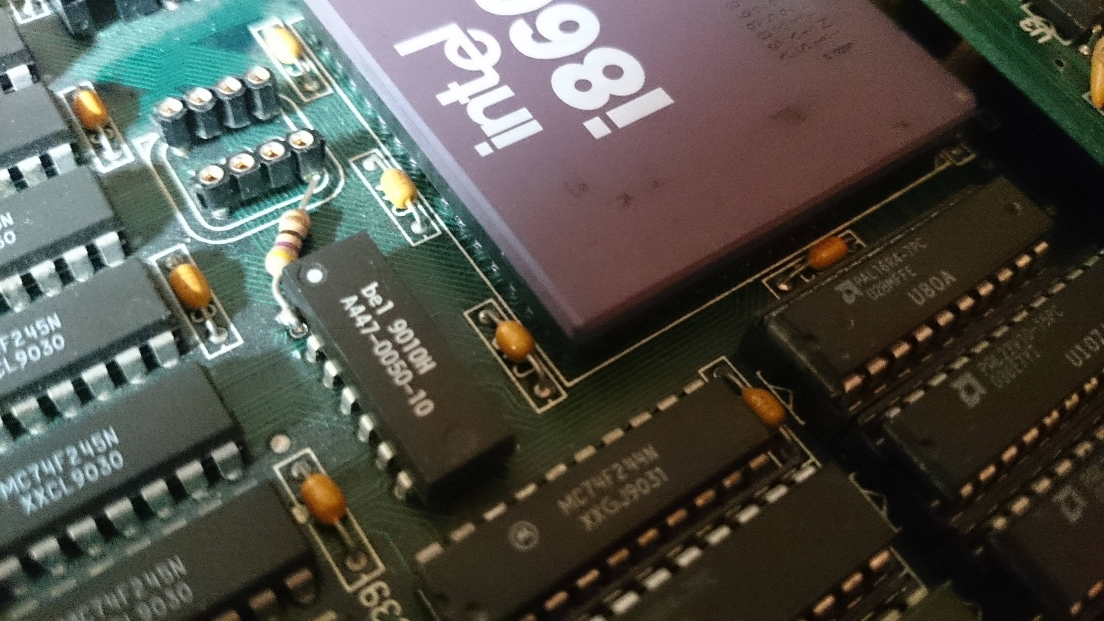
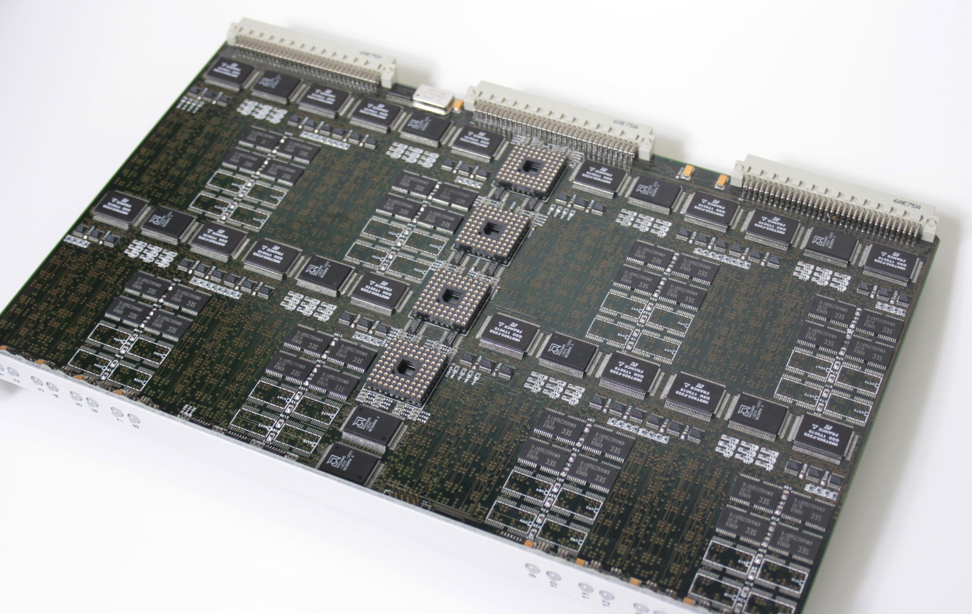
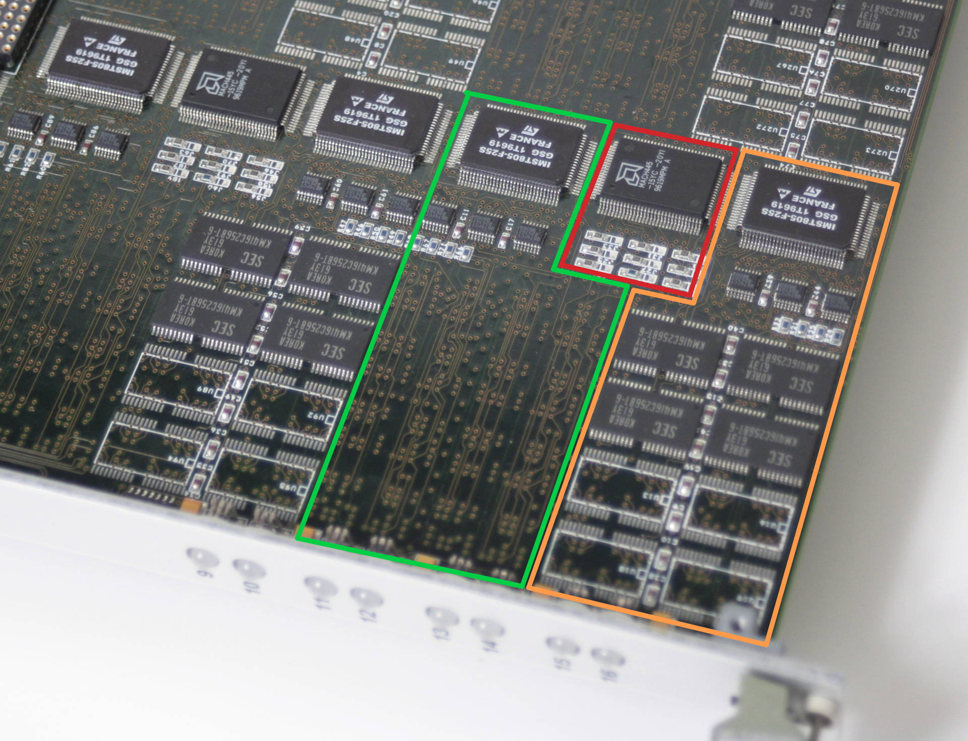
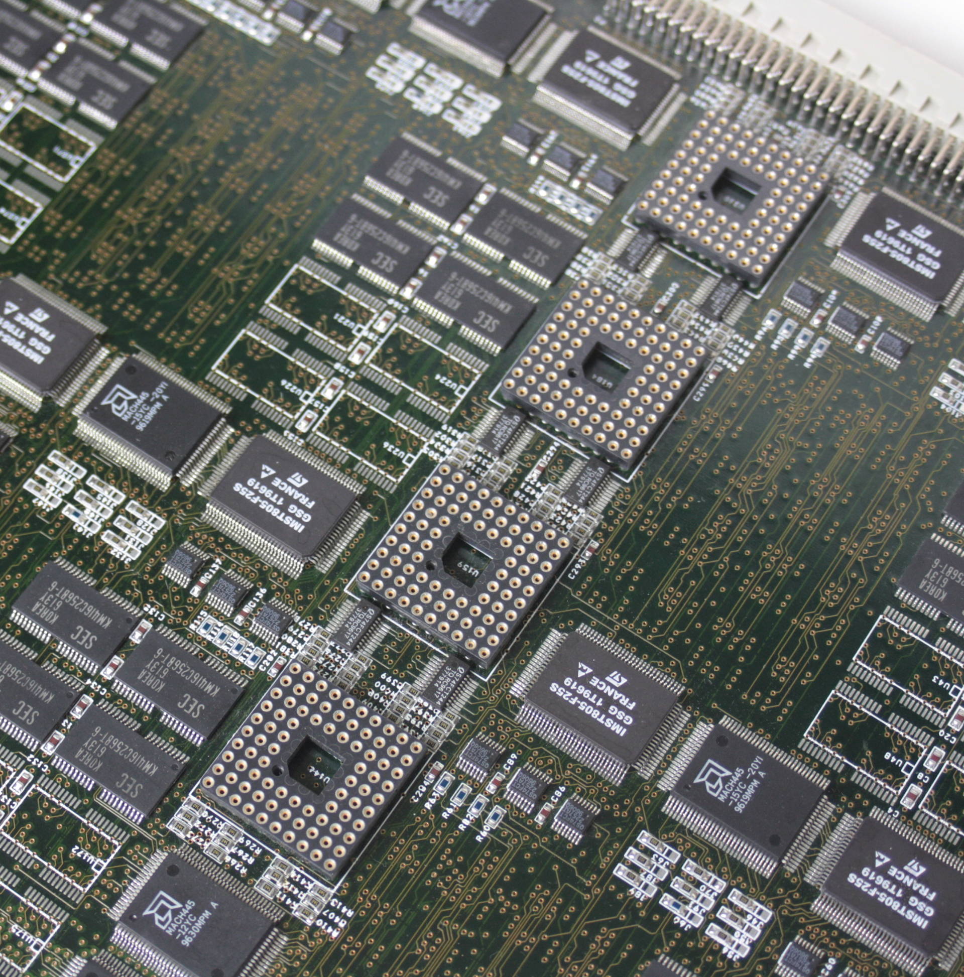
Like you’ve seen in the video, there’s no real circuit board existing yet there wasn’t a real circuit board around back then. But I’ve created a board layout for a TRAM-1 containing an SMD C011 and 8574 which provides the space needed for a socket to plug in anArduino Nano (the small version of an Arduino Duemilanove) – Version 3.x to be precise. You have to use a V3.0 or higher if you want to use my ‘firmware’ out of the box! This is because the analogue pins (A0-A7) have been rotated in V3.x and up – if you plan to use an earlier version of the Nano, you have to adjust the i2c-pin definition in the firmware source.
Anyhow – Using an Arduino Nano is much more flexible -and cost saving- than putting everything incl. the ATMega on the board itself.
The socket is laid out to be “double-row”, so you can still plug wires right next the Arduinos pins – well, actually this is mandatory at least for connecting to the LED panel.

Currently (v1.0) these pins are used/defined by the firmware on Arduino:

  • Portd: 7, 6, 5 and 4 for connecting the LED panel
  • Analogue input pins 4 & 5 (SDA/SCL) for the I2C bus
  • Portd: Pin 2 connects to QVAL, Pin 3 to QACK on the C011

board

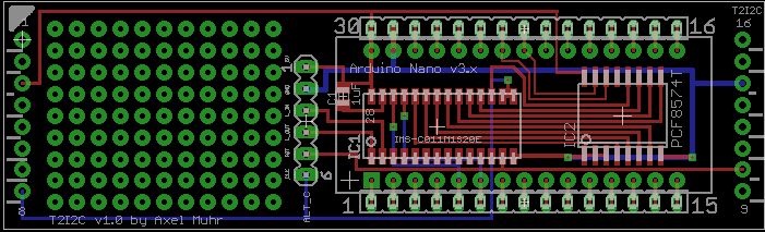
I tried to layout the board in such way that it could also be used as stand-alone, i.e. without being seated into a TRAM slot. Then you would have to provide the Links, 5V, GND, a 5MHz clock and Reset yourself via the alternative connector in the middle of the board, called “ALT_C” . There is still room left which I’ve used for a little breadboard section.

This design is to be considered v1.0 – still things to improve, especially a way to choose the link to be used if the board is actually plugged into a TRAM socket. v1.0 routes LinkIn/Out to the ALT_C socket which needs to be air-wired to the TRAM-pins… not nice but does its job.

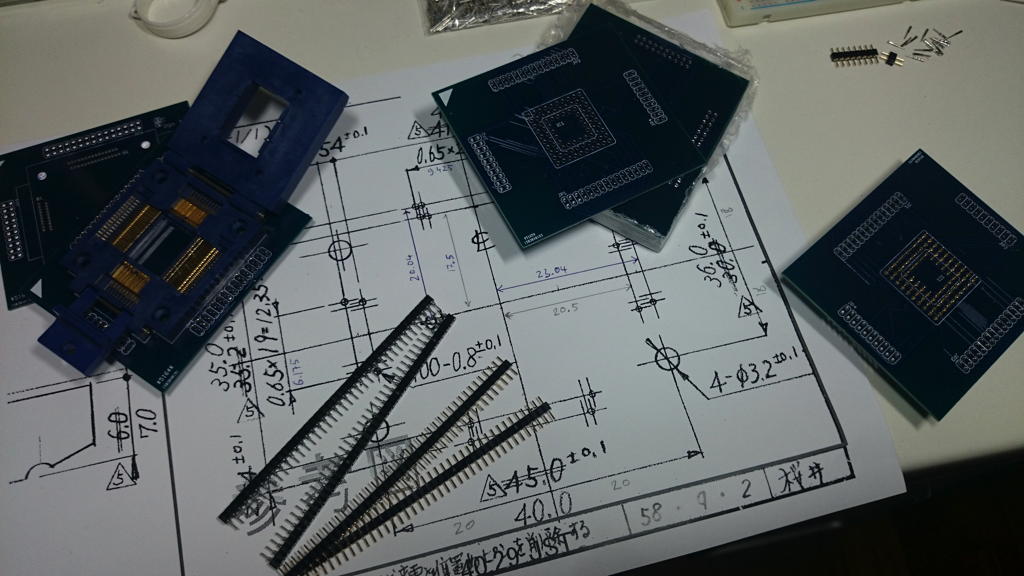
If interested, you can download the Eagle CAD files here.

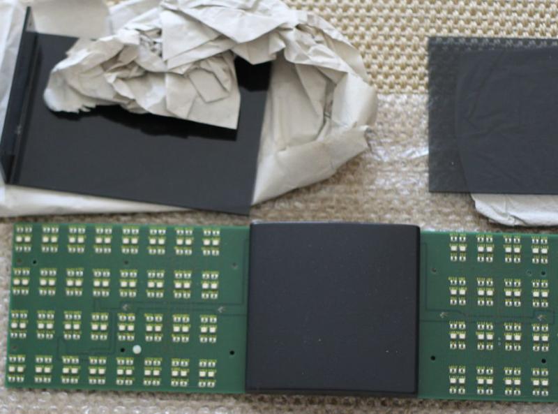
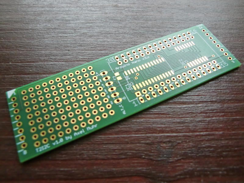
After nearly a year I was able to get a hand full of boards created and populated one using my brand new reflow oven (Reworked pizza oven) and voilá, here’s the T2i2c in flesh, naked:

T2i2c_naked

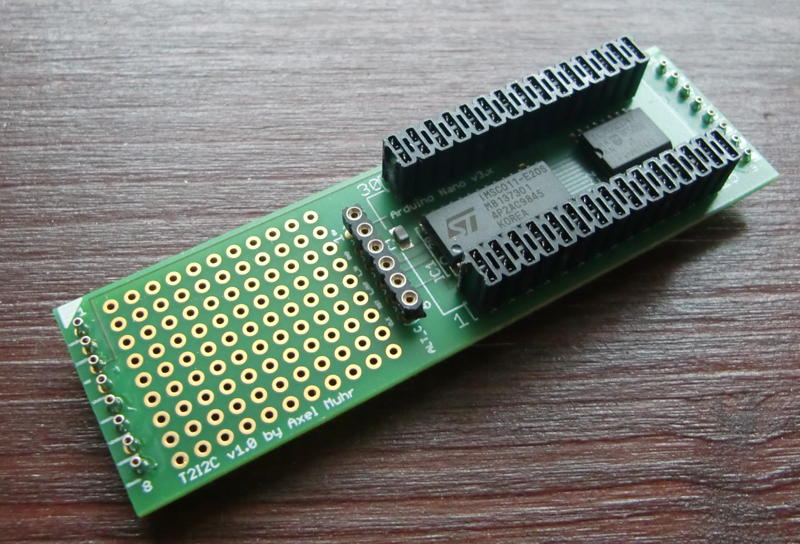
…a bit more dressed (all parts place)…

T2i2c_dressed

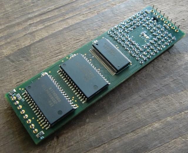
…and finally fully dressed (Nano plugged in):

T2i2c_fullyDressed

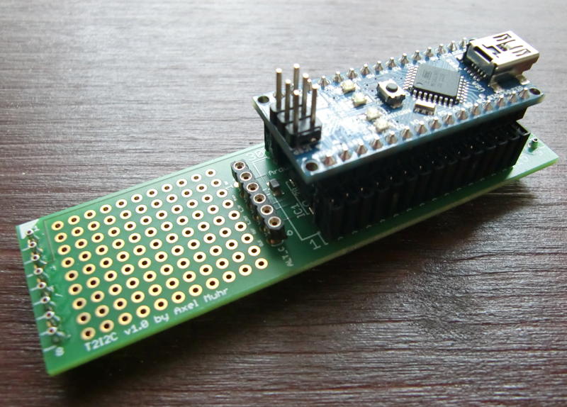
So the final question was: Will it actually work? Yes it did! I plugged it into slot 2 of my beloved BOZO, connected the LED panel and adjusted my Helios test-sources a bit, and tadaa:

T2i2c

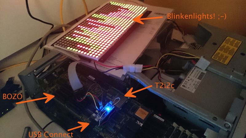
The cool side-effect of this project is, that you can keep the USB cable connected to your host, while the T2i2c is actually running in a system, giving a perfect  OS-link-sniffer for what’s going on in a Transputer setup.

Also, I reworked my Helios tools for checking the T2I2C functionality. Everthing is now in one single tool, i.e. test-pattern, clearing the panel or manually sending a command. Here’s the source as well as the executableread the source header before using! You can crash your Helios system – you’ve been warned!

Outlook

I won’t say the sky is the limit, but if the T2I2C-TRAM will be full-duplex in the next release (ie. C011 in Mode-2) driving an LED panel would be just one of many other uses this TRAM could fulfill.
Think of all the million things people did with their ATMega/Arduinos: LCD-Displays, SD-Card Interface, Ethernet and then some more. Ok, the speed of I2C will limit that somewhat (I already have made prerequisites in my ‘firmware’ to put I2C into 400kHz/kbps “fast mode”) but still a nice interface for connecting today-tech to your yester-tech.

The AM-B404

Here it is, my latest baby, the goal I was aiming for since years (4 to be exact) – not only to get more TRAMs for my systems but also to break the insane price spiral developing in the last years on ePay and other places. >300$ for a TRAM is crazy. Do not pay that amount! Even $100 is too much.

Update: Final version finished! Click here or scroll down for more.
Update 2: You can buy one, if you like…

AMB404-Front-small

My first CPU TRAM called AM-B404 in reminiscence to the IMS-B404 which comes closest to its specs:

  • Size-1 TRAM
  • 2MB low-power SRAM
  • 2 LEDs showing the Transputers status (running and error)

Well, the original Inmos B404 had 2MB DRAM, too (and additional 32k SRAM) but was a Size-2 TRAM and LEDs weren’t available on any Inmos TRAM… and we all know how important LEDs are! 😉 Contrary to the IMS-B404, the AM-B404 is low-profile, SRAM-only, so the whole RAM is accessed at 3-cycles vs. the IMS-B404 4-cycle DRAM.
Using a 6-layer PCB and all-modern SMD parts (well, as modern as 5V parts can get) the power consumption is a bit lower, too. I’d say about 100mA for the whole Board (no Transputer of course). Finally, there’s an easy access solder-bridge on the backside to set the CPU clock (20/25MHz).

AMB404-Back-small

This is just the 1st prototype. After thorough testing, I will optimize its layout a tiny bit and give it the proper shape of a TRAM. When that’s done, we’ll see how I can make you a realistic price offer.

UPDATE:

From Shenzen with love. The final PCB designes arrived and the first test went perfectly fine.

AM-B404stack

And here are the first 4 PCBs waiting to be finished with the Trough-Hole parts (i.e. Transputer Socket and TRAM Pins)… 100 solder-points in total… per TRAM. That’s quite a bit to solder :-/

First4

Video

Finally, here’s a short video showing the prototype AM-B404 in action (running Helios on my Inmos B020). The “exciting” thing is the blinking green LED which shows the CPUs activity. There’s even some brief red LED access (error) during boot-up which is triggered by Helios scanning the Transputer network.
The bright blue LED to the left is the T2i2c TRAM, so all TRAMs on the B020 are built by me now 😉

Want one?

If you hate the greedy ePay prices like I do, drop me a mail. I might have some AM-B404 left… even with T425/T800 Transputers.

Can I have the schematics?

No, not yet. Sorry. I have to break-even on this first…
Since people discovered there’s serious money in the retro-scene, some ‘smart guys’ started to clone every PCB they can get their hands on and thereby steal the initial investment which the original creators made.

I sell them a bit over the price they cost me to produce. And trust me, you won’t be able to go lower than me:
It’s a 6 layer PCB. ENIG Gold.
Sadly SRAM did not get cheaper, really. Especially the (obsolete) 5V 512kx8 I’m using were lately discovered by other projects to be very convenient and so the battle for SRAM was on. If you’re lucky you might get one for 4€… and you need 4 of them.
The 16 pins used to connect the TRAM to its carrier are very special. You have to buy them by the 1000s – 0.15€ a pop… you do the math.

QFP Adapter

Again, a man had to do, what a man has to do…
My good friend Udo gave me some Transputers in QFP package, most of them previously used and unsoldered from some PCB. Nobody knows, if they are still OK or already braindead – so I needed a QFP Adapter.

As fate goes, some fine day I stumbled across a nice 100pin QFP burn-in socket from Yamaichi on ePay. Yamaichi is “the other company” producing burn-in sockets besides 3M with their Textool brand range.
Normally those sockets are insanely expensive (100US$++) but this was a lucky buy – well for the “price” that it was an EOL model… for many years. This means no documentation available. But the very kind sales team of Yamaichi Germany (Vielen Dank Frau Howe!) was able to dig out a hand drawn blueprint of this very socket, model #IC51-1004-139.
This valuable Information at hand I was able to create my own Eagle CAD device for this Socket – not an easy task as most measures were not directly given but had to be calculated using other documented distances. After some hours I ended up with two PCBs, one for the burn-in socket which again will be mounted onto a PGA-Pin adapter PCB.
When done it was time for another “first”: Try the DirtCheapPCBs service. 2 Layers, 10x10cm PCB, 10 pieces for just US$25 (incl. shipping) – almost cheaper than doing it yourself.
After two and a half weeks I had two stacks of 10 PCBs each. Anxiously I tried if the socket with its tiiiiiiny pins will fit…. and… it… did! Hooray!! I didn’t expected that but everything fit perfectly, even the silkscreen. Soldering the 0.025″ pitch was another story…

But see for your self. Upper left corner you see the burn-in socket already soldered. At the right edge, the lower PCB it waiting to get 84 Pins soldered for the PGA socket… and another 100 to connect to the upper PCB.

QFPAdaptor

Feel free to contact me, if it happen to be that you also found an IC51-1004-139 socket and need the Eagle lib or even the PCB for it… I have 9 of them left 😉

Upgrading the NumberSmasher

After a long time, I had a look at my 3 NumberSmashers again. Looking closer, I spotted a difference.
One had a silkscreen print saying “V1.2” while the others were “V1.1”. So why not upgrading the NumberSmasher yourself?!

Step 1

The most obvious fix the V1.2 had was a 47ohm resistor fitted between one pin of the 40MHz oscillator and pin-1 of an IC called “A447-0050-10 “. That’s a “10 tap leading edge delay module” made by Bel Fuse Inc.. Pin 1 takes the input signal and each other pin  adds a delay of 5ns.
So I assume this fix was meant to reduce noise on the delay chip input to make its output cleaner.

Anyhoo, here’s the quick and easy howto. The below picture shows the section of a NumberCruncher V1.1. near the almighty i860. Next to it is the (now empty) socket for the 40MHz oscillator. Next to that you see the 10-pin delay chip which pin-1 already had been cut and slightly bent upwards.
We need a bit of pin-1s leg so when cutting it, be sure to cut it as close to the board as possible!

NS_premod.jpeg

Now for the next step. Get a 47ohm resistor and shorten its wires to bridge the space between the bent leg of the delay chip and the output pin of the oscillator (see below picture).

NS_860_postmod.jpeg

To make things perfectly clean, remove the pin remains by flipping the NS860 over and pull the remains with your solder iron and tweezers.

Step 2

I thought this would be a simple fix, too. There are some retrofitted jumper-wires on the back of the NumberSmasher near the ISA connectors.

NS860_patchwiresI’ve color adjusted the photo to make the wires more visible. Colored arrows show start and end of each wire

But taking a look at the chips those jumper-wires are connected, it showed that the two PAL22V10  of the V1.1 board were replaced by two PALCE610H – which is a completely different beast, same number of pins, everything else varies:

max in max out macrocells Specials
PAL22V10 22 20 10
PALCE610H 20 16 16  D, T, J-K or S-R Flip_Flops, counters and large state machines possible

Additionally here’s a side-by-side of the pinouts. This immediately explains the two long jump-wires from pin-1 to pin-13 (red & blue arrows) which connect the two clock inputs.

20v10_610h

Here’s the PALCE610 in place:

PALCE610It’s the one at the bottom in the middle (named U93) and one hidden beneath the link-interface board (U-88).

My assumption is, that the PALCE610 has a completely different programming and the jump-wires just support the changes made, i.e routing the outputs of pin3 to input pin2 (green) respectively pin4 to pin 2 (pink) .

Next up: I will get out my Über-Programmer and try reading it – but I have low hopes, as MicroWay normally set the protection fuse on all the GALs/PALs they used.

Update

Wow, that was unexpected. Both PALCE610 hadn’t had the protection fuse set – at least on my retro-fitted V1.1 board. So lo-and-behold, here are the JEDEC files for you to program your own PALCEs!  And because I couldn’t resist, I’ve disassembled the JEDs and added the PALASM code in the archive, too 😀

That said… it’s completely unclear what had been changed from V1.1 to V1.2 (well, U93 being close to the ISA connector gives a hint) and under which circumstances an upgrade is necessary at all.
But if you own a 1.1 and it behaves strange, you should give it a try.

Nostalgia

After the NumberSmasher, MicroWay presented the “QuadPuter”, an EISA-Bus based quad-i860 monster… which had a short lifespan and was, well, expensive as expected. 31000 German Marks was exactly what you would have payed for an Volkswagen Golf mkII GTI 16V back then… one of the hottest hot-hatches you could get.

I found this snippet in one of my (German) computer magazines (“MC”, 1993) – they mention the OS860 (for DOS) as well as the MAX860 multiuser-OS for UNIX, OS/2 and DOS:

Transtech TMB316

The Transtech TMB316 never really seemed to see the light of day and is probably one of the last Transputer developments of AG Electronics for Transtech. Internally it’s also been called the “MTPA-0001”, MTP translates into Multi Transputer Platform, most likely “A” for 2MB and version 0001.

It’s a triple-height Eurocard board featuring 16 T805 at 25 or 30MHz, each with 2 or 4MB RAM. This is the card in full beauty:

TMB316_total

As you can see, it’s not totally cramped with parts and actually has quite uncongested areas. The reason for that is, that this model (Called TMB316-2-25) only uses 2MB of the possible 4MB RAM per Transputer and while all Transputers are placed on the top side of the PCB, every second Transputer has its RAM on the bottom side, right beneath the ‘free space’ visible on the top. This is the back side (flipped horizontally):

TMB316_back

It becomes more obvious, when we zoom into a Transputer section of the board:

TMB316_nodes

I coloured each Transputer (green and orange) with its RAM area. The red area shows the CPLD which is shared between the two Trasnputers and handles the DRAM control and such.
Also visible on the cards front panel are 8 of totally 16 LEDs which display each Transputers status.

Obviously meant for a bigger systems, Transtech/AG Electronics planned the TMB316 for big deployments, i.e. more than one card. So each card uses four C004 link switches which connect the 16 T805 to each-other as well as to the outside world via the DIN connectors at the back of the card (totally non-standard pinout). This is fine if reconfiguration of the T-network is important but there’s no alternative but using dummy PCBs if all you need is speed. And being an avid GeekDot reader, you know my view on C004’s 😉

TMB316_C004This is where the C004s were meant to live.

Just in case you really want to know, here’s how the Transputer nodes are connected to the 4 C004 and to the backplane connectors:

TMB316_C004_links

Inmos B004

I’d call the Inmos B004 the “mother of all Interface cards”, simply because it was the first ISA card sold by INMOS. And it wasn’t just the card but it also defined the (PC) standard of the software interface, mostly called the “B004-interface”. What a surprise 😉

So being the first card, it is quite big (full ISA length) while not offering really impressing specs: 8bit XT Bus, just one Transputer –TRAMs weren’t invented yet- and a max. of 2MB RAM (DILs). To do it justice, the manual rightfully calls it “Evaluation Board” and for that purpose it’s totally fine – remember that 2MB were quite an amount of RAM back in 1984.
To create a multi-Transputer network you had to either plug-in multiple B004s or connect an external network to the onboard connectors (the blue ones in the picture below).

As mentioned, the B004 software interface is what makes this card a keystone in the Transputer universe. All communication to the host (i.e. the XT/AT compatible PC) is done through a port range normally beginning at 0x150 (base, can be moved by some cards).
With certain offsets the host software can communicate with the Transputer, or the C011 to be precise:

Base Address Register Comment
+0x00 C011/12 input data  read
+0x01 C011/12 Output data write
+0x02 C011/12 input status register read = returns input status
write = set input interrupt on/off
+0x03 C011/12 Output status register read = returns output status
write = set output interrupt on/off
+0x10 Reset/Error register write: Reset Transputer & C011/12 and possibly subsystem (check manual)
read: Get Error status
+0x11 Analyse register  (un)set analyse

This mapping was used by more or less all ISA interface cards and extended by other more sophisticated interface cards later.

Clones

Needless to say, that very soon there were a couple of “inspired” models from other manufacturers. AFAIK all of them support Transputers up to 30MHz, which the B004 didn’t… so they’re actually better.

This example is from Microway (yes, those guys who later build the i860 Number Smasher), named Monoputer and dated 1987. Up to 2MB could be used on it. Mind the connectors being accessible from the outside:

Microway-B004

Later they produced the “Monoputer 2” which was more modern and used SIMM RAM modules instead of DIL parts. The Transputer and Linkinterface moved into the middle of the card and the link connectors were moved inside the pc case again – the connectors are the very same used on the NumberSmasher860:

monoputer2

And here’s the one Transtech made, calling it TMB04 mind the SIMM banks which enable the card to give home up to 16MB RAM (at 3 cycle speed!):

Transtech TMB04