
It was about time for a new section to be added: ” Systems”
This is the place where all the different cards from the Hardware section will be fired up to flex their muscles. First somewhat finished system is Kerberos, a three i860 CPU system.
All posts by Axel
Kerberos
Kerberos is the machine I’ve specifically built for hosting all 3 DSM860 cards I own.
The name was chosen because the hell-hound Kerberos (Latin ‘Cerberus’, Greek ‘Κέρβερος’) is mostly depicted with three heads and the Greek myths offer innumerable possibilities for a nice g[r]eek name space 😉
The quest for the right motherboard was not easy. It should be small, still featuring as many EISA slots as possible. In the end it became a Gigabyte GA-486SA having some quite unique features for its time:
- 8 EISA slots
- 2 of them also having Vesa-Local-Bus connectors
- A Weitek 4167 Socket
- 8 SIMM slots
Because it was clear I will use-up 6 slots just for the 3 DSM860 cards (being sandwiched boards) I wanted to fill the remaining 2 slots as clever as possible.
After another year (!) of searching I was able to get my greedy little hands onto a Western Digital ‘Ports’o’Call‘ Vesa-Local card. This is a rare do-it-all card saving lots of slots, specifically:
- WD90c33 VGA (1-2MB) connected to the VL-Bus (fast!)
- Appian Local Bus IDE controller (also quite fast)
- Floppy controller
- 2S/1P peripheral controller
In a sentence: Everything a basic system needs to work! The remaining slot was planned for a NIC making the system complete.
Because I was expecting quite some heat coming from the three i860 I’ve opted for a desktop case so that the heat can easily dissipate through the open casing – also I was prepared for lots of plugging and unplugging of cards, jumpers etc. which is much easier with a desktop case.
Golden Rule #1 of hardware fiddling: One step after the other!
So before filling the system up to its rim, I started with just one DSM860. It quickly became clear that there was no way in using the ports’o’call’s WD90c31 as the server running on the DSMs does only support certain VGA cards (if you like to have graphic output), namely some very obsolete, non-standard Genoa cards…and in its latest version: Good old ET4000!
So the nice ports’o’call had to make place for a standard multi-IO controller and the 2nd slot was used for an ET4000. That setup worked quite nicely!
After the last DSM860/32 board was fixed, I was ready to “stuff that turkey”.
One card after the other went into the slots – that’s what I call a crowded house:
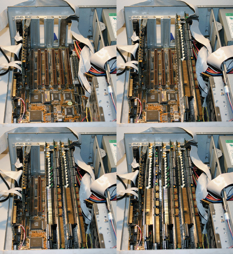
As the animation above is not the highest quality (file size!), here are some more shots…
All seats taken, sorry:
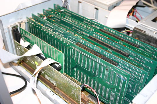
The money-shot 😉 Indeed… in 1991 you would have payed 48.000 German Marks (~US$ 24k) for the DSM860’s alone… plus a 486DX/2 system with a whopping 32MB of RAM (~9500 Marks = ~US$ 4750). So that’s a total of $US 28.750 or the average income/year (1991) in the US.
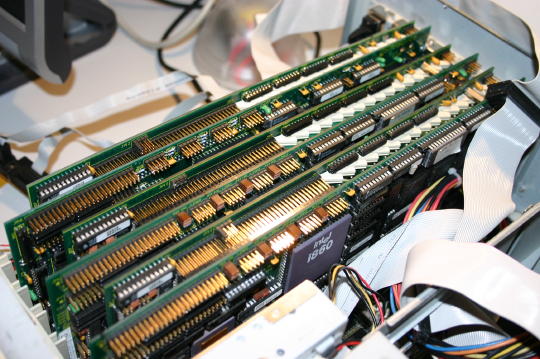
Finally some of Kerberos facts:
- 3 x i860/40MHz each 8MB RAM (= 180-240 ‘marketing-MFLOPS’ / 360 ‘marketing-MIPS’)
- Handcoded code using LINDA SMP techniques can realistically reach ~80 MFLOPS on this system, that’s about the speed of a Cray-1 or … a Pentium Pro 200 :-/
- 1 x 486/DX2-66, 32 MB RAM (~3.5 MFLOPS)
- Complete system (w/o display) draws 140W when running full steam ahead. Which is about the same a recent (’09) Intel Core2/Core i7 or AMD Phenom needs @ 3.2GHz – just the CPU though!
Fixing scratched traces
This is the price you have to pay if you’re into real men’s hardware:
Being (falsely) identified as “old crap”, some cool things end up in the dumpsters… or worse. Being tossed around in some storage for years, probably stacked with other cards and boards, it might happen that some traces on the outer layers got badly scratched, thus making the board/card non-working. Here’s how I try to fix scartched traces… and most of the times it works:
First make sure that the circuit path (trace) is really broken – I just may look like, but isn’t.
To do this you need a volt-meter. Follow the suspected trace in both directions until you find a pin or through-hole it is connected to. Use these two points to test if the trace is still connected.
Ok, damn, it’s broken 🙁 You need three things:
- A sharp knife or scalpel
- Adhesive tape (Scotch, Tesa or whatever it’s called in your corner of the world)
- Conductive (silver) lacquer
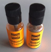
Conductive-what? Conductive lacquer is actually a cool thing to play with… but be prepared: It’s not cheap (about 9-10 Euros). It comes in tiny bottles or as a pen, which is even more expensive (20+ Euros). The bottles look like this (lacquer and diluter):
Ok, the process is quite simple:
- Use the knife to scratch-off some of the coating lacquer on both ends where the trace was “cut” until you see some copper shining through.
- Check with your volt-meter that you actually have contact with one end and e.g. a pin on the other end of the trace. Do this for both “halves” of the cut trace.
- Mask the place you’re going to ‘heal’ with your adhesive tape – this prevents the conductive lacquer to run all over your board.
- Apply the conductive silver lacquer onto the spot you’ve just masked and let it dry (read the manual that came with the lacquer – yeah it’s unmanly but nobody will see you ;-))
- Using your volt-meter, check again. This time from both ends of the complete trace.
If you’ve done everything right, the trace should work again – and so does your card/board! Yay!
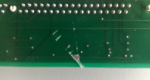
Here’s how my badly scatched MiroHIGHRISC looks like in certain places – can you spot the little silver dot?
Final hit: Some lacquers are quite thin on silver (blame the manufacturer) so after some days the spot you just fixed might become unreliable. In this case you might repeat the procedure to get more silver to that spot.
Removing pin rows
Removing pin rows…doh! It took me quite some time to figure out a working solution for this problem, so I thought it might be useful to you some day, too.
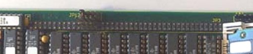
Some idio^h^h^h^h not so clever person cut off all the pins on one of my DSM860 RAM boards – I probably will never figure out why (may a lightning hit him!). Besides 8 of the pins all other 74 (!) where cut, rendering the ram card non-functional (it’s the memory bus connector).
Here’s a (blurry enlarged) picture of the mess:
I started to desolder some pins from the back-side of the card but soon found out that the solder was too old to be removed the classic way (desolder pump & wick). Also, that pin-row (41×2) was one piece, so I would have to completely remove all the solder before I would be able to pull the part from the card.
After some thinking I came to this solution, which worked quite good:
First you need to cut away the plastic part from the top of the board. I used a very fine and sharp caliper to cut away one pin after the other (i.e. like a single jumper).
While doing so be careful not to cut into the board!
Then pull or push the plastic pieces from the pins, again one after the other – I used a thin knife pushed under the plastic an gently wiggling it over the pin.
When done, it should look like this:
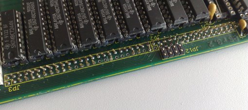
You may spot that some pins are missing already – that’s because my previous desolder tries sometimes seemed to work. Still, I couldn’t avoid that some pins got bent. This is the time for my secret repair tools: Syringe needles!
Second, get two kind of needles: Gauge 18 and 20, that is 0.9mm and 1.2mm, color code yellow and pink. Cut off the tip of the needles and use a rasp to make the edge straight and clean. They should look like this then:
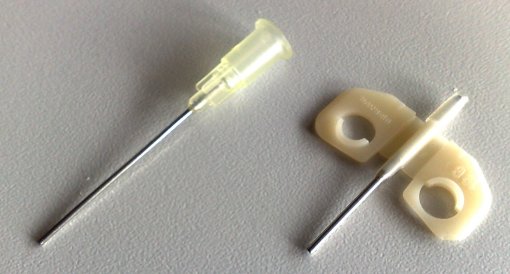
The bigger needle (G20) is just perfect to be completely pushed over a pin which then can be bent into any position without the risk of breaking it off – it works like this:
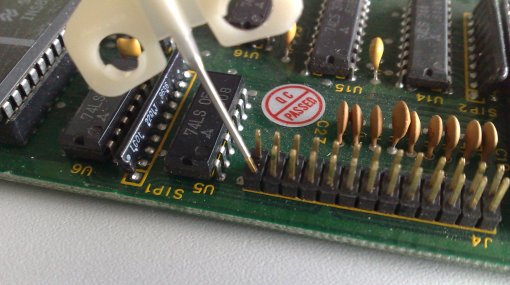
(This is just a showcase picture with a different board, the needle needs to be pushed all the way down over the pin)
So straighten all the pins into an upright position. This will be important for the next step!
Now put your board into a vertical position (e.g. fixed by a bench vise or clamped between your inner thighs ;-)), get out your solder iron and the G18 needle – this needle should be just small enough to fit through a pin-hole.
This is the third and last step. Place the G18 needle over the pin you like to desolder on the back-side of the board like showed here:
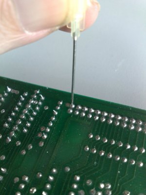
From the other side you’re touching the base of the pin with your solder iron. As soon as the solder starts to melt gently push the needle onto the pin.
If everything works like it did for me, you will push the needle through the board, including the solder and the pin you’ve planned to remove!
The great thing with this is that the needle (being made of steel) does not stick to the solder. As soon as the needle got a bit colder, you can easily remove the pin as well as the excess solder from the needle with your fingers!
Now carefully pull back the needle through the board and you should have a nice and clean through-hole in the board. If not, a final cleaning with a desolder-pump or wick should do it.
This needle-trick also works brilliantly with empty pin-holes which got filled with solder. Just place the needle on the pin-hole on one side of the board, heat up the solder on the other side while pushing the needle. Pop! There goes the solder!
As said, this technique worked great for me. All 82 pins got removed, a new pin-row was soldered into place and the card is now working like a charm.
Still, do this at your own risk!
I’m not going to be taken liable for any damage to your board or your health!
If your unsure if you are able to perform this stunt, don’t do it!
Practice with an old scrap board/card before you fiddle with the “real thing”!
New DIY acticles
It’s been a bit quiet lately – that’s due to me fixing some of my prrrrrechious things.
If you have some cards with scatched traces or broken parts you cannot desolder, you might want to check out the DIY section.
The Godzilla of all 486 boards!
Finally I managed to beef up the Hauppauge 4860 section. Come join me drooling over one of the most exciting 80486 mainboard ever made!
Welcome MIPS
Not only did I add a new CPU-family into the hardware category but I’ve also added quite a rare accelerator card: The miroHIGHRISC, an ISA card featureing a MIPS R3000 CPU. This is the only place in the web to read about it!
miroHIGHRISC & miroTIGER
This is indeed a very rare breed – I was informed that less than a 100 of those were sold. Built in the end of 1992 as “Project Zorro” by the German company miro (bought by Pinnacle in ’97) it took the same line as all the other accelerated graphic cards in those days: Highspeed graphic -mostly TIGA- plus some speedy general purpose CPU. The SPEA cards using Intels i860 were direct competitors for example – I was also told that miro also looked into using the i860 but scrapped that attempt in an early stage in favor for the HIGHRISC.
The Miro HighRisc -or miroHIGHRISC as they wrote it back then- was a full-length 16-bit ISA card containing a MIPS CPU and a maximum of 32MB of RAM.
Technical facts:
- 33MHz LSI LR33050 CPU which is a R3000 clone including the R3010 FPU minus MMU
- 1k data- and 4k instruction caches on-die
- 33 MIPS / 33 MFLOPS
- 8-32 MB RAM plugged into up to 4 SIMM slots
- 32 bit bus to connect the miroTIGER graphics card (100MB/s)
- 2D: 150000 Vectors/s of 10 pixels length
- 3D: 10000 triangles/s of 100 pixels, flat-shaded
- 6000 triangles/s of 100 pixels, Gouraud-shaded
miro claimed that the HighRisc would deliver nearly twice the performance of an i860/33 solution with “real-world” applications (namely AutoCAD 12). That has yet to be proven but sounds reasonable given the limitations the i860 had when used as general purpose CPU.
Here’s the HighRisc in its full glory:
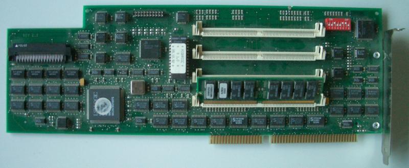
Interestingly, there’s next to none information on the Web about this card. Probably due to its high cost (5700DM) and the failing TIGA standard.
Here’s a nice snippet from an interview (in German) from 1999 with the original product manager Frank Pölzl:
Q4. What was your biggest flop?
miroHIGHRISC, a 3D-graphic card with MIPS and TI-Graphic-Processor.
Another tasty detail is that according to a news-snippet from the German magazine c’t (12/99, p.22) this card was developed in cooperation with Silicon Graphics (SGI) which bought MIPS some years before. Maybe this was SGIs first and last attempt to get a foot into the PC market?
Yet another interesting fact: The LSI 33k CPU was later radiation hardened by a company called Synova Inc., rechristened as “Mongoose V” and as such traveled into space several times… even to Pluto!
Here’s the left side of the card in more detail. It contains the CPU and the BIOS (32k EPROM dump available here) lots of 74-logic ICs, GALs and some MACH PLDs.
At the top-left corner of the picture below you see the connector to the miroTIGER, a TIGA graphics card described a bit further down on this page.
Also, there’s an undocumented 20-pin connector at the upper-right edge of the card. This might be the 16MB/s interface “to connect peripherals like laser printers or repro-devices” as mentioned in the c’t article. Thinking about it – it’s an interface to an UART. This will be a nice project to do further investigation.
The pinout (the connector is rotated 90° clock-wise):
GND oo /WR0
D0 oo INT2
D1 oo /RD
D2 oo /IOSEL
D3 oo (unknown)
D4 oo A2
D5 oo A3
D6 oo A4
D7 oo A5
VCC oo A23
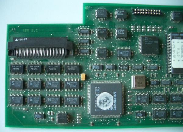
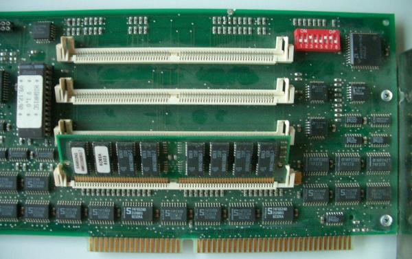
The right side of the card is dominated by the 4 SIMM slots which, according to the manual, support up to 8MB each. Also there’s a DIP-switch for setting up the address-range etc.
Even it has nothing to do with MIPS, the accompanying graphics card miroTIGER fits in quite good here. This card was meant to run for itself or accelerated by the above described miroHIGHRISC. This is what it looks like:
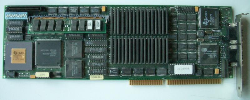
Following the TIGA standard it naturally features a TMS34020 graphics processor. This processor has its own RAM to do all the calculations, display-lists and fonts. Because TIGA was completely incompatible to the usual CGA/EGA/VGA standards you had to have such a card installed in parallel to see all the DOS/Windows outputs before switching into TIGA-mode. The normal setup was to have a 2nd high-res (1024×768++) monitor connected to the TIGA card then.
More advanced cards like the miroTIGER also had a VGA chip on-board, which saved you a slot and all the extra hassle. So let’s have a look at the details:
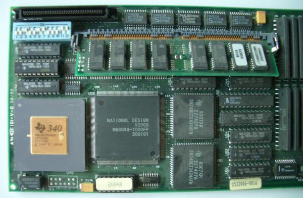
This is the left side of the card. The nice golden chip is of course the TIGA processor. Next to it there’s a National Design V2000 chip – most probably an ASIC doing all the RAM handling and stuff.. accidentally I stumbled across a notion of a “National Design Volante2000” TIGA card. Smell the relation here? So my most recent assumption about this is, that’s a somewhat standard TMS340 glue-chip, licenced by National Design to other TIGA card manufacturers.
The SIMM above is 8MB of RAM for the TMS340. Depending on the PAL (labeled 2004, 2044 or 2084) on the lower edge of the card, one could use 0, 4 or 8MB of RAM.
On the upper left corner is the connector to the miroHIGHRISC card as well as an impressive row of DIP switches.
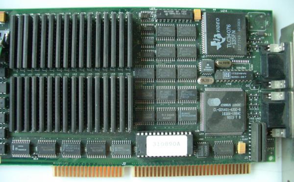
The right side is mainly occupied by 4MB VRAM for the TMS340 as well as the TI RAMDAC in the upper right corner.
Below is a very simple onboard VGA controller by Cirrus Logic (CL-GD5401 aka Acumos AVGA1) and next to it its puny 256k DRAM – which is the maximum a GD5401 can address by the way :-/
This is a good place to post a big thank you to Peter Huyoff – the wonderful guy who saved my life while doing the ‘research’ on this card.
As you might spot in the picture above, there’s one chip broken… a tiny 74AS74 flip-flop – try to find a single SMD AS74 these days. It’s impossible if you’re not prepared to pay $50 b/c of minimum order fees! And no, an F74 doesn’t do it, it’s still too slow. Been there, done that.
Peter provided me another working miroTIGER for free! That’s the spririt between real men! And Peter is definitely one of them!
Kontron SBC860
First of all: I do not own this card, I just list it for completeness.
Everything written here is accumulated through computer magazine articles or internet sources – if you know more or better, I’m always happy to hear from you.
This is a picture of the Kontron SBC860 (courtesy of Jörg Heilmann):
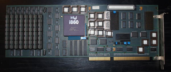
As you can see the SBC860 is much higher integrated as all other i860 cards presented on this page (while it bears quite some similarities with the rev.1.6 of the DSM860-OEM/16), most parts being used in modern SMD form.
It’s a single, full-length 16-bit ISA card, featuring 8 proprietary SIMM slots for up to 32MB RAM.
As far as I can see, the SBC860 has its own bus-interface so no fancy Transputer-Links or such.
In the upper right corner of the card are two huge “pin arrays” (each with 112 pins), the left one having two blue jumpers set. Iassume this could be some sort of expansion-bus for add-ons. Interesting fact: Exactly this part was missing on the board which was reviewed in the German magazine c’t 91/3. As Jörgs card says “R14/A” on one label this might hint towards his card being a later, updated version.
The price of the card was as hefty as their competitors: 33 MHz/8 MByte 13212 DM, 40 MHz/32 MByte at ~21200 DM in the year 1991 (US$ was roughly half)
P3 = Interrupt Vector
7 10 11 12
: : : :
P4 = I/O Base Address 8 consecutive Port Adresses, between 0x100 and 0x3F8
P4 I/O Addr
==============================
::IIIII 0x300
::II:II ::: 0x320
::IIII: ::: 0x308
:I::III 0x200
Some NumberSmasher progress
Thanks to another i860 fanatic enthusiast I have some more details on the Microway NumberSmasher!
Umh, yeah – and happy new year y’all!