All posts by Axel

http://www.geekdot.com/about-me/

Transputer Software

This is my little pool of Transputer software… while my main interest lies in the area of getting them run (and lots of ’em ;-)), you come to a certain point you actually want them to do something.

Don’t expect megabytes of software here… go over to Rams software section, he collected/rescued nearly everything which was available on the market.

Transputer network visualizer

I’m an “eye-person”, and looking at bigger ipsy or rspy network map files does not reveal the Transputer network topology at the first glance.
So I wrote a little tool, the “Transputer network visualizer” (TNV for short). It reads an ispy/rspy output file (extension “.OUT” was a random invention of mine) and tries to make visual sense out of it. So it starts with a Tree view.
Use the click & hold the right mouse-button to pan the view. Mouse-Wheel (or “+/-” keys) will zoom.
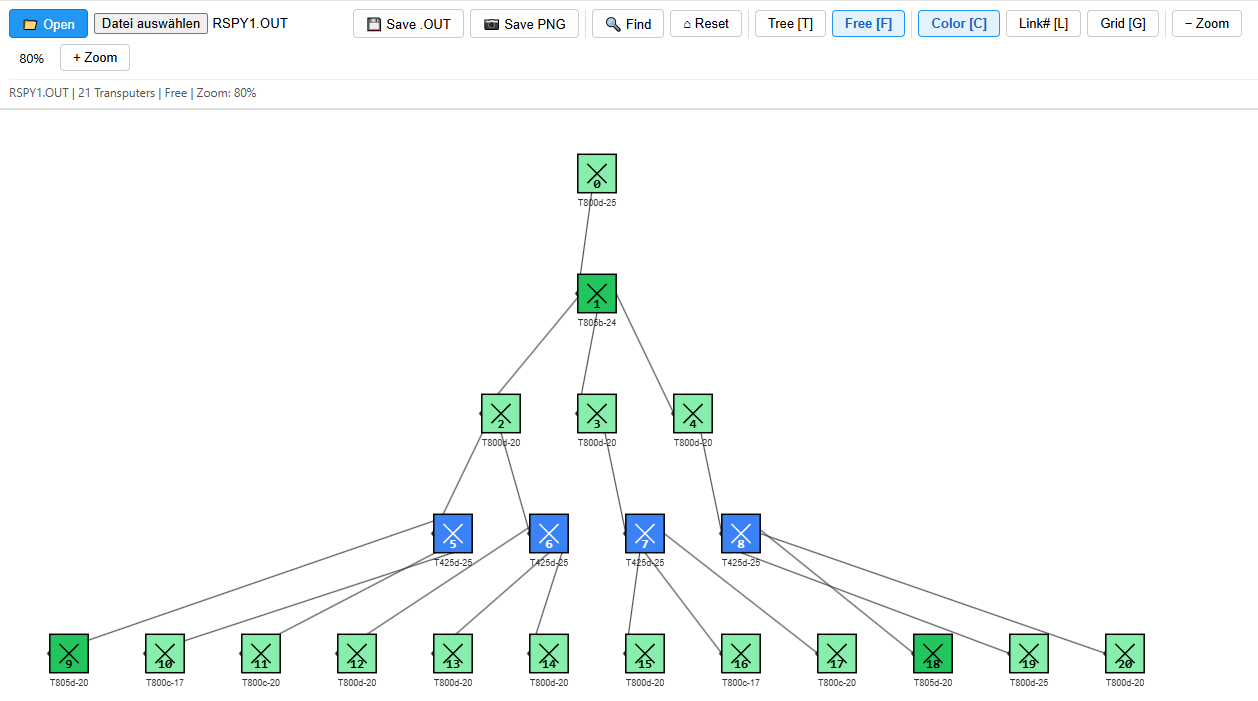
Because a tree view does not make sense all the time, think matrixes or torus’s… so you can switch to the Free view, in which you can move the Transputer nodes at will.
When you Save the .OUT file (which will do a simple download), the icon coordinates will be added to the .OUT file and will be used when you load the file later.
You can toggle these features:

  • Colo(u)r will paint the Icons by type (T414, T425, T800, T805)
  • Grid will enable a grid to make your sorting look tidier
  • Link # will add the link numbers to the connecting lines
  • and Reset will restore your mess to what the file(-design) looked at load time.

Just click here to start TNV in a new browser window.

iTest

This is a simple DOS tool I’ve written to scan a system for a link-interface (aka C011/012). Similarly to the standard tool ‘ispy’,itest just does a scan on a given port address (default is 0x150) and tries to identify a device behind it (16 or 32 bit Transputer, C004).
Depending on the result, a clear text info and a (DOS) error code is returned, which could be used in a batch file. A sample batch file for scanning the usual ports is included in the archive as well as the source (Turbo-C[++]).

Download itest here

PePo

“PePo” is my very, very simple DOS Peek/Poke Tool, to have a quick look into a Transputers RAM. Actually it can be used with any B004 compatible interface which supports the INMOS protocol.
So it also works fine with the NumberSmasher i860, which is the reason, why it insists on a 32bit alignment. It uses the Port Address of 0x150 by default. Define the environment variable “TRANSPUTER” to change this.
Usage is simple: Just call PePo with either “peek” or “poke” and an address you want to read/write from/to, so to read the first five 32bit lines in a Transputers external RAM enter:
 pepo peek 80001000 5
To write something to it enter
 pepo poke 800010000 deadc0de

Download PePo here

Inmos MMS2 archive

To make things easier configuring your C004 network, I prepared an archive for instant use.
It contains some example soft- and hardwire files, an ISERVER.EXE (the program you need to upload code into your Transputer) as well as a batch file to easily start MMS (RUN_MMS.BAT).
Also you will find a folder with INMOS’ pimped version of ANSI.SYS called BANSI (“Better ANSI”), because all INMOS tools make heavy use of ANSI screen control. So put that into your CONFIG.SYS.

Download the MMS2 archive here

The Transputer Tool Kit (TTK)

This is a collection I’ve put together, providing all essential tools to get you started with your brand new/old Transputer equipment. Read this post to learn more about its contents.

Download the TTK archive here

The Transputer SDK

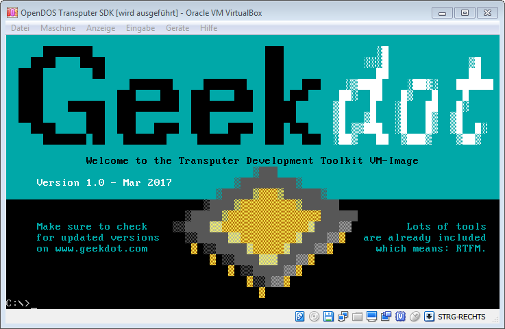
For a start, I’ve prepared an “Transputer SDK”, well, actually it’s a FreeDOS VM image for VirtualBox containing some of the most commonly used cross-compilers and Transputer software, so you don’t need a Transputer running to host a compiler:

  • INMOS Occam
    • version D7305  (more DOS oriented)
    • and D7405 (comes with many cool optional Windows tools. Windows is not provided.)
  • INMOS C (version D7414)
  • LSC (versions of  ’89 and ’91)

Download the image here.

Documentation for all these compilers are available at the usual place.
AFAIK there’s no complete documentation of all additional features of the D7405 package – a 28 page ‘flyer’ from ST can be found here.

Additionally you’ll find the sources for the occam Mandelbrot demo used for the Apple IIgs, as well as my beloved “Mandel” tool, which runs on DOS only.
Both can be fully compiled in the VM (Borland C is provided, too).

Small Howto:

When using one of the INMOS compilers, you have to set some environment variables first. To do so, execute the batch file inside the corresponding folder.
For example: You want to use the D7305 occam compiler (which I recommend for the first steps) – change into its folder

C: > cd D7305A

and call the identically named batch-file

C:\D7305A > D7305A.BAT   (hint: FreeDOS has auto-completion, so enter “D” and hit TAB)

This sets all paths etc. and you’re good to go. Change into the OCCMANDEL folder, call the make_t8.bat batch and let the magic happen 😉 The binary will placed into the \bin folder.

The DOS “Mandel” program requires a PC with a B004 Transputer interface – but I’ve added it for completeness. To compile it, just call the included nmake inside the DOSMANDEL folder.
It’s a very good example for mixed code, as it uses the LSC C-compiler as well as Borland C.

So have fun fooling around. I know, it’s a steep learning curve, but as soon you dive deep enough into Transputer matters, you’ll be amazed and will ask “why the heck did this technology never made it?!?!

Paradico – “The cube”

This is yet another pretty unknown Transputer module. The silkscreen print says “PARADICO – beheer submodule – BOP 1990”. Well, beheer is Dutch for management, so it was the management submodule for… something.

I got myself 4 of those from my Transputer-Bro’ Mike and after a good year of lying in my cupboard it was overdue to do something with them.
Mike was kind enough to do the basic deciphering of all the traces, links and stuff, so it was basically just building & wireing a front- and back-plane to get them working.

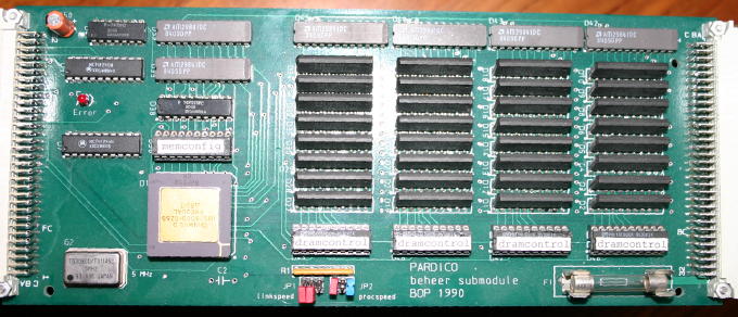
This is how one PARADICO looks like:

Paradico

Not everthing is readable here but it does the job because the PARADICO is a pretty standard Transputer design. More or less a huge TRAM. So nothing fancy about it:

  • One T800-25 Transputer
  • 4MB DRAM (4×256)
  • Some PALs for the memory decoding
  • Buffers for the links
  • A 5MHz oscillator
  • A fuse… just to be safe 😉
  • Handy jumpers for LinkSpeed and CPUSpeed

IMHO this is actually quite a waste of space but in these days you have to take what you get, right? 😉

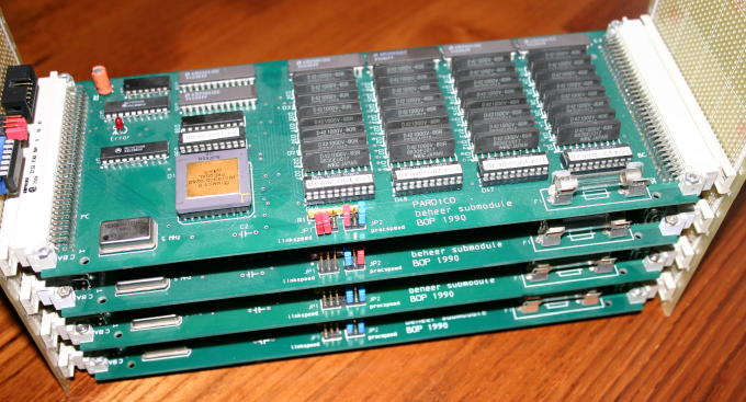
Ok, so I ordered 8 DIN41612 sockets and after a day worth of soldering “The Cube” was finished:

4paradicos

“The Cube? It’s not square at all!” you might say. Yes, true, but the specs are all nicely squared so here’s the proof. The Cube has: 2² Transputers running at 5² Mhz, each has its own 2²MB RAM. Voilà, a cube 😉
For the convenience of connecting the cube to more or less any other system, I’ve added a hex-inverter so notAnalyse, notReset & notError can be converted into their “positive” counterparts (in the upper left corner of the picture, next to 3 red jumpers).

This is the ispy output connected to the “Gerlach Card“:

Using 150 ispy 3.23 | mtest 3.22
# Part rate Link# [  Link0  Link1  Link2  Link3 ] RAM,cycle
0 T800d-24 240k 0 [   HOST    1:0    …    … ] 4K,1 1024K,3;
1 T800d-25 1.8M 0 [    0:1    2:0    3:0    4:0 ] 4K,1 4096K,4;
2 T800d-25 1.8M 0 [    1:1    …    …    … ] 4K,1 4096K,4;
3 T800d-24 1.8M 0 [    1:2    …    …    … ] 4K,1 4096K,4;
4 T800d-24 1.8M 0 [    1:3    …    …    … ] 4K,1 4096K,4;

And if you happen to stumble over a Pradico yourself, here’s the pinout of the front  DIN41612 connectors:

          X  A32 C32   X
        GND  A31 C31  GND
 UpNotError  A30 C30  DownNotError
 UpNotAnaly  A29 C29  DownNotAnaly
 UpNotReset  A28 C28  DownNotError
        GND  A27 C27  GND
         X   A26 C26   X
   LinkOut0  A25 C25  LinkOut1
    LinkIn0  A24 C24  LinkIn1
        GND  A23 C23  GND
        GND  A22 C22  GND
         X   A21 C21   X
   LinkOut2  A20 C20  LinkOut3
    LinkIn2  A19 C19  LinkIn3
        GND  A18 C18  GND
         X   A17 C17   X
        GND  A16 C16  VCC
        GND  A15 C15  VCC
         X   A14 C14   X
         X   A13 C13   X
         X   A12 C12   X

JP1:
1 LinkSpecial
2 Link0Special
3 Link123Special

JP2:
1 ProcSpeedSel0
2 ProcSpeedSel1
3 ProcSpeedSel2

Next up: The Cube moves into the Tower of Power… when other more important things are done.

Caplin Cybernetics i860/Transputer cards

Caplin Cybernetics (just Caplin for short) was one of those many UK based (London to be exact) companies building Transputer based high-performance systems. Caplin seemed to be specifically concentrating on providing Transputer technology for DEC systems, namely VAXen.

As of now, I do not know much more about Caplin, but I know there are still some former employees around and I’d be happy to learn more about the company as well as the systems I’m going to describe further down.

By a lucky indecent I got my little greedy hands onto 2 different Caplin systems. Both connecting Transputer (networks) to a mighty Intel 80860XP.
While these boards have i860’s on them I’ve put them into this Transputer category, as they were meant as math accelerator for Transputer networks, not the other way round like the DSM860 boards, which used Transputers mainly for networking.

I don’t have any documentation for those boards but I hope to get them working as soon I figured out how to connect to the Transputers, find out more about the memory-mapping and found a way how to read those damn Bipolar-PROMs.

That said, from here everything is just wild speculation, assumption and finger-in-the-air-guessing – If you know more/better: Let me know please!

I’m specifically looking for the document called “Caplin XPR Series Technical Overview”. If you still have a copy or you do know somebody who might: I’d be very happy to hear from you!

HXI860

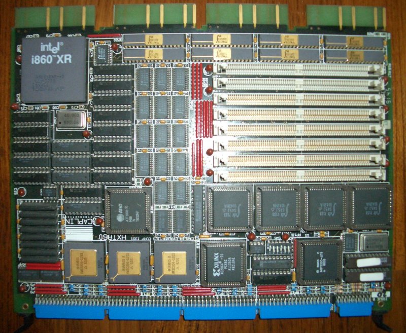
The HXI860 seems to be the earlier implementation of a Transputer-to-i860 board. It is a quite late i860 implementation though, featuring the first incarnation of the i860, the 860XR, predecessor  of the 860XP.

A picture says more than a 1000 words: The HXI860 in full view

HXI860-total

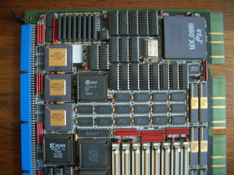
Let’s start with the left side of the board. The picture is a bit blurry (sorry) but it’s enough to identify what I’m going to talk about:

HXI860-upper

Starting on the left there are many blue 2-row pin connectors. This seems like a job for long winter evenings to find out which pin is connecting to what.
Then there are the 3 “golden boys” next to the connectors: From top down those are 1 T800-25 and two C004 linkswitches. Above the T800 there’s 4MB for his own use.
Then there are two FPGAs, one with the AT&T logo (ATT3020) and one more familiar XILINX XC2064, both getting their programming from an Xilinx 1736A PROM.
In the top-right corner the heavy-wight-champion i860XR (40MHz) surrounded by lots of buffers and GALs. The long DIP ICs on the right edge are IDT73210 octal transceivers with parity checking.
Rightmost are the connectors to the DEC Q-Bus… luckily only power & GND are taken from there, so you don’t necessarily need a VAX to use the board.

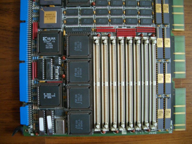
The right side of the board looks like this:

HXI860-lower

Ignoring the lurking C004 and Xilinx CPLD the leftmost black square IC is an T222C-17 which most likely controls the initial C004 configuration. He gets his code from two ICT 27CX642 which are quite strange devices: Made like CMOS EPROMS they use differential memory cell techniques to provide bipolar-prom speed. No idea how I will be able to read them out with my standard EPROM programmer.
Also, there’s a “6bit” dip-switch next to the T222 which I was told will be used to configure the link routing… let’s see what I will figure out by try’n’error.
The other four square ICs are 2Kx16 dual-ported RAMs (IDT7133). Four of them makes 64bit… well, that the i860 memory bus interface.
Last but not least there’s a long DIP IC above the DP-RAM… it’s an C012 Transputer link-adapter. So one Transputer link must be connected here, converted into 8-bit parallel. Could it be that they connected the 64-Bit RAM of the i860 via a transputer-link? (shudder)
Ok, and obviously there are 8 SIMM slots for i860 RAM… parity RAM required.

XPR201

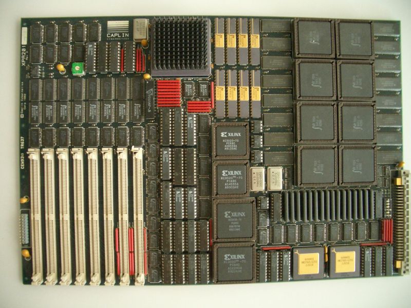
This much bigger board seems to be the successor to the HXI860 and I was told it was the fastest i860 board Intel ever tested. Also this seems to be a prototype and was never officially sold.
It now features a 50MHz i860XP (fastest i860 available), two instead of one T800 but no C004 at all. Also the communication between the Transputer(s) and the i860 seems to be fully memory-mapped and no C012 is involved.

Here’s the full-view:

XPR201-total

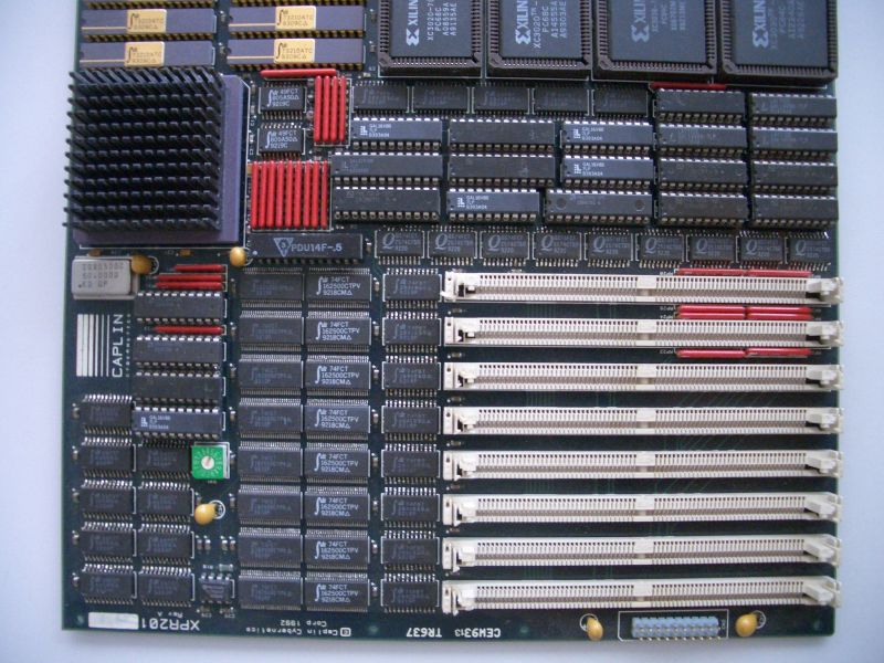
Let’s go into detail… the “Transputer side” for a start:

XPR201-T800side

The connector at the top-right edge is yet of unknown type.
Below this, there are 2 T805-25, each having 4MB of RAM. Two AM27S33 4Kx4 bipolar PROMs (flanking the RAM to each side) seem to offer the 4K boot-code.
This board, too, has a 6bit dip-switch. Again, no idea yet what it does.

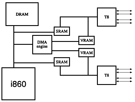
The most space in this picture is used by the much more sophisticated i860-to-Transputer interface, which is so complicated that it needs a diagram for itself (Thanks to Mike B. for beautifying this!):

XPR201

Eight(!) 4Kx16 IDT7024 dual-ported SRAMs are used to convert the i860’s 64bit bus to the Transputer 32bit bus – most likely they’re part of the “DMA engine”, too.

For doing this you normally only need 4 of them, but as you can see on the above diagram, Caplin chose to use the two T800 independently, so each Transputer has his own 16k SRAM directly connected to the i860.
Then, each Transputer is also connected to a 1MB VRAM bank (consisting of eight HM538123 having 128K word x8 DRAM and 256-word x8 Serial RAM). I was told the serial-side is connected to the Transputer, the parallel-side to the i860. Behind the VRAM is the “DMA engine” most likely the array of XILINX FPGAs you can see on the upper edge of the picture below.

The reason for this “over engineered” design most likely was, that you could use the SRAM for small but very fast read/write operations, while you would use the VRAM for bigger chunks of data.

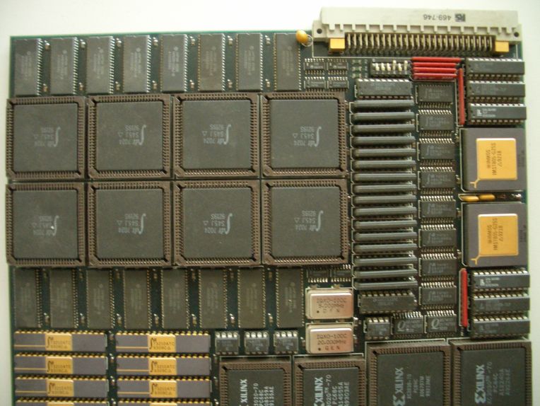
The lower-edge (“i860 side”) overlaps a bit with the above picture of the “Transputer side”:

XPR201-i860side

Again, like on the HXI860, lots of IDT73210 octal transceivers, the 4 XILINX FPGAs (the “DMA-engine”, also fed by 1736As) and a huge array of GAL/PALs doing the bus-handling.
Then there’s the i860XP (50MHz) hidden under a heatsink.
A bit below is a 16-positions dial – no idea what it does. First thing coming to my mind: RAM timing.
Finally even more buffers connected to 8 SIMM slots (the i860 private RAM, Parity-only again).
The blue connector on the bottom edge is meant to connect to a 2 digit, 7 segment display which I have on a second board I own.

Intel EISA Chipset

This chipset started it all… it was the first EISA chipset produced and the one which riddled me the most. Mainly because I have two EISA boards behaving differently when it comes to expansion cards which were developed later (~1992-94) and so I suspected the Bus Controller to be the reason for all the hassle:

The Hauppauge 4860, an early EISA system and my Intel Professional Workstation (aka LP486, not yet documented on this page).
The first is using a 82350 chipset while the latter has a 82350DT. Where’s the difference? There’s no clear answer to this anywhere, so I had to do some lenghty, in-depth research.
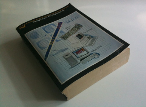
Good that I do not only collect ancient cool hardware but also some documentation, e.g. the 2″ thick Intel “Peripheral Components” handbook from 1991…

Intel_Periph

Here’s my conclusion:

The ‘original’ 82350 Chipset -released May 1990- included just 2-3 chips: 82357, 82358(-33) and (optionally) 82352.
The 82350DT -released April 1991- consisted on 5-7 chips: 82357, 82358DT, 82359, 82351, 82352, 82353 (some of them used multiple times).
The difference between the non-DT and DT version of the 82358 seems to be the synchronous interface to the 82359 DRAM controller, which wasn’t available in the initial chipset.

Chip-by-chip round-up of the chipset:

The 82350DT EISA chip set contains 7 VLSI chips to build a complete EISA
system. It is built upon the 82350 EISA chip set utilizing the 82358DT EBC and
82357 ISP and then adds VLSI components:

  • 82359 DRAM controller.
  • 82353 Advanced Data Path,
  • and 82351 LIOE Local IO Peripheral

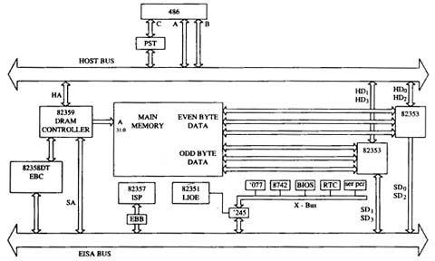
The picture below shows a 486 based system with 82350DT chip set.

illu

The host bus connects the CPU and the memory subsystem. Tlte peripheral bus (X-bus) is an 8-bit bus to support the motherboard IO functions: keyboard, floppy and the LIOE which integrates the parallel port; and support: extemal teal time clock und serial ports. The peripheral bus is a buffered version of the 8-bit ISA bus. The memory subsection operates independent of the CPU clock. This independence is accomplished through the use of 82359’s integrated programmable delay line and the  rogrammable state tracker(PST) function. The integrated programmable delay line is used to time precisely the DRAM cycle sequence to DRAM parameters. The PST resides cm the CPU module. Tite 82359/82353 reside on the motherboard. They are indifferent to the CPU/cache used. The PST converts processor cycles to a form acceptable to the 81359. This allows different CPU/ cache combinations to be connected to the same motherboard. Further, it translates CPU’s clock-dependent handshake to clock-less memory interface handshake.

Local I/O EISA Support Peripheral, lntel 82351

The 82351 supports or integrates all of the IO peripheral functions for a typical EISA system board with a minimum of external logic. lt integrates local I/O ddress decoder, EISA system configuration registers, two external serial I/O ontroller interfaces with four assignable interrupts generation, external EISA onfiguration RAM interface, parallel port interface, external floppy disk controller Interface, external keyboard (8×42) controller interface including interrupt generation, and external real time clock interface and EPROM or FLASH EPROM BIOS ROM interface. lt was available in a 132-pin PQFP (Plastic Quad Flat Pack) package.

EISA Bus Buffer (EBB), Intel 82352

The 82352 is a bus buffer IC for EISA bus system. Three 82352 chips are used in a 82350 EISA system. Only one 82352 chip is used in a 82350DT EISA system.
lt operates in three modes. ln Mode 0 it performs data latch and swap functions.
It allows swapping and assembly of  data between the host and EISA/ISA buses on a byte by byte basis. In Mode 1 it provides 1 buffered path between the host data bus and DRAM with parity generation/check. Mode 2 was reserved by Intel for future use (never happened). Mode 3 provides address latching function between the host and EISA/ISA buses. The 82352 was available in 120-pin quad flat pack (QFP).

Advanced Data Path, Intel 82353

The 82353 provides advanced data path in e 82350DT EISA bus system. Two 82353 chips are used in a 82350DT EISA bus system as showed in the graph. Each 82353 is designed as a 16-bit slice. Two 82353 chips can provide parallel interface to 32, 64 or 128- bit wide memory structures to a 32-bit host and system bus.
The 82353 provides optimal 486 burst performance. Each memory cycle enerated by the address controller chip causes 128 bits of memory data to be latched in two 82353 chips. Once data is latched, these 82353 chips mux the four dwords to the destination in one wait state. The 82350DT EISA bus has 128-bit memory bus. A typical burst is 128-bit wide. and a bus with the same width
allows to read the whole burst in one memory cycle. This provides a zero wait state burst at any frequency. The 82353 was available in a 164-pin PQFP package.

Integrated System Peripheral (ISP), Intel 82357

The 82357 contains DMA controllers, interrupt controllers and programmable 16-bit counter/timers. lt provides high-performance arbitration for CPU, EISA/ISA bus masters, DMA channels and refresh. It also provides logic for generation/control non-maskable interrupts. The DMA function is provided by two inbuit 82C37A DMA controllers. These DMA controllers are connected in cascade mode to provide seven independent programmable channels. The timing control for 8-, 16- and 32-bit DMA data transfer is provided. The data transfer rate is 33MB/sec. There are two 82C59A interrupt controllers in the 82357 chip, which provide 14 independent programmable channels for level or edge-triggered interrupts. The 82357 contains five 82C54 compatible programmable 16-bit timers/counters. lt was available in a 132-pin PQFP package.

EISA Bus Controller, Intel 82358DT

The 825358DT provides an interface between 386/486 CPU and EISA bus system.
It provides EISA/ISA bus cycle compatibility with the host(CPU) bus. The 82358DT is a part of intel 82350 and 82350DT chip set. It translates host(CPU) and 82359(DRAM controller) cycles to EISA/ISA bus cycles. lt supports 8-, 16- or 32-bit DMA cycles. lt also supports host and EISA/ISA refresh cycles. lt generates control signals for advanced data path(82353) and EISA bus buffer(82351). lt was available in a 132-pin PQFP package.

DRAM Controller, lntel 82359

The 82359 is a highly integrated advanced memory controller. lt supports 386 and 486 microprocessors. Its operation is independent of speed and type of the CPU. It allows a system designer to implement a variety of CPU/cache combinations. It provides address control, refresh generation and critical DRAM timing generation. In conjunction with two advanced data path devices (82353), it acts as a highly integrated 32-bit dual ported memory controller. Its two ports (or address gateways) to main memory are: one exclusively for the host and one exclusively for EISA. This configuration of ports permits CPU activity to be isolated from EISA bus activity. It controls up to 256MB of motherboard DRAM. It supports 32-, 64- or 128-bit wide memory configurations. lt was available in a 196-pin PQFP package.

Bus Master Interface Controller, Intel 82355

The 82355 is used in an EISA add-in card (expansion board) – thus rarely found on mainboards.
It supports 16- and 32-bit burst transfers at maximum data transfer rate of 33MB/s. It also supports 32-bit non-burst and mismatched data size transfers. It automatically handles misaligned double-word data transfer with no performance penalty. It has two independent data transfer channels with 24-byte FIFOs. Expansion board timing and EISA timing operate asynchronously. The 82355 supports 32-bit EISA addressability (4GB). It integrates three interfaces:
EISA, local CPU and transfer buffer. It supports automatic handling of complete EISA bus master protocol. This includes EISA arbitration/preemption, cycle timing and execution, byte alignment, etc. Further, the 82355 supports local data transfer protocol similar to traditional DMA. It was available in a 132-pin JEDEC PQFP package.

The EISA Bus

Actually I have no idea why this subject caught my interest so well.
During the hey-days of the EISA bus I wasn’t interested at all, thought that’s something which will never take off and was intended for servers only. I happily stuck to clumsy ISA and sat there until PCI was affordable (ASUS SP3G anyone?).

Now, fiddling with all those exotic cool mainboards, EISA crosses my path all the time. The way EISA is configured, the somewhat cumbersome use of cf.exe (ECU – EISA Configuration Utility) tool drew my interest… maybe because it has the scent of manliness 😉

In my humble opinion, EISA was a crutch, but it layed some basics for the next 10 years:

  • It defined (as a by-product) a standard for the ISA bus, which was all chaotic before
  • It forced Big-Blue (IBM) to think over their Microchannel licensing
  • It was a test-bed for how do things right… later known as PCI

That said, it is the fun twilight-zone between ISA’s direct access “do what you like” and PCI’s “you touch – you die” approach. Where else do you have 32-bit speed and can still change bits manually with DOS’ debug?

Hacking the AVM T1

AVMT1Press

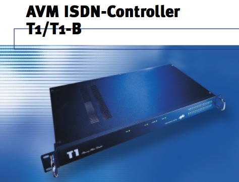
It was inevitable… the biggest system AVM built was the “T1”, a 30 channel ISDN controller in a sleek 1U 19 inch case of which nothing more than the above marketing picture seems to exist.
One fine day I had to had one – and today is the day!

I was able to find a AVM T1 on ePay which was not very well advertised so I had no “professional competition”. Even I didn’t spent a fortune it was a bit of gambling because I didn’t knew what to expect.
Besides AVMs own T1 PDF manual there’s next to nothing available in the Web – So this section is yet another WWW-exclusive brought to you by geekdot.com 😉 (Ok since 2009 others discovered this page and also this cheap entry into the wonderful world of multi Transputing)
Still, the docs said “a Transputer network with 9MB RAM” so I couldn’t go completely wrong. That said, I was expecting SMD T400s at AVMs usual sluggish speed…

First look

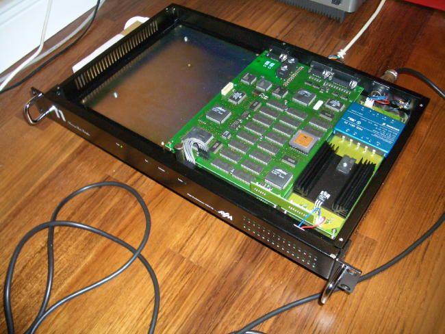
When the box arrived first thing was getting out good ol’ screwdriver and open the case…

AVMT1open

…and I was very surprised:

  1. A socketed T425 – so that’s another easy upgrade then.
  2. An external power supply (48V)! That’s strange but also neat – no noise and next to no heat in the case itself
  3. Also, the board is very small…  lot’s of room left in the case.

That’s done by intention as you could buy the T1-B, where “B” stands for the “Booster Board”, yet another board with 4 more Transputers and another 8MB of RAM giving a total of 7 Transputers and 17 Megs of memory. Quite a setup for just an ISDN controller.

Sniffing around

Ok, this beast has to do something better than handling 30 boring B-Channels… Mandelbrot for example 😉 So let’s see how this thing is/was supposed to speak to the outside world.

The manual is talking about an ISA or PCI controller-card which will be connected to a 9-pin Sub-D connector. Having a closer look to the mainboard where that connector is seated I discovered some other old friends: AM26C31 and AM26C32.
Aaaaalrighty, RS422 time… that’s the same way my Tower of Power is transmitting its data. So I can use my TTL-to-RS422-converter I’ve built for the Gerlach card.

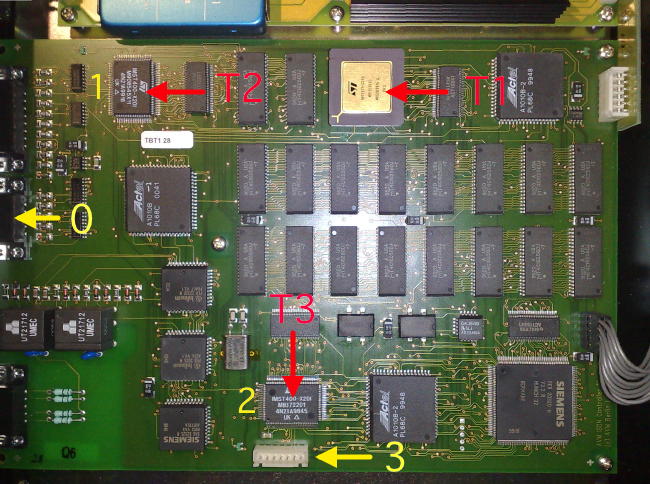
Out goes the multimeter and after a while I figured out the the traces on the board. For a better understanding, here’s the “map”:

AVMT1Board

Marked by the red arrows are the three Transputers:  T1, a T425-25, is the “application processor” while T2 and T3 are more simple T400-20 handling the ISDN subsystem.

The yellow arrows mark the four links of the T425 – which is probably the reason why AVM used a 425 vs. their usual T400: this time they really needed 4 links.
Link0 is connected to the 9-pin sub-D connector (via the RS-422 transmitters/receiver) for interfacing to the PC.
Link1 and Link2 are directly connected to the T400s.
Link3 goes to the connector on the lower edge of the board. I bet this is where the “booster board” would be connected… not a hard bet, I admit.

The pinout for the 9-pin sub-D connector (female) is:

 1 Link0-IN -
 2 N/C
 3 Reset-IN +
 4 N/C
 5 Link0-OUT +
 6 Link0-IN +
 7 Reset-IN -
 8 GND
 9 Link0-OUT -

As Link0-IN and Reset-IN are routed through two separate 26c32 I assume there might be more differential signals available. If time allows I’ll dig deeper on this matter.

Do something Gromit!

Well then… a cable was built in a couple of minutes – some cursing and swearing about the differential polarity and then the exciting moment came: Let’s see if it’s really so easy again!

It is! And here’s the ispy output for the T1 (connected to the “Gerlach card”):

Using 150 ispy 3.23 | mtest 3.22
# Part rate Link# [  Link0  Link1  Link2  Link3 ] RAM,cycle
0 T800d-25 288k 0 [   HOST    …    …    1:0 ] 4K,1 1024K,3;
1 T425c-20 1.6M 0 [    0:3    2:0    3:0    … ] 4K,1 4092K,3.
2 T400c-20 1.7M 0 [    1:1    …    …    … ] 2K,1 1022K,3.
3 T400c-20 1.8M 0 [    1:2    …    …    … ] 2K,1 4094K,3.

Some remarks about this:

  • 9 MB is true. The “application processor” (T1) got 4MB while the two T400s got 1 (T2) and 4 MB (T3, obviously connected to the SIEMENS Munich32 Über-ISDN controller).
  • While the built-in T425 is spec’ed for 25Mhz it’s just running at 20MHz… what a waste of bang… and what an opportunity for improvement :->
  • The linkspeed is at maximum… which one would expect with directly connected links. But with AVM you’ll never know 😉
  • The RAM-speed is pretty good (compared to what they did to the B1) – even they just used 70ns RAM.

Next up: Having fun with Mandelbrot! Having just T4xx Transputers it can only use the integer algorithms (i.e. no floating point) but who cares for a quick start?!

It’s working and showed another nice gadget: LEDs! Each Transputer has a tiny SMD-LED connected to it’s Link-Out.
So having the T1 underneath the table I have quite a nice light-show while the three are working their a** off 😉

If you happen to have no access to a RS422 converter: Never say die!
Like said above, there’s still Link3 available – normally meant for the booster-board – and it’s pure TTL. All you need is a somewhat non-standard plug to this connector. Be creative but don’t forget that unbuffered link connections only allow a distance of a couple of inches/centimeters!

The pin-out (so far) is, counting from left to right:

 1 - 5V VCC
 2 - T1 Link3 OUT
 3 - T1 Link3 IN
 4 - RESET
 5 - T3 Link1 OUT
 6 - T3 Link1 IN
 7 - GND

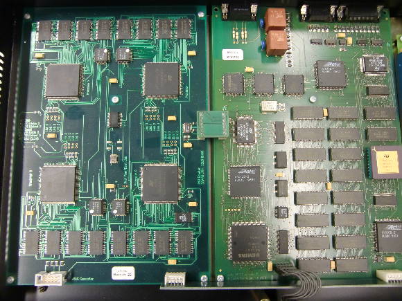
[UPDATE 11/14/10] Again, with some ePay-Luck I got another T1… and it again was some kind of lottery… and I had luck! This time it’s a T1-B!! This means, the “booster board” is installed. So opening the case, it looks like this. On the right the normal T1-board, to the left, “da mighty booster board” 😉 I’ll call it “BB” from here…T1-Booster-Full

As expected, it’s connected via Link-3 of the T1 Board. On the lower edge of the picture you can spot the power-supply “module”. It’s longer than in the T1 configuration and provides 3.3V/GND to the BB, i.e. the BB is 3.3v only!!

Here’s the BB alone:

T1-Booster-Board

All in all the BB is more modern than the T1-board. Very suspicious are the JTAG connector on the lower left having its lines connected to a EEPROM (AT28V256, right edge of the BB board, above the row of RAMs). Further up, left to the CPU nearby is a pad with the lable “Boot from ROM/Link”. I wonder what the default is and what’s inside that EEPROM – will investigate later.

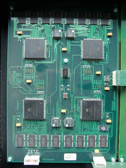
Most importantly the BB board features 4 ST20450 processors, which aren’t INMOS products anymore. They were designed by ST after they bought INMOS. For short, the ST20450 is a T425 on steroids. More on-chip RAM (16K), higher clocking (40MHz) and some more instructions.
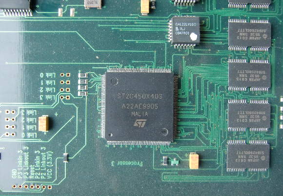
Each ST20450 has its own 2MB of RAM and a GAL handling the memory etc.. Here’s a close-up of a single ST20450 “module”:

T1-Booster-1of4

Mind the careful markings/labels on the board. The CPUs are numbered (“Processor 3”) and there are pads for Links etc.

Finally, I currently have no tools to check/use ST20450 processors. ispy finds the Transputers on the T1 board but freaks-out when it pings the ST20s.

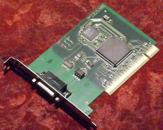
Here’s another new addition: A picture of the official T1-PCI interface. It contains a PCI-controller (the big IC) and a XILINX FPGA… probably containing a synthesized C011.

T1_Interface

UPDATE:

Jonathan Schilling also plays played around with an AVM T1 on his page including the original ISA controller card… and he‘s making made very good progress!
[2015, Jonathan quit ‘the scene’ and handed over all his equipment… further on, it seems in 2020 he closed his pages]

Another UPDATE [2017]:

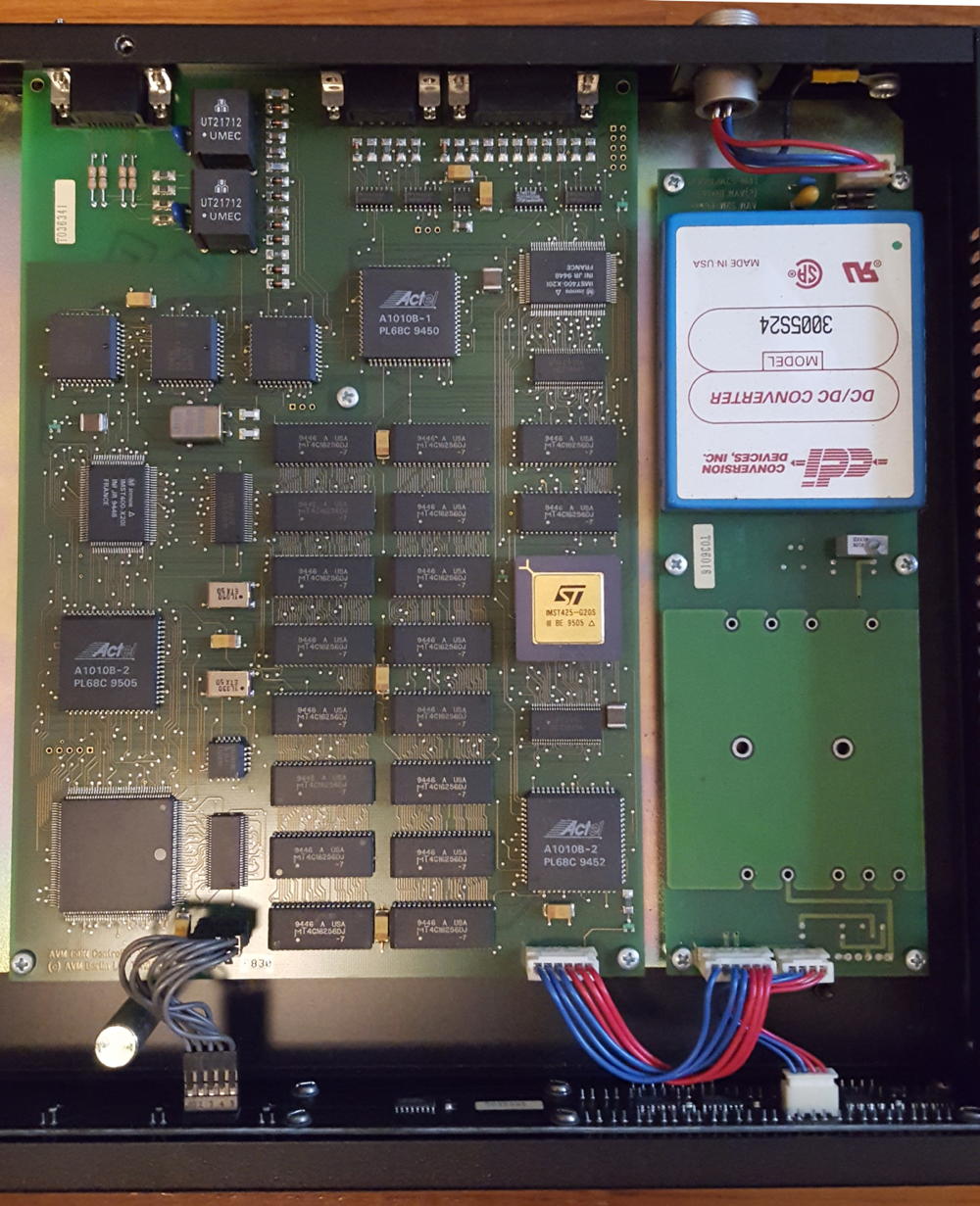
Just got another T1 off ePay… surprisingly it contained yet another board-design. I’ll call it the “non-booster layout“. This board has no connectors for the booster-board and missing the regulator below the DC/DC converter – no need for 3.3V.

TODO: 

  • Change the T425
  • Make the 30 front-panel LEDs blink
  • Figure out for what the female 15pin sub-d connector is good for (not mentioned in the manual)

Here’s how to access the LEDs at the front – thanks to Michael Brüstles research:

typedef unsigned long int u32;

/*
 *  addr XXXX-XXXX-X111-XXXX-XXXX-XXXX-XXXA-AA00
 *    
 *  wr                               0-01    __ EN __ __-__ __ __ SY
 *  wr                               0-10    08 07 06 05-04 03 02 01
 *  wr                               0-11    16 15 14 13-12 11 10 09
 *  wr                               1-00    24 23 22 21-20 19 18 17
 *  wr                               1-01    SC ST 30 29-28 27 26 25
 *
 *  rd                               0-01    readable ... content unknown
 */

int main( void ) {

    u32 *p = (u32*)0x80700000UL;

    p[ 1 ] = 0x40;  /* enable all leds 0x40 & Sync 0x01 */
    p[ 2 ] = 0x05;  /* Led01-Led08 */
    p[ 3 ] = 0x00;  /* Led09-Led16 */
    p[ 4 ] = 0x3F;  /* Led17-Led24 */
    p[ 5 ] = 0x92;  /* Led25-Led30, System, S-channel */

    return 0;
}

The DSM-860 Series

Based on a public project from Rolf-Dieter Klein and Tobias Thiel (“PC-Karte mit i860”) in the German computer magazine “mc” (2/90 to 7/90), the Munich based company DSM built several i860 boards for the PC/AT which they called the DSM-860 series.
All DSM-860 have one thing in common: They offer a high level of hardware features – no costs were feared. So naturally, those cards were not cheap. But you really got something for your money. All versions featured

  • 4 Transputerlinks for networking multiple cards
  • Connection to the hosts system-bus (ISA/EISA) via dual-ported RAM
  • A 16-bit bus is also available via dual-ported RAM on special connectors giving a throughput speed of 8MByte/s for high-speed connections between several SPC boards.
  • RAM was put on an extra RAM board making the complete SPC-860 a double-card sandwich

DSM-860

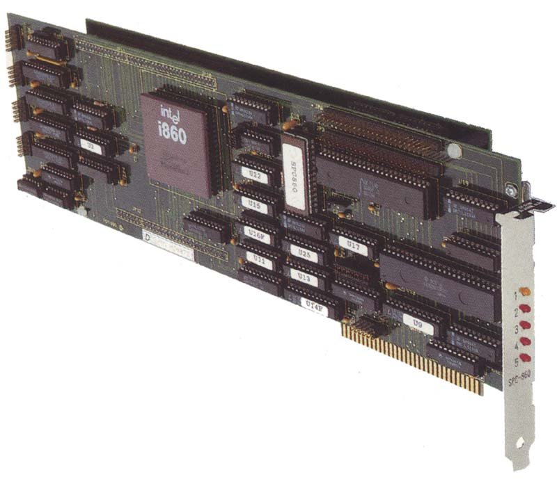
The 1st incarnation was the SPC-860, very quickly renamed to DSM-860, an 8-bit ISA card with 4MB RAM (DIL) and 4 10mbps Transputerlinks via four C012’s (polled by the i860 resulting in 740kbps linkspeed).

Here’s a picture from a 1992 ad, with separate RAM card attached:

print-DSM860-8

It did cost 16450 DM including the (GNU) C compiler and assembler.

DSM-860/16

Next, they released the DSM-860/16 (renaming the DSM-860 into DSM-860/8) being a full fledged 16-bit ISA card. It has a real Transputer (16bit T222, having its own 32K SRAM) for handling the “multiprocessor communication” and is able to support up to 256MB on a sandwiched daughter-board, now using SIMM modules instead of DIL parts.
The Hitachi HD63310 dual-ported RAM, used in the 8-bit version to communicate with the host was replaced by faster Cypress IDT7130 types (“because of the high speed of the 16-bit ISA interface” ;-)), resulting in a peak-rate of 14MByte/s.

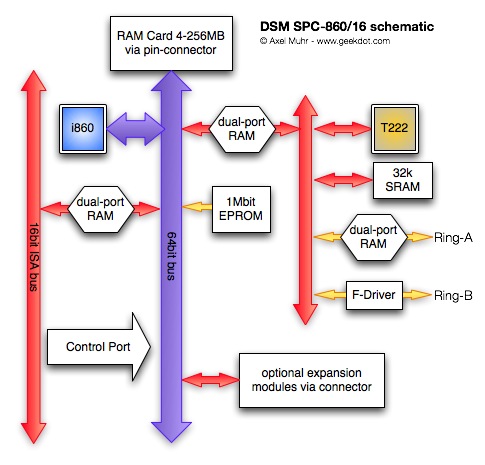
Here’s the schematic of the card and its components

SPC860schem

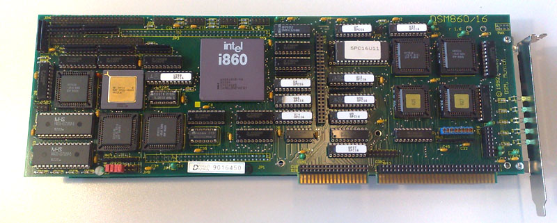
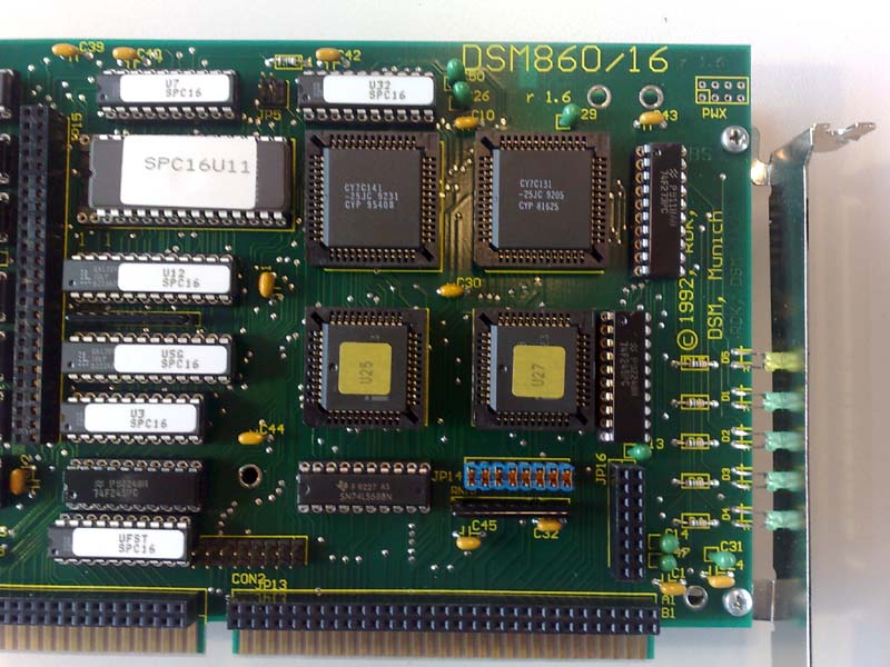
This is how it looks in reality… my DSM-860/16:

DSM860-16

As you can see, the card is not exceptionally high integrated – even built 1992 there is not a single SMD part used, everything is socketed, only some PALs could be called “custom parts”. But this does not necessarily mean it’s badly designed or build.
If you have a close look (click the picture for a bigger version), you’ll see that every part/socket/jumper on the board is nicely specified in the silk-screen printing. All GALs and the EPROM contents are available in the documentation… which has 426 pages by the way.

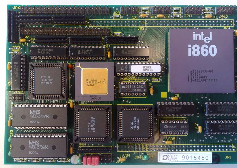
Here’s the left side in more detail:

DSM860-16_left

This end of the card is the “external comms” side. Beside the all-mighty i860 you can easily spot the golden Transputer being the communication controller.
To its left, there’s the first dual-ported RAM (1k x 8) connected to the socket for the external bus (Ring-A, located on the edge above). Below that are the two 16k SRAMs -marked MHS- for the Transputer. Then to the right are the two dual-ported RAMs (a 7C131 and a so-called slave 7C141) making the 16-bit connection to the i860’s bus. The rest of the parts are quartz oscillators (5MHz & 40MHz) and drivers/buffers for the buses. On the top edge next to the Ring-connectors you can spot the 4 Transputer links (JP9-12).

The right side is comparably boring:

DSM860-16_right

The boot EPROM, 6 GALs, again two dual-ported RAMs (this time for the ISA-bus connection) and some buffers… well, and 5 LEDs. LEDs are good. 😉
Also, you can see the pin-row connectors at the lower edge and on the left of the photo. That’s the expansion-bus. The lower connector is more or less 1:1 the ISA bus, the left one is a 16-bit bus to the i860. AFAIK, they never offered an expansion for sale.
The last (but not least) interesting thing on this picture is the copyright. Yes, it’s a DSM860/16 from 1992, RDK made it (Rolf-Dieter Klein), DSM in Munich distributed it – but it’s obviously also a rev. 1.6, which means there could be others before or after that one. If you have more informations I would be happy to learn more.

DSM860-OEM/16

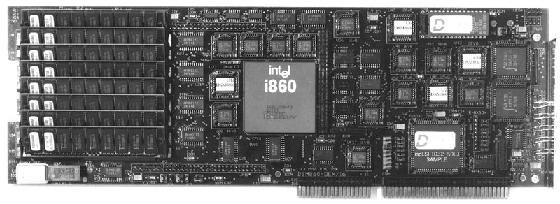
I’m pretty sure there was one more version after this rev.1.6, this b/w picture from a DSM press release about shipping the 250.000th slot-CPU card shows a very changed design. The silkscreen print says “DSM860-OEM/16”, so it’s obviously nothing for the normal market.
Mind the onboard-RAM, the missing comms-section and the high integration (SMD parts all-over) and even an early form of an FPGA from Lattice – my assumption is that this version could be the answer to the Kontron SBC860 showing nearly the same layout:

OEM_250ste
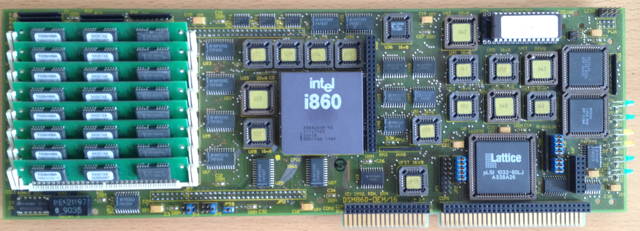
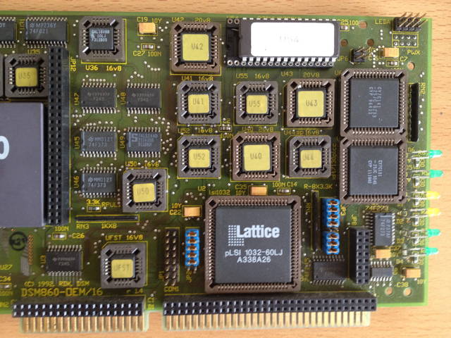
At least this ‘riddle’ is finally solved. I was able to buy an DSM860-OEM/16..Yay! As assumed, it is a modern (for 1990 standards) version of the DSM860-16 now consisting of just one board, so no more RAM card as described below- and without the Transputer and Ring-A/B stuff.

Here are my pictures of it. First of all, the card in full view:

OEM16_full

The right half shows a very high degree of integration compared to its predecessor. All DIL ICs were replaced by SMD parts and lot of logic went into PALs and even an FPGA (The contents of the EPROM is the same as with the other card, minus Transputer handling):

OEM16_right

The left half contains the CPU and the RAM. This time only 8 SIMM slots:

OEM16_left

The RAM card

DSM860-RAMcard

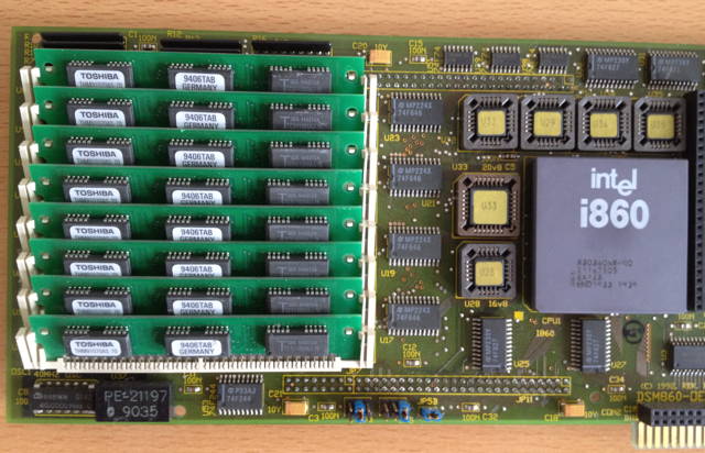
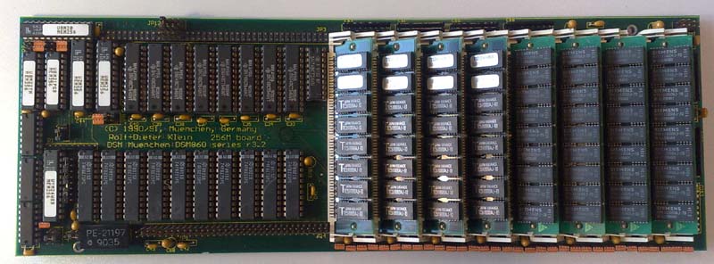
This is the 2nd part of every DSM-860 – the RAM card (except the OEM-16). Same dimensions as the SPC itself… i.e. full length. The biggest part of it is consumed by the 16 angled SIMM sockets, obviously interleaved, thus named altering slot-a & b. Only the 8 a-slots are populated on mine.
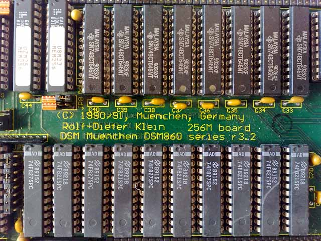
The rest of the board is used for lots of buffers and drivers, some GALs (doing the mem-mapping) and there’s quite a big copyright… again.

DSM860-RAMcard_C

One typical detail of those days is the fact that manufacturers were not very keen on having users doing upgrades themselves. Even this RAM board has standard SIMM sockets and one could simply plug in more SIMMs to expand the RAM you had to change a GAL (the one in the lower left corner with a while label saying “UXM24Wxx” on it). Obviously these GALs are the only ones notdocumented. All I know is that there were 3 GALs available differing in the last two letters of the label:

  • 8B = only a-slots can be used by either 1M or 4M SIMMs giving 8 or 32MB total
  • 16 = both a- and b-slots used with 1M SIMMs = 16MB total
  • 64 = a- and b-slots filled with 1M and/or 4M SIMMs giving 16, 40 or 64MB total.

Because the card as well as the documentation says the maximum supported amount of RAM is 256MB there might be the chance of supporting 16MB SIMMs – I did not try this yet.

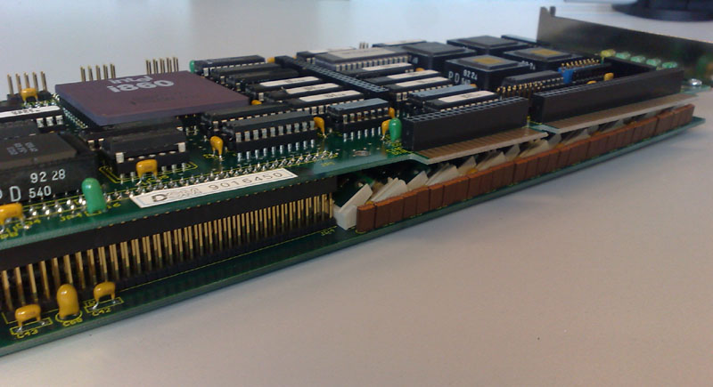
Both cards attached together give quite a big and heavy sandwich

DSM860-16_sandwich

It’s obvious that you not only need 2 full-size slots but also guide-rails inside the case to hold the weight of this beast.

DSM-860/32

This seems to be the king of the SPC hill. Technically it’s pretty much the same as the DSM-860/16 but this time featuring a 32-bit system bus – namely EISA. The EISA bus was a dead-end like IBMs Microchannel but comparably easy to implement and free of license fees.

So the main difference to the DSM-860/16 is the 32-bit wide connection to the hosts bus, visible by the 4 dual-ported RAMs used for a 32-bit wide connection to the EISA slot.

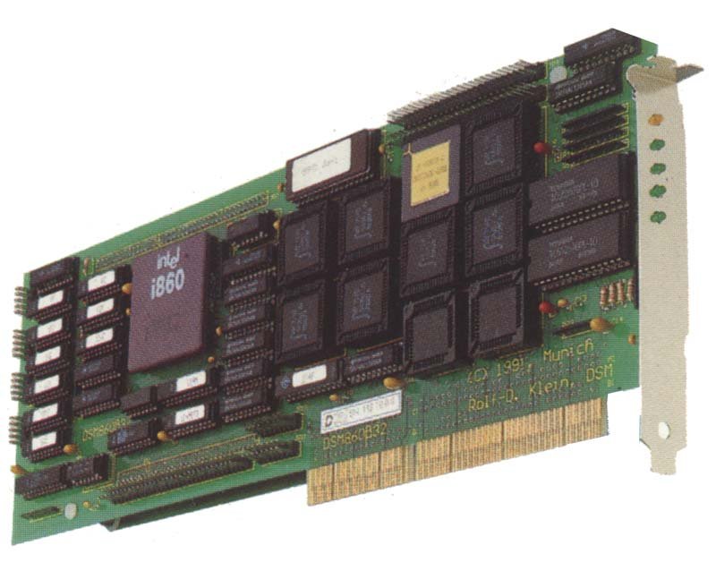
Again, here’s a 1992 magazine ad showing a probably early version of the card as the marking says “DSMß860-32” (mind the beta) and the year “1991”:

print-DSM860-32

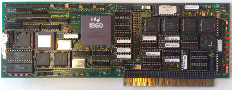
Compared to that, my version (1.2) does not look that much cluttered – also the Transputer comms part were moved to the left side of the i860 and two more LEDs were added:

DSM860-32

So the left side of the card looks pretty identical to the DSM860-16, while the right side has a bit more logic to satisfy the EISA standard, the already mentioned 2 more DP-RAMs, a bigger expansion-bus due to the EISA slot and most important: 2 more LEDs! Did I mention that LEDs are good? 😉

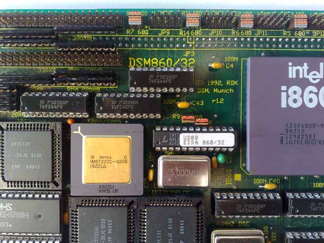
DSM860-32_C

This more detailed picture shows that the DSM860/32 was released the same year as the ISA version. This card is a rev.1.2 – again, if you know more about revisions, I’d be happy to hear from you.
You might have spotted that this card looks a bit shabby. That’s because it was pulled from some universities dumpster. It was missing some components and had some “scars”. The good thing was that none of the GALs were missing and due to the fact that every piece is documented on the card it was easy to replace the missing parts.
On the above picture you can clearly see e.g. the 100nF capacitor C40 below the i860 or the 40MHz OSC. I wish everything would be that well documented.

The Infinity card

This is a rare and mysterious beast. The documentation only touches it very briefly. It’s definitely nothing been built for the average DSM860 user – if something like that existed. For sure it was extremely expensive… and it has LEDs 😀

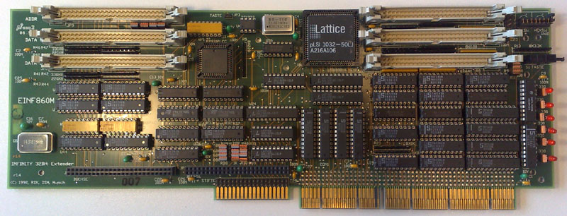
DSM-EINF860M

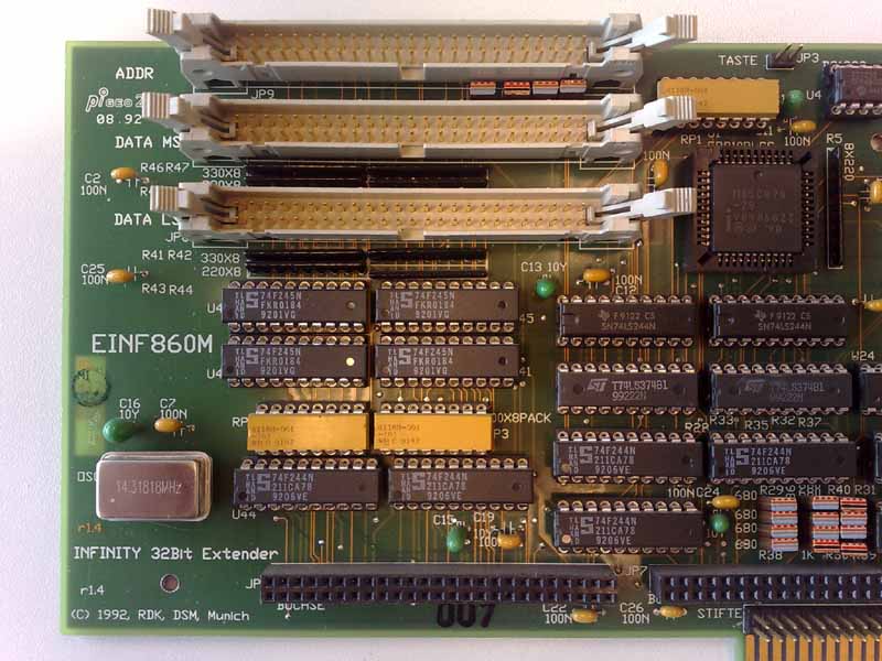
So at the first look you see 2×3 connectors for 40pin cables – the same used on the DSM860 cards (Ring-A and -B). Then there are a lot of drivers and buffers and a big Lattice pLSI 1032-50 which is a 6000 gates PLD (Programmable Logic Device). A closer look to the board gives more hints – thanks to the DSM (or RDK) habit to print as much info as possible onto the board:

DSM-EINF860M_C

Ok, first information we get is that this is a EINF860M or INFINITY 32Bit Extender. It’s like all other boards (c)1992 by DSM Munich and -as one would expect- designed by Rolf-Dieter Klein (RDK).
The three connectors are labeled ADDR(ess), DATA MSB (Most Significant Byte) and DATA LSB (Least Significant Byte).
The the right of the connectors is an Intel 85C098-20. I think that’s a One-Time-PLD, not 100% sure.

My educated guess is that this card is what the print on it says: A bus extender. Using the 16-Bit bus on the DSM860 cards one can build quite a big parallel computer. But the max. length of the flat-cable to connect each card with the next one is limited. So this card would be connected to other DSM860 cards in the same case (i.e. a 19″ case in a rack) and the extender would then “amplify” the bus-signals to be send over into the next rack full of DSM860 cards.
That said, my fear is, you’ll need two of those cards as the seperation of Adresses and Data (MSB and LSB) is nothing being used on the DSM860 cards. So my next guess is, that the INFINITY communicates over the EISA bus with the other cards and has its own external bus. Again – I’m happy if you contact me if you know more/better!

Nostalgia

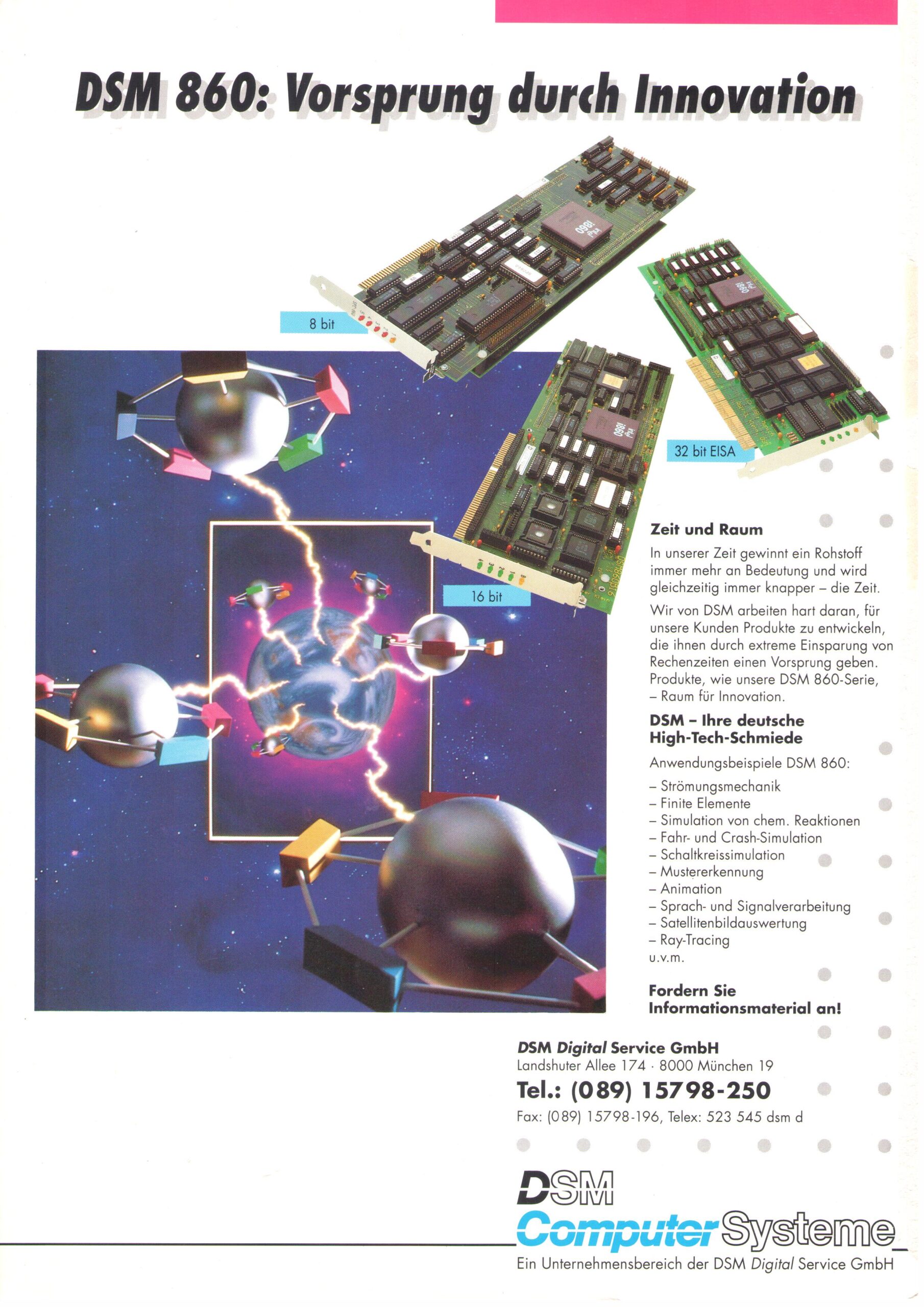
And here’s a full page ad I found in my old (German) computer magazines – it shows all 3 versions:

DSM Software

I’m in the lucky position to own the last offically released software package for the DSM860 cards.
That said, it’s a mishmash of different tools, code and compilers not always compatible with the different boards (860/8, 860/16 and 860/32). Still the sources and specifically the assembler and C compiler may be helpful for a kickstart.
I’ve adjusted the installer to create a single-install instead of the original 3 floppies installation. See the readme.txt file for more details.

Download it here.

And if you’re interested, here is the the source & binaries for my Mandelbrot example.