All posts by Axel

http://www.geekdot.com/about-me/

DesperRAM

You might have been in the same situation: Some piece of old hardware could be upgraded (aka pimped) with more RAM, but there’s no place in the world to get that type of RAM needed.

In my case it was 1Mx4 DRAM in a DIL packaging. It’s hard to come by those in a ZIP packaging – sometimes used on AMIGA RAM cards – but DIL is next to impossible.

Well, when 1Mbit RAM chips were introduced, the industry switched to SIMMs anyway… and that’s where you find those. For the DespeRAM, SOJ packaging is what you want. SOJ (sometimes also called J-Lead) means there are short pins on the IC but they’re bend inwards under the chip… pretty much like PLCC pins.

What you need for this stunt:

  • Desperation. Lots of it.
  • A hot-gun (for getting the SOJ chips off the SIMM module)
  • A fine tip on your solder-iron. Very thin solder led (e.g. 0.5mm)
  • DIL sockets for your desired piece of crap^h^h^h^h vintage hardware
  • Wire, also thin (I used 0.6mm)

Preparation:

Clean desk. Good lighting. A steady hand (no coffee or drugs – I assure you, it won’t work. I tried it ;))

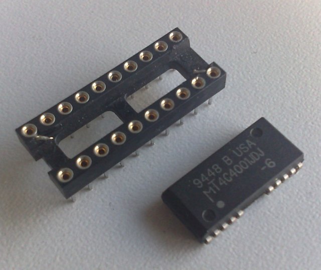
Ok, so first of all get out the hot-gun and carefully get the ICs off the module. Here’s a single chip and the socket it should be mated to

desperRAM1

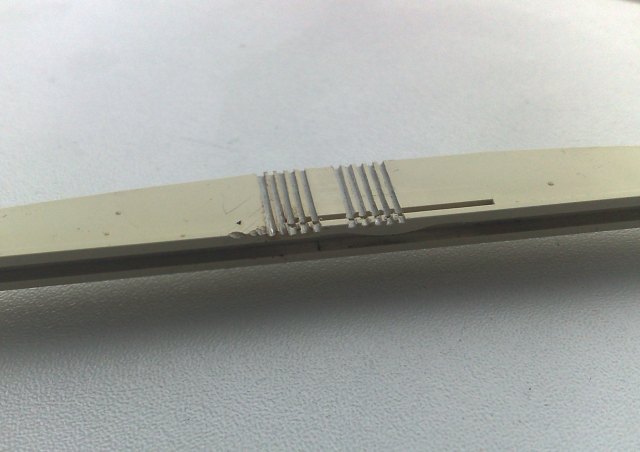
Bend the pins and straighten them. I used a needle to pry the pins upwards a bit and did the rest with tweezers. Now you have the exact spacing of the pins on your chip. Use that for building a “pin aligning tool”. I’ve used a piece of plastic and a fine saw to cut 10 grooves into it. When done, it looked like this:

desperRAMtool

Now find something on which you can fixate the chip to (still being movable). I used a block of wood and a rubber band. This worked quite well. This way, you can always adjust the position of the chip when needed.
It’s time to cut some pins. For the start I went for about an inch long – place them into your self-made tool and fix them with a piece of self-adhesive tape (Scotch in USA, Tesa over here ;)).
Now put some solder on the chip’s pins as well as on the freshly cut DIY-pins.
Carefully position your tool so that the pins do have good contact.

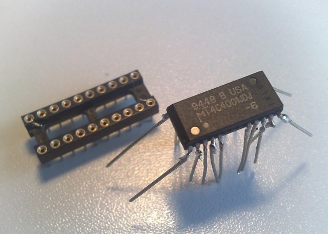
If you did everything right, a short contact with the solder iron tip should be enough to solder the new long pin to the original one. When you’re done with all pins it should look like this

desperRAM2

As you can see, I did already start to bend the new pins to fit into the socket. It’s a bit try-and-error to get the right angle. Be careful to avoid the pins touching each other or even break when being bent. Re-fitting a single pin can be a major pain in the a**!
Now you need to cut the pins into a reasonable length. First bend them into position – constantly checking against the socket. When all pins are ok – start cutting from one side to the other, bit for bit until you got the perfect length (Use the first chip as a model for others which might follow).

The seating is a bit difficult as you can’t use maximum force to push them into the socket. I used a fine caliper to actually pull the chip into the socket.

Due to the angle needed, the chip will hover quite a bit above the socket. I guess you can go lower if you go for a 90° bending – I didn’t have the patience.
Double check all connections from the original pin to the one on the socket. Also check for shorts!

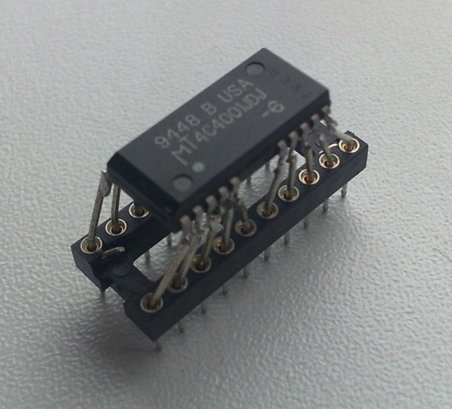
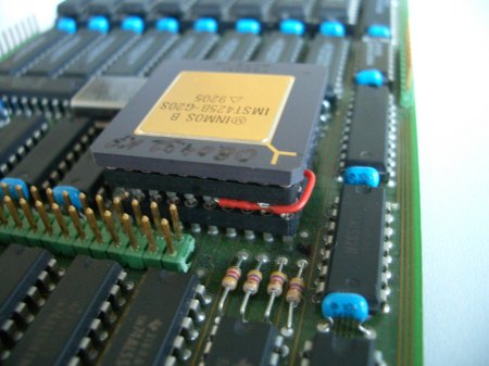
desperRAM3

Here you have it, the ugly Franken-Chip. But hey, it didn’t cost me a dime!
That said, after soldering 160 pins, bending them and carefully pulling them into their sockets… I guess I won’t do it again 😉

The SPEA cards

Between 1990 and 1995 the German multimedia-card manufacturer SPEA was one of the leading companies in this sector (When ATI was comparably small and NVIDIA not even founded).
They offered a wide range of display-cards, from a simple ET4000 up to very expensive CAD/CAM cards using various graphic chips like the TIGA controllers, Hitachi ACRTC, Weitek, S3, 3DLabs and… of course the i860.
Later SPEA was bought by Diamond Multimedia and some employees started their own company to finalize the graphic chip they already started to design when being with SPEA (read more here… article in German, sorry).

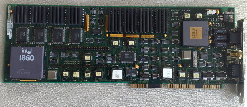
Two SPEA cards using the i860 were built. The first was the

SPEA Fire

SPEA-Fire

This full-size ISA card features a 33MHz i860 with 4MB own RAM as well as 2MB VRAM. An Inmos G364 graphics controller is in charge for creating a picture on the monitor – BTW that’s the last and fastest graphics controller which was manufactured by Inmos.
Theoretically, this card could be called an INMOS B020 on steroids.

As this is “just” a 3D subsystem, a standard VGA was still needed for all 2D stuff. Its video signal was then looped-through the SPEA Fire… just like the Voodoo cards did it some years later.

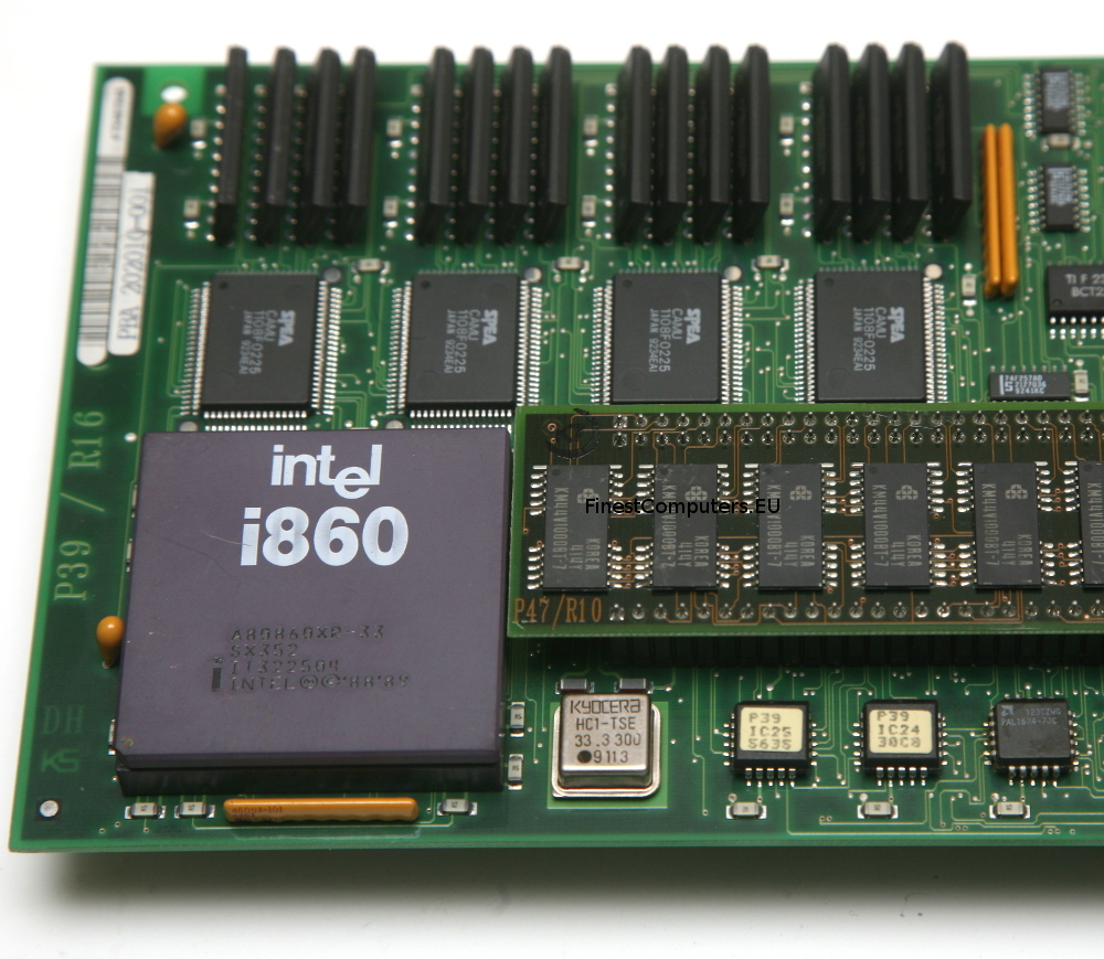
A recent photo I’ve found on ePay shows, that there was a proprietary memory expansion available, which has to be plugged next to the i860. Probably expanding the RAM to 8MB, which can be considered as an quite serious amount of RAM back in those days.

SPEAFire_RAM_upgrade

Interestingly the manual briefly touches the possibility to be programmed with own applications using Intels APX system. Sad enough, the APX is not included on the driver disks and was sold separately for a lot of money.

FGA860

SPEA-FGA860

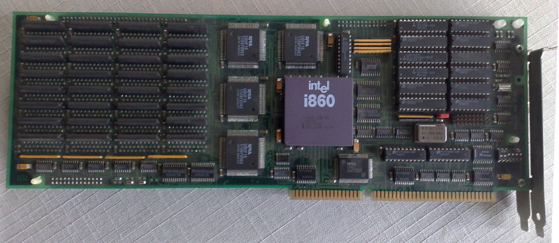
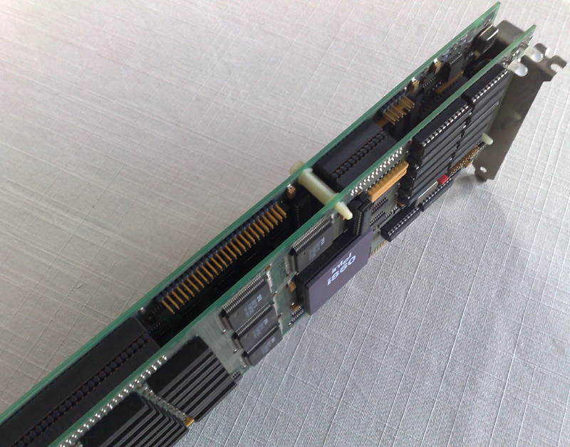
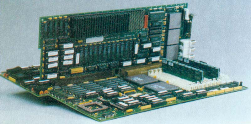
The FGA860 is the bigger brother of the SPEA Fire. Actually it’s two boards sandwiched together: The one on top is -again- called the Fire-Board. But this time it is designed completely different. There is no RAMDAC or such… just the i860, RAM (16MB) and some custom- and bus-logic.
Behind this, there’s a full-blown TIGA card called FGA-4E, using a TMS34020/32Mhz with 4MB DRAM and 2MB VRAM. Not so usual is the also included VGA part on the FGA-4E. This way you can save an ISA slot for the needed VGA card.

The Fire-Board was available for 5700 German Marks, the FGA-4E added another hefty 10.820 Marks making a total of 16.520 Marks (1990/91 that was about US$ 8000)!
But for that money you got a “graphic subsystem” which was capable of 300.000 2-D vectors/s (10 Pixel long) and amazing 30.000 gouraud-shaded polygons/s (10 × 10 Pixels).
[Back then, that really was amazing… today every mobile phone might be better in 3D. Here are some numbers for comparison/amusement:
3DLabs GLINT 300SX: 500.000/300.000]

Here’s a view from the top… not really much to see. It’s very hard to pry those cards from each other. I guess, they were never intended to be separated again.

SPEA-FGA860_sandwich

If you are in need of the drivers, I make them available here. It’s the IMHO most recent version from August 1994 including an AutoCAD 13 driver update.

Hauppauge 4860

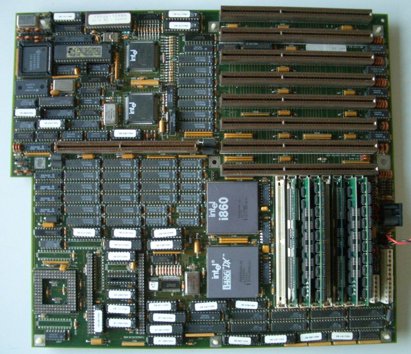
Not really an expansion card but a full blown EISA motherboard featuring an i80486 and an i80860 socket directly on board – thus the ingenious name Hauppauge 4860. The i860 can work in parallel to the i486, both sharing the on-board RAM which can be freely partitioned. But theoretically the i860 could also run completely alone… at least Hauppauge mentions this in the manual, announcing a UNIX version for this option (of course that never shipped).

This board is quite a huge beast, full size AT that is. For its time it was regarded as high-quality but besides 1 ASIC and 2 Intel chip set ICs there are a lot of logic ICs and PALs.
I’d say it’s a ‘IC graveyard’ and one of the most exciting 80486 boards ever made.
(And a real diva when it comes to add cards :-/ More on this further down)

FullBoard

These are the main specs:

  • 80486 socket (does not run stable with DX/2), 25 or 33MHz
  • 80860 socket (same clock speed as 486)
  • Weitek 4167 (aka Abacus) mem-mapped FPU socket
  • Intel “485TurboCache Module” socket
  • 7-8 EISA Slots (depending on revision)
  • Intel EISA chip set consisting of 82358-33 EISA Bus Controller and 82357 Integrated System Peripheral
  • On-board Serial/Parallel and PS/2 mouse support
  • 8 SIMM sockets for up to 64MB (Fast Page Mode,parity – No chance with EDO or non-parity)
  • Award “486 Modular BIOS v4.10” / BIOS level 1.01 -obviously specifically tailored to the 486/860 needs.

Because there are so many things on this manly mainboard, I will go into further detail based on quadrants:

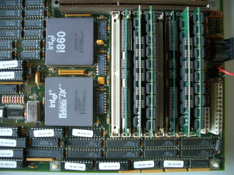
Lower right

LowerRight

Well, that’s where all the mojo sits, right. The two processors side by side – ahhh – what a macho view! 😉 Mind the single oscillator: This means both CPUs run at the same speed, which is a bit of a pity, as the i860 was/is available at clock speeds up to 40MHz. Because Intel never really crossed the 33MHz external clock (the 50MHz 486 was quickly replaced by clock doubling versions due to heat issues) for their 486 processor, this is the highest common denominator.
That said, the Hauppauge 4860 does not support DX/2 processors… believe me I tried them all (even up to 5×86 w/ voltage regulator).Yes, it’s running fine one day while failing to boot the next day. So be sporting about it, an AMD 5×86/133 will easily outperform the i860/33 and who would like to put him ashame like this?

Ok, next to the two brains you can easily spot the 8 SIMM slots. It’s not easy to satisfy the RAM specs here: PS/2 SIMMs, optimally 60ns, Fast Page Mode (FPM) with parity – only up to 8MB per SIMM will be addressed. I had to learn that it is not so easy anymore to find those SIMMs today :-/
At the rightmost edge of the board you can see the classic AT-style power connectors… with an additional connector for 5V. Yup, it’s a server board, having all RAM- & EISA-slots populated, this beast can slurp quite some juice. Ok, it still would be nothing compared to todays insane 1000W power supplies feeding quad-core CPUs and dual graphic-cards.

At the lower edge you can spot quite some logic ICs. That’s a part of the memory interface – yeah, no stinkin’ ASIC, just TTL logic and many GALs.

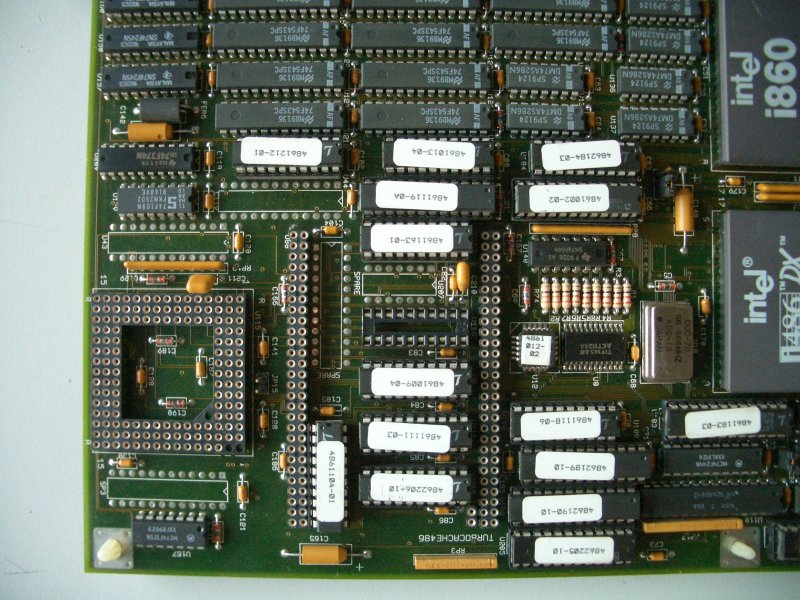
Lower left

LowerLeft

While or two processors still peeking over the right edge, you can easily spot even 2 more sockets on this board. The square one on the left is meant for a Weitek 4167 (also known as  “Abacus”) while the two pin-rows in the middle of the picture are planned for an “Intel 485TurboCache” (yes, that’s 485) module.
Honestly, I have no idea why Hauppauge added the Weitek 4167. As it was just about a bit faster than the inbuilt FPU of the 486/33 (~10% overall), it had no chance against the i860 – both needed programs which were specifically made for them, so compatibility wasn’t an argument for both. I guess it was added on the board just because they could… which is the right spirit!
The socket for the “485 TurboCache” was a good idea – which seems to went wrong in the case of this board. The module generally is nothing more than an i82485 cache controller with 64 or 128k SRAM. After years of searching I found two different models, both not working with the 4860. This seems to be a known issue to Hauppauge as you can find complaints in old (’92) newsgroup posts and Hauppauge itself suggesting not using this module.

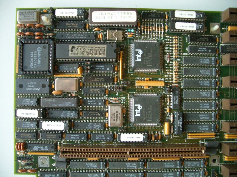
Upper left

UpperLeft

This is the most modern part of the board (as by 1992 standards). It’s actually using ASCIs and not only 80’s-style PLDs. In the top-left corner you’ll spot the Samsung 82C452, which is controlling the 2 serial and 1 parallel port(s) on the board.
Next to it is all the Keyboard/BIOS stuff – one fine thing to mention: Hauppauge used an external battery for the settings/clock. Thanks to god they didn’t use some of those nasty Dallas SRAM/Clock chips. After 10 years the internal battery get weak and there’s no way the replace just that (well, there are ways, but that’s really the last resort).
Now it’s getting serious: ASICs, made by Intel… a chip set! Woohoo! Namely the 82350 Intel chip set (Click here for a lenghty article I wrote about this chip set).
This chip set comprises the 82358-33 EISA Bus Controller (EBC) and the 82357 Integrated System Peripheral (ISP). Together these two devices implement a functional interface to the EISA bus,  and provide most of the standard peripheral functions necessary to implement a minimum EISA solution. In a simple sentence: The EISA interface.
That said, there’s a catch: The 4860 being an early EISA board, does not feature the more ‘modern’ 82358DT EBC you’ll find on most EISA boards. This might be the reason why some EISA cards refrain from working with this board. I found a snippet saying “The 82358DT is a superset of the original 82358 and includes a mode compatible with the 82359 Buffered Bus“. The 82359 DRAM controller is obviously missing (probably not a available at that time) and the RAM controller is implemented in lots’o’GALs.

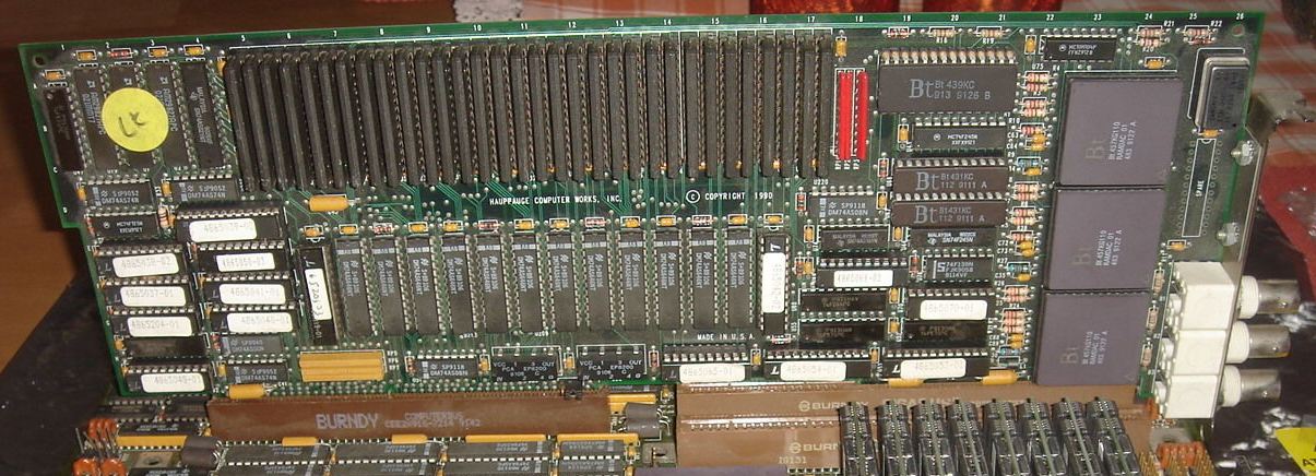
Across the bottom of the picture there’s another slot, looking a bit like EISA… but it’s not! That’s the Hauppauge 64bit Framebuffer Expansion Bus. Hauppauge sold a graphics card basically containing 4MB of VRAM which could be directly accessed by the i860 at very high speed. That made the board a graphics-accelerator like for example the SPEA Fire.

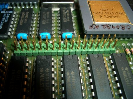
Not much is known about this framebuffer card. Still, I was able to find a blurry press photograph in an 1992 computer magazine. Obviously it’s mainly buffers, GALs, VRAM and 3 RAMDACs for R, G and B… I do have an AutoCAD ADI driver, but I guess you won’t get this board anywhere on the planet anymore 🙁

4860-Framebuffer

Here’s a better photograph I just dragged out of the web:

4860_vidcard

Upper right

UpperRight

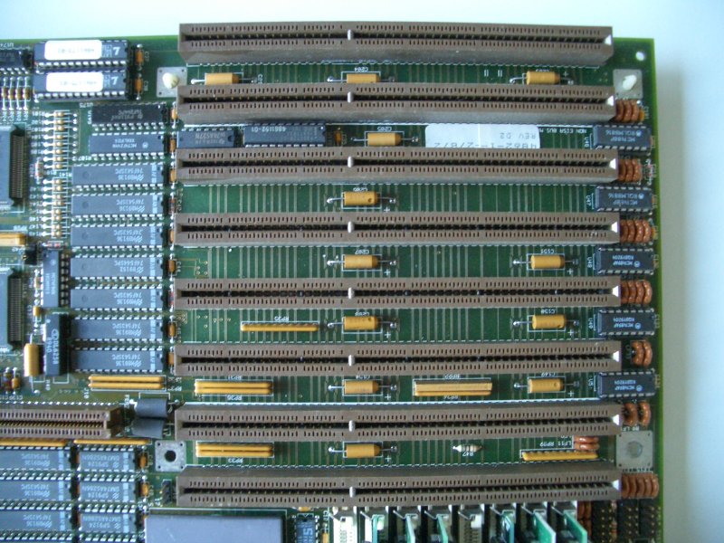
Welcome to the end of our tour… the boring part – at least at the first look. 8 EISA slots and some buffers. Nothing exciting, really.
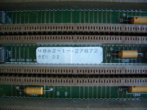
If you take a close look, you’ll see the sticker between slot 6 & 7 (counting from the bottom). This sticker tells you that this board is a “rev D2”:

RevDetail

I don’t have that much documents to figure out the tiny little differences to older versions, but the big one is slot #2. In previous revisions, that slot was ISA… a heritage to this fact is, that on REV D2, this slot is a “non EISA bus master slot” – which is also true for slot #7 (inline with the Frambuffer-Card slot).
The reason for this is (my assumption, though) that the 82357 (ISP) integrates seven 32-bit DMA channels, of which 6 routed to the EISA slots and one used for the Framebuffer.

That’s it for now. I will add new findings as I proceed with my fiddlings.
Thanks for joining the tour, don’t forget to buy a T-shirt in the merchandise shop at the exit…

Software

For the whole enchilada, get the 4860 Manual here. That’s real men reading stuff… i860 source code samples included.

This is the official tools and driver disk and here’s a (yet) small archive containing the ADI drivers for the Framebuffer card and the i860 APX specifically tailored to the Hauppauge 4860 (i.e. won’t run on any other i860 system).

Another nice find: The presentation held at Hot Chips Conference 1990. It gives some more insight into the board design and ideas behind it.

Nostalgia

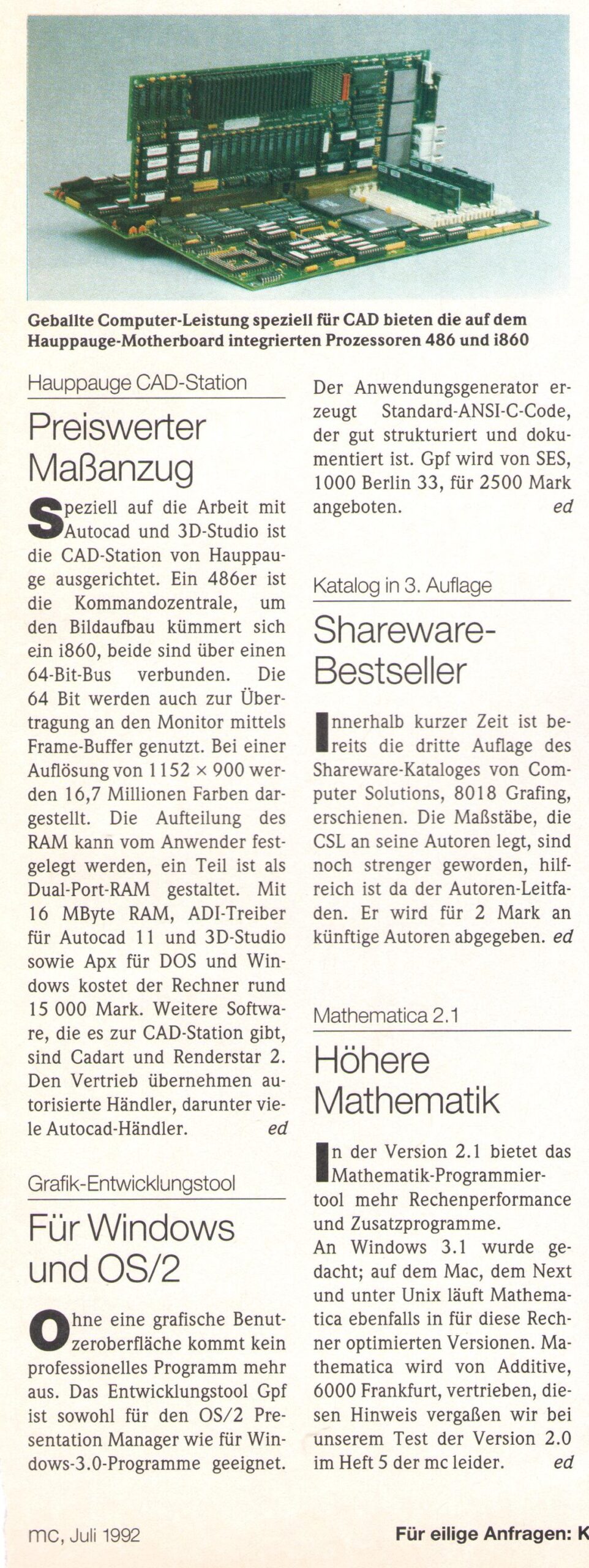
I found a short article in one of my old (German) computer magazines (“MC”, 1992). Here it is for your amusement/riddling:

Microway NumberSmasher

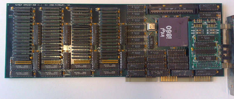
The US company MicroWay (also known for their NDP compiler range), presented an i860 ISA card called NumberSmasher 860.
It was available in two speed grades, costing 11698 DM (@33 MHz) or 14170 DM (@40 MHz). The needed compiler (C, Pascal or Fortran) was an 3135 DM extra.

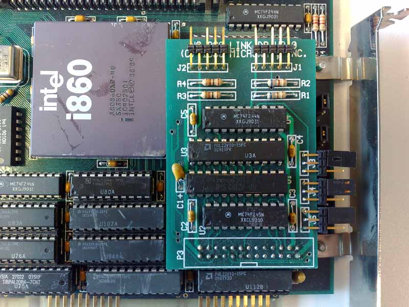
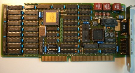
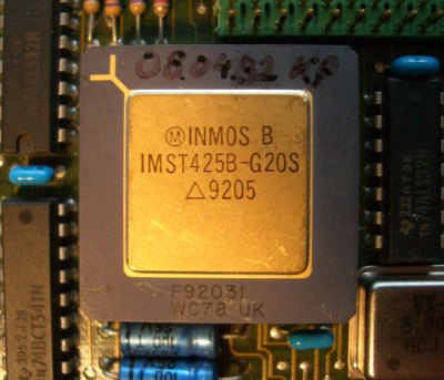
This 16-bit ISA card featured an 40MHz i860, 4 or 8MB of ram and one INMOS OS-link controlled by a IMSC012 on a litte PCB, hiding 2 additional IMSC012 below it on the main PCB.
It is possible to connect one IMS C012 to to the ISA host bus to “feed” the Number Smasher 860 with programs and data (seedocumentation at the bottom of this page).

Here’s the board in its full beauty:

NumSma860

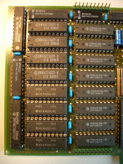
The left half is occupied by the 8MB RAM. The right half is all bus-logic, buffers and drivers. At the top is a very custom HD-connector – thanks to Jörg Heilmann I now know that this is the FiFo-Connector counting 100 pins. Again thanks to Jörg I also have4 pages of documentation to this connector which was designed to connect the FIFO I/O board (available as ISA and EISA version) to.

On a little separate PCB (having “LINK DR V2.0” printed on it) connected to P3 some sort of additional communication part was placed, consisting of an octal transceiver, one INMOS C012 link-adapter a PAL and an octal buffer featuring two 4-pin connectors (J1 & J2).

  • J1 – GND – GND(code) – to pin 3 of J4 – to pin 3 of J3 – GND
  • J2 – GND – GND(code) – to pin 16 of P3 – to pin 14 of P3 – GND

Additionally there are 3 configuration jumpers – function as far as my measurements go:

  • J3 – Connects pin 18 of the board-connector (LinkIn lower onboard C012) to either LinkOut of the C012 (jumper on upper pin) or to the 4th pin of J1 (jumper on lower pin).
  • J4 – Connects pin 20 of the board-connector (LinkOut lower onboard C012) to either LinkIn of the C012 (jumper on upper pin) or to the 3rd pin of J1 (jumper on lower pin).
  • J5 – Linkspeed for the IMSC012  (upper is 20Mbps, lower is 10Mbps)

NumSma860_Link

Documentation

As I have next to no official documentation about this board I would be very glad to hear from anybody who knows the tiniest bit about this card! AFAIK the original “manual” wasn’t bigger than 13 pages… pretty lame for a board costing as much as a small car back in those days.

Thanks to Jörg Heilmann, I got my first piece of original documentation: The 100 pin FIFO-Connector is described on these four pages. Not much but a start!

Here’s what I found out about the P3 connector on the board, having the “LINK DR” PCB plugged into it. If you have a look at the picture above, I’m start counting pins from bottom right continuing zig-zag like this:

26 oooo...oooo 2
25 oooo...oooo 1

1 – VCC
2 – CLK 5MHz
3 – Reset of the C012 (Pin 11) goes directly to the i860 reset-pin
4 – GND
5 – D7 from ISA Bus
6 – D6 from ISA Bus
7 – D5 from ISA Bus
8 – D4 from ISA Bus
9 – D3 from ISA Bus
10 – D2 from ISA Bus
11 – D1 from ISA Bus
12 – D0 from ISA Bus
13 – ???
14 – Pin 2 of the upper onboard C012
15 – ???
16 – Pin 1 of the upper onboard C012
17 – ISA Pin B8 (NoWS)
18 – Pin 2 of the lower onboard C012
19 – ???
20 – Pin 1 of the lower onboard C012
21 – MEMW to ISA
22 – MEMR to ISA
23 – ???
24 – ???
25 – VCC
26 – GND

From these findings I conclude that J2 is directly connected to the upper onboard C012 while J1 is either connected to the lower onboard C012 (J3 & 4 set to upper pins) or to the C012 on the LINK DR (J3 & 4 set to lower pins) which has its data-lines connected to the ISA bus.

On the main-card are 3 other jumpers:

  • J1 & J2 – Set the connection speed of the two C012 on the card
  • J3 – Select the ISA IRQ. Top down: IRQ 10, 11, 12, 15.

Everything else I have for now is a single article from the German computer magazine “c’t” (3/91,p.164 by O. Grau and A. Stiller) giving a bit more insight in the way the card works:

“Das Interface zum ISA-Bus des Hostrechners ist auf einer kleinen austauschbaren Platine untergebracht und basiert auf einem FIFO. Durch ihn geht sämtlicher I/O. Ein vergleichsweise aufwendiges Protokoll sorgt für einen recht langsamen Datentransfer, so besteht jeder Transfer aus dem Kennbyte 0 (Schreiben) oder 1 (Lesen), gefolgt von der Zieladresse (vier Bytes) und dem Datum (vier Bytes).”

The interface to the hosts ISA-bus is located on a small changeable board and is based on a FIFO [buffer]. All I/O is going through this. A comparably complex protocol is the reason for the data transfer being a bit slow. Each transfer consists of a ID-byte (0=write, 1=read) followed by the target address (four bytes) and the data (four bytes).

This “protocol” sounds very familiar to me. INMOS had the same, calling it PEEK and POKE… I’m still evaluating this, so stay tuned.

[11/05/10] Great News! I had some time and did some deeper investigation… hardware archaeology at its best 😉 So read on in the next post… it’s dissection time!

Tower of Power

Having the “Gerlach card” running, I was looking for ways to create something Transputers were made for: A farm, grid, network, cluster – call it what you like.

By a lucky incedent I was able to make contact to some people at DESY, which is one of the world’s leading accelerator centres. DESY develops, builds and operates large accelerator facilities, which are used to investigate the structure of matter. It’s comparable to the CERN accelerator in Switzerland.
I’ve learned that they were on schedule to switch-off a part of their accelerator, namely ZEUS (German), as all the planned research-protocols were finished… and I’ve learned that they use(d) several transputers for data aquisition and real-time analytics!
So after 2 years of shmoozing and sending ASCII-art flowers in mails, I was allowed to give their transputers a new home (else they would have been destroyed – oh my!).

I was surprised to see, that there was not the amount of transputers used as I would have expected (hundreds?). So no wonder they were able to replace the transputers by one single Linux box for the last year of the project, running the transputers as hot-standby backup.
But I also got all their spare-parts and everything else… a good start.

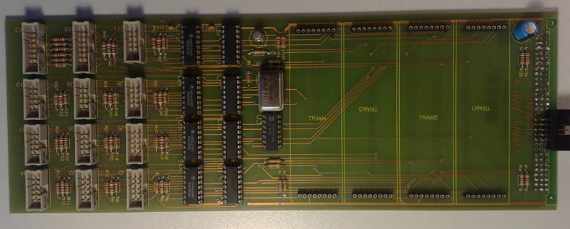
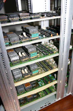
The original system consisted of 12 transputers, each on a TRAM, 4 of those sitting on a custom made TRAM-board called “TRAMWAY” which looks like this:

DESY

It’s not really worth calling it a board – It’s mainly a TRAM carrier with RS422 drivers for each link. The links for the TRAMs are hardwired, so TRAM1 has one “down link” (i.e. from the host or another card) connected to link0. Link1, 2 & 3 are connected to TRAM1, 2 & 3 respectively.

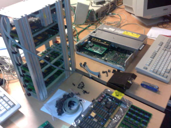
6 of those TRAMWAYs are currently sharing a case making it The Tower Of Power:

TowerOfPower

As you can see I stacked some TRAMs (Size-1 TRAM on a size-2 TRAM) to squeeze in the maximum number of TRAM… power to the tower, man!
Here’s another one showing the ToP with its host, an Intel LP486:

This is how the full power looks like in ‘ispy’:

Using 150 ispy 3.23 | mtest 3.22
# Part rate Link# [  Link0  Link1  Link2  Link3 ] RAM
0 T425b-20 239k 0 [   HOST    …    …    1:0 ] 136K.
1 T805b-25 1.5M 0 [    0:3    2:0    3:0    4:0 ] 4100K;
2 T800d-20 1.8M 0 [    1:1    5:0    6:0    … ] 1028K;
3 T800d-20 1.8M 0 [    1:2    7:0    8:0    … ] 1028K;
4 T800d-20 1.8M 0 [    1:3    9:0    …    … ] 1028K;
5 T800d-20 1.6M 0 [    2:1   10:0   11:0   12:0 ] 1028K;
6 T800d-20 1.6M 0 [    2:2   13:0   14:0   15:0 ] 1028K;
7 T800d-20 1.6M 0 [    3:1   16:0   17:0   18:0 ] 1028K;
8 T425b-20 1.8M 0 [    3:2   19:0   20:0   21:0 ] 132K;
9 T800d-20 1.6M 0 [    4:1   22:0   23:0   24:0 ] 1028K;
10 T805d-20 1.8M 0 [    5:1    …    …    … ] 1028K;
11 T800c-17 1.8M 0 [    5:2    …    …    … ] 2052K;
12 T800c-20 1.8M 0 [    5:3    …    …    … ] 1028K;
13 T800d-20 1.8M 0 [    6:1    …    …    … ] 1028K;
14 T800d-20 1.8M 0 [    6:2    …    …    … ] 132K;
15 T800d-20 1.6M 0 [    6:3    …    …    … ] 132K;
16 T800d-20 1.8M 0 [    7:1    …    …    … ] 1028K;
17 T800c-17 1.7M 0 [    7:2    …    …    … ] 2052K;
18 T800c-20 1.7M 0 [    7:3    …    …    … ] 1028K;
19 T425b-20 1.8M 0 [    8:1    …    …    … ] 132K;
20 T425a-20 1.8M 0 [    8:2    …    …    … ] 132K;
21 T425b-20 1.8M 0 [    8:3    …    …    … ] 132K;
22 T805d-20 1.8M 0 [    9:1    …    …    … ] 1028K;
23 T800d-25 1.8M 0 [    9:2    …    …    … ] 2052K;
24 T800d-20 1.8M 0 [    9:3    …    …    … ] 1028K;

Das Transputerbuch

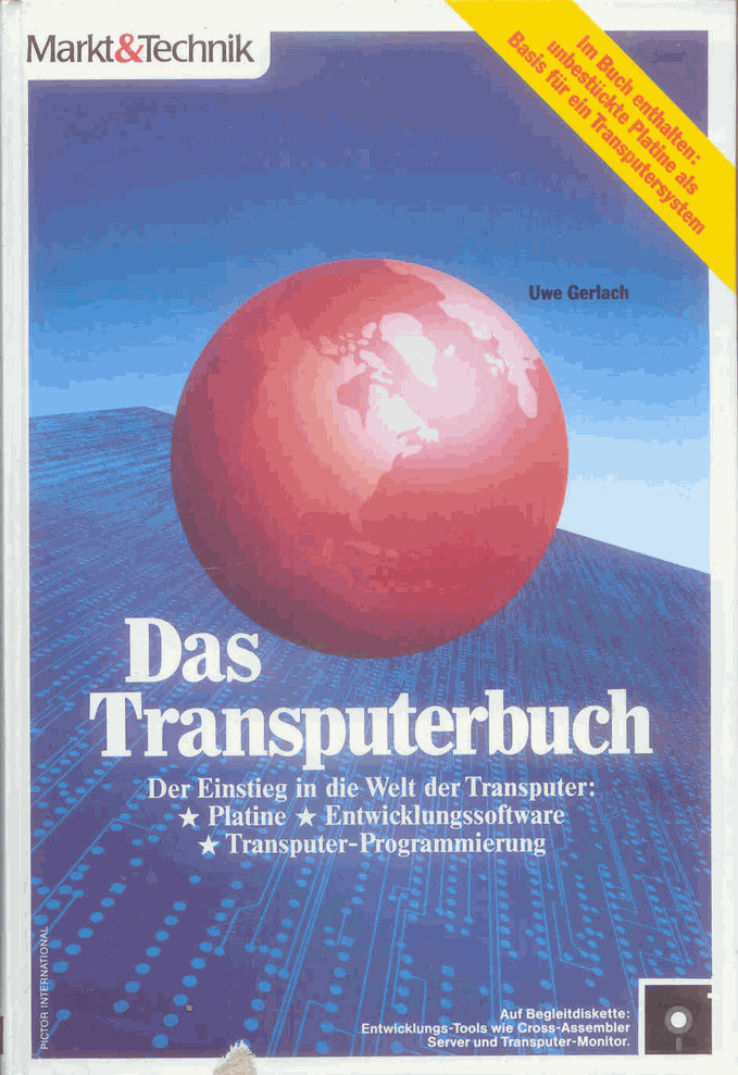
There was one major german book about transputers called “Das Transputerbuch”, written by Uwe Gerlach (ISBN 3-87791-019-X).DasTransputerbuch
What made this book special was that it included an unpopulated 8-bit ISA card for a transputer and 1MB RAM, fully B004 compatible.
Additionally, there were schematics provided to build a host-adapter for several homecomputers of that time (C64, Apple II, ATARI ST and Commodore Amiga).

I was able to get one book off ePay which was still includung the printed circut board and a 360k floppy containing some sample sources and a rudimentary assembler.
So I’ve polpulated it, found some mistakes Gerlach made and made it somehow run.

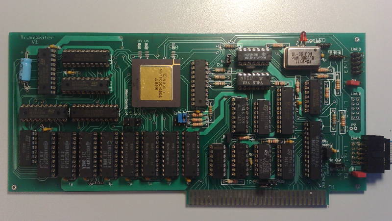
This is how the card looks

Gerlach

It’s design is pretty simple – at least compared to the efforts been taken with the i860 cards on this page. The simple design is also because the Transputer has nearly everything included… so what you see is:

  • The right half is the ISA-bus and link interface. The rightmost and longest IC is a C012 connecting the 8-Bit ISA bus to link0 of the Transputer. Everything else are buffers & drivers.
  • The left half is -besides the Transputer itself- just 1MB RAM and some address-logic. The card would also work without having this side populated using the internal 2 or 4k of the Transputer.

C’est ca. As said, prety simple.

The mentioned bugs of the card are:

  1. The orientation of U11 and U12 are wrong on the print on the PCB and in the book, check the photo for them.
  2. There are no holes for the capacitor near to U28, you will have to solder it to the corresponding pins on the back of the PCB.
  3. The crystal oscillator U12 has its pin-1 not-connected, but it is connected to ground on the board. My crystal oscillator didn’t generate a clock signal, when pin 1 was connected to GND, although it normally shouldn’t matter.

Still, there was a persistent problem with the external 1MB RAM. It was detected by mtest but depending on the Transputer-type used and some randomness, it never was checked as being ok.
Replacing  some capacitors and strengthening some ground traces helped but it’s still not clear what the real reason was.

Here’s the back of the card – looking like a snake-pit now 😉

GerlachBackMod

Motorola M8120

Preliminary, yet lame, M8120 Page

Hi! You just stumbled across our very basic info page about the Motorola M8120 System. Some fine day this will all be redone in 100% Flash…NOT! Anyhow, this is a quick hack but should be sufficient to give you as much info you need about the system.

[For our German readers: Jaja, wie es aussieht, gibt es momentan hauptsächlich deutsche M8120 Besitzer, was man wohl TWC verdanken muß, aber das kann sich ja ändern… sollte jemand Probleme mit Englisch haben, kann er sich gerne an mich wenden.]

What’s a M8120?

The M8120 is a nice little shoebox-sized computer build 1991 by Motorola. The case is just big enough to offer the space for the board, optional memory expansions and the power supply.
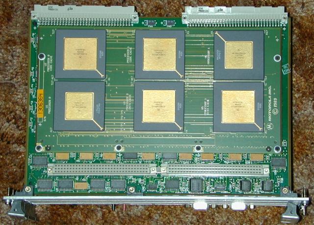
The used CPU is a Motorola 88100, member of the 88k family, clocked at 25MHz. If you take a close look, the mainboard is actually a VME board and a ‘raiser card’ which offers one SCSI, one network and six serial connectors to the outside world.

Hardware

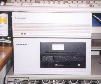
First some pictures…. I know you all love pictures 😉 The system looks like this (pictures generously donated by Michael Schneider):

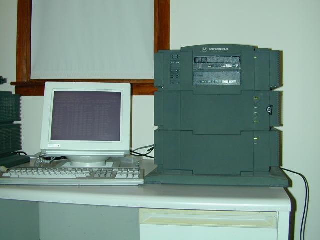
m8120_1

The upper box is the M8120 itself, the lower one is the ‘media box’ containing the SCSI harddisk and a QIC tapedrive.

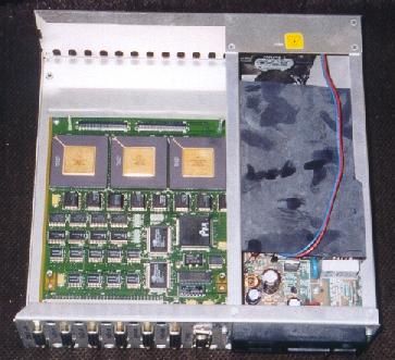
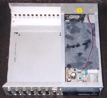
m8120_2  m8120_3

Upper picture: The opened system (Memory mezziane board removed). You’re looking at the mainboard with its 88100 CPU, two 88200 cache controllers (CMMUs) and the Intel network controller.. on the right side it the power supply with its rubber (!) cover.
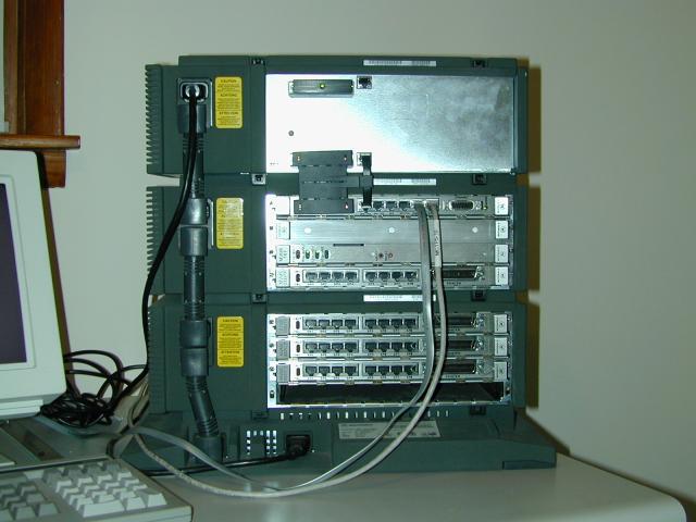
At the back of the system you can see the serial connectors (console, s1, s2, s3, modem1, modem2), the ethernet AUI and the SCSI connector.

Lower picture: And finally this is the bare case with its motherboard removed.

The technical details:

Actually the M8120’s mainboard is a MVME187 board, slightly tweaked to offer 4 more serial ports for the loss of the parallel interface. This moves this little exotic box into the light of standard hardware… well as far as 88k boxes are ‘standard’ these days. So, here’s the list of used components:

  • one 88100 CPU at 25Mhz
  • two 88200 Cache / Memory Management Units (CMMU), 16KB each.
  • NCR53C710 SCSI-2 controller
  • Intel 82596CA LAN controller (10Mbit)
  • CD2401 four channel serial controller
  • 128K static RAM for debugger and diagnostics

The original MVME187 board came in different memory (4-128MB RAM, Parity/ECC RAM) and CPU configurations, having several “sub-models”:

MVME187-001B 25MHZ, 4MB Parity
MVME187-002B 25MHZ, 8MB Parity
MVME187-003B 25MHZ, 16MB Parity
MVME187-004B 25MHZ, 32MB Parity
MVME187-023B 33MHZ, 16MB ECC, 128k L2 Cache
MVME187-024B 33MHZ, 32MB ECC, 128k L2 Cache
MVME187-031B 33MHZ, 4MB ECC
MVME187-032B 33MHZ, 8MB ECC
MVME187-033B 33MHZ, 16MB ECC
MVME187-034B 33MHZ, 32MB ECC
MVME187-035B 33MHZ, 64MB ECC
MVME187-036B 33MHZ, 128MB ECC

As far as we know by the different models being offered on the web, the M8120 seems to be available only with 16, 32 or 64 MB. As we (the maillist members) don’t have a 64MB board, it’s unclear if that is a 33MHz/ECC then.

There’s no RAM on the board itself. It is provided on a mezzanine board on which a 2nd can be stacked.

More details are available in this PDF file from Motorolas library.

Software

The OS installed it System V Rel. 4.0 for m88k. The latest version seems to be R40V4.4… anyone with a more recent version?

No, there’s no Linux for the 88k… if you like to port it yourself, this page (68k MVME) is probably the best start.

New & Exciting! There is a port working of OpenBSD for the MVE187 and the M8120. It runs like a charm on our systems!

Update: The most recent version of OpenBSD/88k is 3.6 (which is true for all supported platforms). While 3.4 and 3.5 boots fine on our litte shoebox, 3.6 gives you some trouble hanging with the message “cl_txintr extra intr” after some boot messages.
Luckily enough, there’s a workaround! Boot into command line mode via

BUG88k> bo 00 00 bsd -c

when you get the prompt enter “disable cl1” and then “quit”. Voilá, 3.6 successfully boots.

Installation HOW-TO: in the works… 🙁 Well, but the official installation manual is quite good!)

Here are two “essentials” I’ve compiled from the original source (not from ports): bash and joe – As I saw quite some downloads for these two binaries, I’ve renamed them to 88k_*.gz just to underline that those are M88k binaries, i.e. won’t work on your x86 Linux box.

Setup

Ok, so you found, bought or auctioned a M8120. Hopefully you got a running system with it. If not, I do have a QIC tape which boots (but still refuses to run on my M8120) I could copy for you if I could boot my machine… you get the point.

What you need for sure is a terminal (or any computer with a RS232 connector) and a cable with at least these tree lines connected:

Signal Pin Pin
TXD (Send) 2 3
RXD (Receive) 3 2
GND (Ground) 7 7

First switch on your terminal being set to 9600bd -8N1, which is the Motorola default. If this doesn’t work (i.e. giving crap on the screen) try different speeds as it could be the case that somebody changed the terminal speed in the ROM (-> See tips and Tricks).
Now start your external media-box and then the M8120.

You should now see the following boot message:

Copyright Motorola Inc. 1988 - 1992, All Rights Reserved

M8120 Debugger/Diagnostics Release Version 1.2 - 04/14/93
COLD Start

Local Memory Found =02000000 (&33554432)

MPU Clock Speed =25Mhz

Autoboot in progress... To abort hit <BREAK>
Booting from: M8120, Controller 0, Drive 0
Loading: Operating System

Volume: $00000000

IPL loaded at: $00FC0000
SVR4 Disk Boot Loader 940112

Probing for devices

.........

Boot: Using EDT built by probe programs
Multiprocessor Kernel Debugger Release 4 Version 6
Copyright (c) 1988 UNISYS.
Copyright (c) 1991-1995 Motorola, Inc.
All rights reserved.
System Diagnostic Command Processor (DIAGPROC Version 94/07/01)
Mentat Portable Streams, Version 3.0
Copyright (C) 1989-1994 Mentat Inc.
All Rights Reserved

Max STREAMS memory = 26043015
Allocating 49K for trace buffers
Found 1 CPU(s)

NOTICE: MP Locking disabled
UNIX(R) MP System V Release 4.0 Motorola m88k Version R40V4.4
Total real memory = 33554432
Available memory = 26669056
Copyright (c) 1984, 1986, 1987, 1988, 1989, 1990 AT&T
Copyright (c) 1991 UNIX System Laboratories, Inc.
Copyright (c) 1987, 1988 Microsoft Corp.
Copyright (c) 1990, 1991, 1992, 1993 Addamax
Copyright (c) 1990, 1991, 1992, 1993, 1994, 1995 Motorola, Inc.
All Rights Reserved

Node: mc88100

Enter <CR> to pause in a single user shell before init.

At this point I was told it switches the line speed to 38400 baud if you’re not hitting CR… but I don’t get this far 🙁

Default boot sequence continuing...
The system is coming up. Please wait.
sadc: Building symbols in /tmp/sa.adrfl for /stand/unix
Configuring loopback interface
Configuring e1x70 interface
add net default: gateway 10.23.1.6 flags 0x3
Starting rpcbind ... done
Starting syslogd
Starting time daemon...done
Print services started.
The system is ready.

mc88100
Console Login:

Tips, Tricks & other findings

Q: What do those LEDs on the cases front mean?

A: The LEDs are different from the MVME187. There are 3 visible LEDs on the front bezel. From left to right those are:

  • RUN – Green : Your system is ON (or off if not lit ;-))
  • STAT – Yellow: System Status, kind of shows the system load. Steady ON means the CPU’s working. It’s software controlled.
  • SCSI – Yellow: If it’s flickering, some bits are running over the bus

There’s a fourth LED on the mainboard not showed to the outside. It’s Red and further right to the SCSI LED (there are two important buttons between them actually, ABORT and RESET). If this LED is on it means FAIL and is not a good sign… 😉


Q: What is the debugger and how do I get there?

A: The debugger could be described as a minimal system to boot your OS, check your system and do some operations similar to todays BIOSes. Hardcore techies will say it’s much more than just a BIOS… and that’s true. But for now, this explanation should be sufficient.
You get into the Debugger by hitting BREAK shortly after the boot process started and you’re asked to hit BREAK to get to the debugger 😉
HINT: ‘he’ will give you a list of available commands.


Q: How can I change my initial terminal speed?

A: Go into the Debugger. Use the ‘PF’ command.


Q: Wow! I like/love/adore the 88k CPU. Are there other machines/boards/systems?

A: Well, quite some. Motorola build several VME boards:

  • MVME187 – The “real” VME version of our little M8120. One 88100, SCSI, serial, parallel and ethernet on-board.
  • MVME188 – Like the 187 but without any onboard peripherals… but with 1, 2 or 4 (!) 88100 CPUs!
  • MVME197 – Like the 187 but using the faster 88110 CPU (LE=one CPU or DP=two CPUs)

These VME boards also came in a stackable case, called the “900 series”. (Front, Back)

Motorola founded a consortium with the aim of creating a multivendor open computing environment based on the Motorola 88000 RISC processor family. This was called 88/open. Some children of this effort been:

The Data General AViiON systems using the 88k family (single and dual, 16-33MHz) running DG/UX. (pictures?)

Finally a Japanese box, the OMRON Luna88k used up to 4 88k CPUs (Back, Inside).

Actually, Jules Richardson revived the original m88k domain. Click here to read more about all the different m88k machines etc.[offline as of 2013]

And then, there is was Paul Weissmann’s badabada.org which is was another cool source for m88k related stuff… you see, you’re not alone! 😉
[Update 2013: Well, it’s getting lonely again… badabada.org went dodo, too
Update 2014: Yay,Houston we have a mirror! badabada.org is back from the grave.
Update 2024: Thanks Götz for hosting a mirror!]

AVM B1 hacking

Intro

Transputers were created to control everything. They were not just CPUs… they could do the video output, control interfaces or even storage devices. So no wonder there were ISDN and SCSI controllers available using transputers.

One of those transputer-sporting controllers was the AVM B1 active ISDN card. Back in the PC-AT days, handling the ISDN protocol and traffic could easily bring down your super-cool 80386/25 without a problem, especially if this machine should also fulfill server tasks.
So active (vs. passive) ISDN cards were the cure to that issue. They featured a CPU of their own with some RAM to buffer the data coming in at the maximum ultra-fast rate of 128kbps 😉

In case of the the AVM B1 the CPU was a transputer (T400) and that had reign over a whopping 1MB of RAM! When the card was installed and the DOS driver booted, it actually loaded the transputer code onto the card like any normal transputer card would be fed with code – behaving like an Inmos B004 card and even using the same port addresses.
So in fact, the AVM B1 is a transputer card featuring an ISDN-part connected to one of the transputers links.

Using the usual tools for finding and checking a B004 compatible card shows this

> ispy | mtest Using 150 ispy 3.21 | mtest 3.21
# Part rate Link# [ Link0 Link1 Link2 Link3 ] RAM,cycle
0 T400b-20 43k 0 [ HOST ... ... ... ] 2K,1 1022K,6.

Weapon of choice


Ok, cool – so where do I get this card?

Well, AVM is still very alive-and-kicking but they’re not building these cards (using transputers) anymore… even if they wanted to, Inmos/SGS killed the transputer back in 1993. So eBay is your friend.

Anything to watch out for?

Yes! AVM build(s) 4 major versions of the B1: V1 to V4.
V1.x – Available as ISA and MCA version. The perfect choice! Everything important is socketed, no SMD parts.
V2.x – ISA version only. CPU & RAM is SMD. Ready to play with but not much to mod.
V3.x – ISA & PCI version. Updated version, same features like V2.x
V4.x – PCI version only. No transputer anymore. “StrongT” Controller… might hint towards a StrongARM based thingy.

Again: If you want to do all the hacks described here you have to get a Version 1.x card!

Enhance it! This is the easy part…

Ok, so I assume you fought hard to get a V1.x B1… it should look like this:
(If you acquired an V2.0 card which is smaller and has lots of SMD parts on it, check out Jonathan Schillings page (German), who did all the mods described here with a V2.0 card)

TheBeast

If you have your card in front of you, you might spot some differences. These are the first two and most obvious “mods”:

  • Change the T400 CPU (e.g. to a T425 or even T800)
  • Add more RAM

The T400 is OK to begin playing with this card, but it only offers 2K internal RAM (vs. 4k in the T425/800) as well as it has only 2 links: One connected to the C012 (and this going to the ISA interface) and one is available. I was under the impression, that AVM might use the other link to interface to the ISDN part, but that seems to be memory-mapped.
Changing to a T425 gives you more internal RAM (=speed) and the possibility to use 3 external links to talk to more connected transputers.
A T800 would be the top-of-the-hill, featuring an FPU which will speed up your Mandelbrot tremendously.

So here’s my T425 which replaced the stock T400. At about 8-10 Euros you should be able to get one at ePay…

CPUChanged

Next up, the RAM. Albeit the standard 1MB are plenty enough for nearly all fooling-around you might plan, there’s another Axel-Law to be followed: “If there’s an empty socket, fill it!”.
Also if you’re going serious and think about running the Helios OS on this card, you’ll better have 2MB!
You need to get eight 256Kx4 chips – they’re pretty common. They should be faster than 100ns… you’ll read later why.

RAMAdded

The eagle-eyed reader might spot the different makers of the RAM chips. That’s because I’ve salvaged 2 old ISA-VGA cards (each 512k) for the chips. All are spec’ed at 80ns.

Another run of the transputer find/check-tools now shows this

> ispy | mtest

Using 150 ispy 3.21 | mtest 3.21
# Part rate Link# [ Link0 Link1 Link2 Link3 ] RAM,cycle
0 T425b-20 43k 0 [ HOST ... ... ... ] 4K,1 2044K,6.

Not bad, huh? But there’s room for improvement… the RAM is accessed extremely slow, set to 6 clock cycles which is very conservative, even for 100ns RAM parts.

Faster RAM – The not-so-easy part…

Ok, up to here it was a piece of cake, wasn’t it? Now we’re switching to hard-core mode 😉

RAM-Access speed-up

For this you’ll need

  • Some soldering know-how – and a solder-iron of course
  • A calm hand
  • A continuity-tester or multimeter
  • A thin cutter
  • the pinout of a transputer (available in the data sheet (PDF))

As said before, the RAM access is very slow. It’s set to 6 clock cycles which is recommended for 150ns parts even at 20MHz. So for a start we should be safe going down to 5 cycles even with the standard 100ns RAM chips…
The RAM is controlled by the transputer itself – something the Intel-World introduced with the AMD Opteron years later!

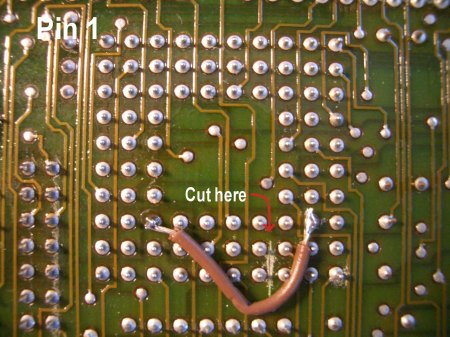
When booting, the transputer checks how his “MemConfig” pin (position C8) is connected to the MemAD[3-7] pins to determine the RAM speed. The AVM B1 has its “MemConfig” connected to MemAD7 (position K10) which we want to change to MemAD6 (J8) in the first step.
The AVM B1 is a 4-Layer card and unfortunately the wire connecting those two pins is running in the 2nd layer from the back.

To find the trace we have to cut, hold the card in front of you looking at the component-side – like the first picture on this page. Now flip it vertically. You’re looking at the solder-side, the external connectors pointing to the left.
A closer look at the transputer pins shows you where to cut and the wire connecting “MemConfig” with “MemAD6” – Pin A1 is in the upper left corner, counting down[123456789,10], letters right [ABCDEFGHJK]!

RamSpeedMod

The cutting is a delicate thing to do. So be very careful not to cut too deep. I did it by cutting carefully once or twice and then checking with a continuity-tester if MemConfig and MemAD7 are still connected. Repeat until the connection is broken.
If everything went fine solder a wire between the two pins. Don’t make the wire too short, so we can change/move it anytime later. Another test shows this now:

Using 150 ispy 3.23 | mtest 3.22
# Part rate Link# [ Link0 Link1 Link2 Link3 ] RAM,cycle
0 T425b-20 43k 0 [ HOST ... ... ... ] 4K,1 2044K,5.

Yay! RAM’s accessed a bit faster now.

If that works and you’re like me (squeezing out the last drip of everything) you can try connecting to MemAD5 (J9). It worked for me.

Faster Link Speed – Not for the fearsome!

The next thing being rather sub-optimal is the link-speed… 43k/s is dran slow.

Using 150 ispy 3.23 | mtest 3.22
# Part rate Link# [ Link0 Link1 Link2 Link3 ] RAM,cycle
0 T425b-20 43k 0 [ HOST ... ... ... ] 4K,1 2044K,5.

That’s because it’s locked to 10Mbit/s by AVMs design even 20Mbit/s would be possible. Again, the transputer gets its configuration during boot-time via special pins. In this case LinkSpecial(A2), Link0Special(B4) and Link123Special(A4).

Not a big deal, but in case of the AVM B1 it’s not solvable by simply putting those pins high or low. That damn card is -again- a multilayer card and one of those layers is a ground-layer. No way in cutting a trace here.
The only solution is an in-between socket… a calm hand and pincers >:-)

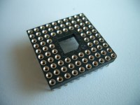
socket_topOk, first you have to get another 84-pin socket. It’s not so easy anymore to find those… luckly, I had one spare collecting dust.

You might find an alternative socket meant for a Motorola 68881/2 FPU – but make sure it also has the inner pin-rows connected. Normally the 68881/2 has 8 pins less!
Another possibillity would be making a socket by glueing 10×1 pin-rows together. Not pretty but should do the job.

For the second step, you’ll need a caliper and (again) the transputer pinout. Orientate the socket so that pin-1 is in the upper left corner (the picture above shows this by the angled-corner in the center of the socket).
Now identify the pins LinkSpecial(A2), Link123Special(A4) and Link0Special(B4) as well as one VCC-Pin of your choice (I went for C2). We need to connect those 4 pins, pulling all Link[n]Specials high… which gives us 20Mbit/s link speed!

Note: If you plan to use the B1’s external links, you might consider not to change the external link-speed – read more about this in the next chapter.
In this case do not change Link123Special(A4).

So carefully cut the thin part of the pins A2, A4 (see note above!) and B4. Use a rasp/file to shorten the pin down to the thicker base (so the remaining part can’t connect to the original socket).
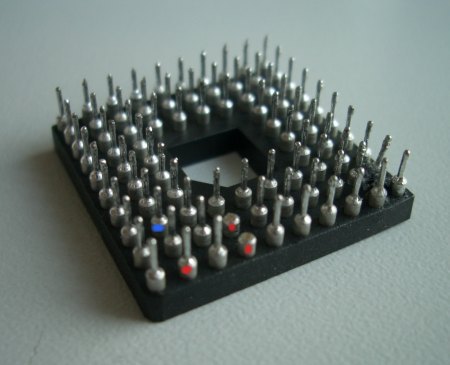
This is how it looks already having A4 & B4 cut off, A2’s still due (all marked red) – Do not cut the VCC-pin (C2, marked blue)! :

socket_pins_cut

When everything’s nicely cut, use a wire to connect them together – it’s a bit tricky to solder between the pins, so use a fine tip.
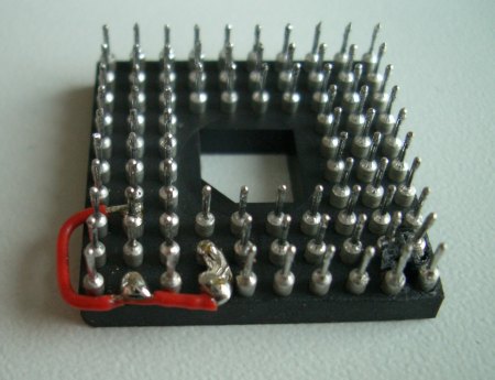
When you’re done, the socket should look like this:

socket_pins_solder

Now double check the modded pins for shorts to their neighbours!! Not doing so might kill your transputer/card!!

Cool! Were half done. For the third step we need to adjust the other side of the link accordingly. “The other side” is the Inmos C012 link-adaptor sitting in the lower right corner of the card -close to the ISA connector- labeled “IMSC012-P20S”.
Identify pin-15 and use a thin caliper to cut its leg as close to the board as space allows it. Bend the remaining leg up and check that there’s no connection to the card anymore.
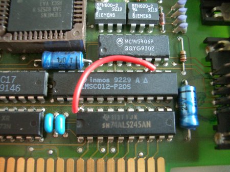
Now solder a wire going from pin-15 to some VCC source. I’ve chosen Pin-20 of the 74ALS245 next to the C012. This is how it looks on my card:

C012_mod

[Note: Make your wire long enough so you can reach some GND pin with it. So you can reverse the mod easily.]

We’re nearly there! For the forth and last step, plug your transputer into your in-between socket and the whole thing into the original socket on the card like this:

socket_seatedt

Done! If everything was done right the usual tools should give you some serious number (well, it’s still far away from the theoretical 1.7Mbit/s, but at least 8.8 times faster than before):

Using 150 ispy 3.23 | mtest 3.22
# Part rate Link# [ Link0 Link1 Link2 Link3 ] RAM,cycle
0 T425b-20 378k 0 [ HOST ... ... ... ] 4K,1 2044K,5.

378k/s is faster than my crappy Gerlach-card (@239k), even the AVM is also just using 8 data-lines of the ISA bus (being a 16-bit card it only uses 4 lines from the AT bus… for IRQs 10-13).

So… what else can be done?

The external Connector

The AVM B1 v1.x cards feature a mysterious (green) connector:

ExpansionPins

It’s undocumented… up to now 😉 I just started tracing all the connections, but I’m happy to say that even AVM did everything possible to cripple the B1 card, they did not dumb it down completely:

Link[123] & Reset (not inverted!) are brought to the outside!! Error and Analyse are hold to GND, though.

Note: That said, AVM wouldn’t been AVM if they didn’t save a dime… the external links are buffered (at least) by a comparably slow 74BCT541 octal buffer.
This offers a signal propagation delay of ~9ns while INMOS recommended to use “F” type buffers, which offer a speed of about 3-4ns. So 20mbps are too fast for this chip. 10mbps should work though.

Here are my findings so far: [work in progress]

I started counting pins from the transputer, zig-zag, downwards. Interesting things coloured green.

1 2
o o
reset o o
o o
o o
o o
o o
PEB2070
o o (to its pin 10)
Link3Out o o
Link2Out o o
Link1Out o o
Link3In o o
Link2In o o
Link1In o o
GND o o
o o
GND o o
o o
33  34

Multiprocessing

Wow! Hier hatte ich wohl richtig Zeit. Multiprocessing in allen Formen und Farben… Mit eigenen Benchmarks und sogar Bildern, die man dazu downloaden konnte, jetzt natürlich in schickem HTML – und es war das letze Posting in der CPU Gruppe, da sich die Mailbox aus dem Netzwerk-Verband verabschiedete .
Mein Meisterstück!

Hallo treue Leserschaft…

Ich möchte mich diesmal über ein höchst interessantes und aktuelles Thema auslassen: MULTIPROCESSING.

Schon des Öfteren gewünscht und durch Windoof NT (im Folgenden nur noch NT) sogar in greifbarer Nähe für den Endanwender ist Multiprocessing (MP) eine recht umfangreiche Sache…dies ist also meine Saisonarbeit. ( Neu ist, daß ich eine Bilddatei im gängigen .BMP-Format beilege, sodaß man sich die beschriebenen Systeme besser veranschaulichen kann. Wenn ich also eine Bildangabe mache…da nachschauen.)

Anm.: HTML kann das natürlich alles besser 😉
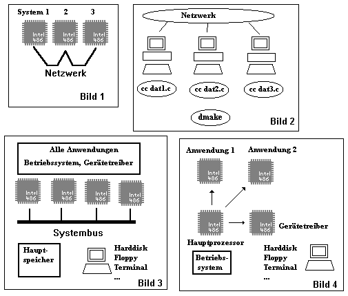
bilder

Nach der grauen Theorie gehe ich im speziellen auf die WYSE MP Rechner ein, denn diese sind nicht nur INTEL (486) basierend (was die Sache irgendwie Greifbarer macht), lange auf dem Markt (und daher Referenzmaschinen bei Microsoft was NT auf INTEL MPs betrifft) sondern wie es der Zufall so will tummelt sich gerade eines dieser pussierlichen Tierchen unter meinem Schreibtisch.
Auch dringe ich etwas in die OS-Theorie, indem ich NT auf den Seziertisch lege und in seinen Eingeweiden herumbohre (Leide, Du Biest!). Auch unter UNIX mußte der Wyse Rechner schwitzen, allerdings nur für Drhystone und Multiusertest. Alles in allem würde ich sagen seid Ihr danach fit für die MP-Welt..wenn dann der erste VOBIS MP Rechner zu kaufen ist 🙂 (Natürlich sollte es kein INTEL Rechner sein, und auch Windows-NT muß es ja nicht unbedingt sein).

Multiprocessing entstand, als man erkennen musste, daß man das Mhz-Rad nicht unendlich drehen, die Architektur nicht endlos optimieren und generell nicht Zaubern konnte. Die naheliegendste Problemlösung war also einfach mehrere Prozessoren an einer Aufgabe knobeln zu lassen. Der einfachste Schritt ist das Verkabeln von CPUs untereinander; wenn man mehrere PCs unter z.B. Windows for Workgoups (WfW) verbindet, hat man, grob gesehen schon ein MP-System. Die Menge an Daten, die über das Netzwerk übertragen werden kann ist natürlich mehr als dürftig, sodaß die Leistung dieses MP-Systems ruhigen Gewissens als erbärmlich bezeichnet werden kann. Man spricht hier von einem MP-System mit “räumlich verteilten Prozessoren” oder “lose gekoppelte Prozessoren” (Bild 1). Typisch ist hier, daß auf jedem Prozessor ein eigener autonomer Betriebssystemkern läuft, der sich mit anderen vernetzten OS abstimmt. Oft fasst man diese Betreibsystemkerne als Verteiltes Betriebsystem zusammen, sog. spreaded- oder distributed OS. Trotz dsr relativ schlechten Durchsatzes eines Ethernet kann ein lose gekoppeltes MP-System eine Leistungssteigerung bedeuten. Wenn z.B. mehrere vernetzte PC nur vor sich hindümpeln, auf Mausbewegungen warten und Toaster fliegen lassen, kann es sinnvoll sein, wenn ein Server gewisse Arbeiten auslagert (sortieren o.Ä) um seiner Aufgabe schneller nachzukommen. Das muß natürlich softwaremäßig unterstützt werden. Eine wirklich interessante Nutzung ist das DMAKE im OS/2 LAN SDK. Es verteilt, von NMAKE gesteuert, die compeillierung über die Rechner im Netzwerk und beschleunigt die Erstellung eines Programmes dramatisch. NT soll das in Zukunft auch ermöglichen (soll!). (BILD 2) Im Folgetext wird MP aber immer gleichbedeutend sein mit: Alle Prozessoren in einem Gehäuse, also “echtes MP”. Weiter werden alle Prozessoren von EINEM Betriebsystem gesteuert. Trotz dieser Reduzierung gibt es immer noch Unterschiede.

* GRUNDLEGENDES

ASMP —- ASMP steht für “Assymetric Multiprocessing”. Hierbei erhält jeder Prozessor eine Aufgabe, für die er optimiert wurde. Üblicherweise führen dabei ein oder mehrere Prozessoren den Code von Anwendungen aus und ein übergeordneter Prozessor den Code des Betriebsyystems. Weitere Prozessoren können bestimmte Peripherieaufgaben übernehmen, z.B. I/O oder Plattenzugriff. (BILD 3) Typisch für ASMP-Systeme ist, daß jeder Prozessor auf seine Aufgabe hin optimiert ist, und es zwischen den Prozessoren klare Hierachieen gibt. Damit man das ganze dann auch wirklich als MP-System bezeichnen kann, muß der Ober- Prozessor den Untergeordneten auch echten Code zuweisen können. Es ist also mehr als übertrieben meinen PC mit i486, ET4000 und i8085 (auf meinem Adaptec) als MP-System zu bezeichnen, da es sich um Peripherieprozessoren handelt, deren Aufgaben hardwaremäßig festgelegt ist und die von OS keine Programme im klassischen Sinne zugeteilt bekommen.

( Beispiele, die mir hier einfallen sind die Groß- und Minirechner um 1985 und explizit die SONY NeWS 1750 (oder so). Hier werkelt ein MIPS R3000 (Main CPU) und ein Motorola 68030 (I/O CPU) nebeneinander.)

SMP

SMP ist dann logischerweise das Kürzel für “Symmetric Multiprocessing”. Es ist das Gegenteil von ASMP und auffälligstes Merkmal ist, daß alle Prozessoren vom gleichen Typ sind und alle auf die gleichen Ressourcen, d.h. Speicher, I/O und Systembus, zugreifen (BILD 4). Da jeder Prozessor freie “Sicht” auf den Speicher hat, kann er jederzeit Code ausführen oder auf I/O Bereiche zugreifen. Der volle Einblick ins System erlaubt auch die Ausführung von Kernoperationen oder von Gerätetreibern. Bei der Begriffswahl zeigen sich einige Firmen von ihrer kreativsten Seite und reden von TSMP (True SMP) und wollen SMP damit wohl als Lügner bezeichen…letztendlich meinen sie aber das Selbe. ( Da fällt mir ein Zitat von Kohl ein:”Letztendlich steht es jedem Bürger frei, ob er seinen Dienst an der Waffe verrichtet, oder seinen Friedensdienst bei der Bundeswehr ableistet…”, naja, zurück zum Thema )

Es stellt sich die Frage, was bringt mehr? Es hat sich gezeigt, daß SMP mehr leistet, da der Verwaltungsaufwand für das OS geringer ist als bei ASMP. Die Kerne die auf den einzellnen Prozessoren wägen selbst ab, welche Aufgabe sie übernehmen. Stellen wir uns drei Prozessoren vor, A, B und C. A wartet auf ein I/O Gerät, dessen Ergebnisse er zum Fortsetzen seiner Arbeit benötigt. B bearbeitet eine Hintergrundarbeit niedriger Priorität. C arbeitet voll ausgelastet an einer Datenübertragung. Jetzt kommt der dumme User auf die Idee die Maus zu bewegen. Hektik und Chaos bricht über die drei Jungs herein. Der Prozessor mit der “unwichtigsten” Arbeit (B) nimmt sich also der neuen Aufgabe an (der Meister ist schließlich am anderen Ende der Maus!), und stellt die alte Aufgabe hinten in ein Aufgaben-Pool an. Während C immer noch eifrig Daten packt und überträgt hat sich bei A mittlerweile das I/O Gerät gemeldet und er konnte seine Arbeit beenden. C nimmt nun die Aufgabe aus dem Pool und setzt diese fort. B kämpft währenddessen immer noch mit der Maus (User?). Die Vorteile zeigen sich schnell: Prozessoren können Aufgaben beliebig tauschen, oftmals sogar ohne Softwareunterstützung, und wenn mal eine CPU ausfallen sollte…who cares, übernimmt eben eine Andere, lediglich die Leistung des Systems wird gebremst. Umgekehrt, legt man ein paar Brikets (in Form von CPUs) nach, wird das gesamte System schneller. NT unterstützt somit standardmäßig SMP, wobei Hersteller von ASMP-Hardware NT mittels spezieller Treiber auch zu einer Arbeit unter deren System bewegen können. Hierauf will ich aber nicht eingehen, da ich dies in meiner unendlichen Weisheit als unwichtig erachte 🙂

In medias res (oder: zur Sache, Schätzchen)
——————————————-

Wie Eingangs angedroht kommen wir jetzt zur Praxis. Der dunkelbraune Klotz, der die Luft unter meinem Schreibtisch heftigst erhitzt, hört auf den Namen Wyse Serie 7000i Model 740 oder besser 7000i 740MP-3/32E/4M. In ihm schwitzen 3 i486/33 auf ihren jeweils privaten EISA Karten und werden von 32MB Speicher und 425MB Fesplatte umspült. Die Prozessoren kommunizieren über einen 64Bit breiten, bei 80Mhz getakteten Bus. Da alle Komponenten zusammen ordentlich einheizen, befindet sich sowohl ein Lüfter im 325 Watt Netzteil als auch einer direkt vor den drei CPU Karten. Die beiden machen einen Lärm wie eine alte VAX, was auch der Grund dafür ist, daß ich diesen Text auf meinem 0815-PC schreibe :-). Generell wäre das auch auf der 740 möglich (Ja, große Rechner sind WEIBLICH), da sich ein Phönix BIOS auf dem Motherboard findet. Jedoch ist ein MP dann nicht möglich. NT erkennt beim Hochfahren die anzahl der Prozessoren und kann diese dank HALWYSE7.DLL auch richtig initialisieren. Das ist kein Wunder, denn die 740 ist das offizielle NT for Intel MP-Referenzgerät. Wyse hat schon neue Geräte angekündigt oder vorgestellt. Das Modell 760 bietet 3 i486/DX2 und ist somit annähernd doppelt so schnell. Die angekündigte 790 soll wahlweise 3-4 DX/2 oder Pentium beherbergen, aber wie dem auch sei, alle basieren auf dem gleich Layout (und beschissenem Prozessor, wenn ich mir die Bemerkung erlauben darf). Es ist mir allerdings ein Rätsel warum Wyse diese Prozessoren gewählt hat. Klar, man kauft mit Intel ein riesen Stück Kompatibilität. Auch ist man einer der ersten Hardwareanbieter für NT-MP Systeme. Aber der i486 ist kein MP-Prozessor, muß also durch viel Hardware-drumherum dazu gezwungen werden…und er ist nicht mehr der Schnellste, woran auch Pentium nichts ändert (die lahme Krücke :-)). Schnell ist dann der Erste der Letzte, wenn andere einen Alpha oder einen MIPS 4400SC einsetzen und die eigene Architektur nur 32 Bit Intel-Krüppel unterstützt. Wow, der Dampf musste mal abgelassen werden. Jetzt aber nüchtern weiter, vielleicht ließt mein Sponsor ja auch in diesem Brett und dann müßte ich mich aber ganz schön auf dem Boden rollen um nochmal Gnade zu erhalten. Man bekommt ja nicht alle Tage eine 55.000.- Kiste geliehen 🙂

Wie schon erwähnt greifen alle Prozessoren auf gemeinsame Ressourcen zu. Dazu ist es natürlich erforderlich, daß ein einzelner Prozessor die anderen per Interrupt Signale zuwinkt, um z.B. eine Änderung des gemeinsamen Systemspeichers bekanntzugeben. Das Lesen und Schreiben von Speicherbereichen ist als sequentielle Operation realisiert. Speicherzugriffe werden in der Reihenfolge abgearbeitet, in der einzelne Prozessoren Daten vom Bus fordern (first-come-first-serve). Ein “Multi-Stage-Pipelining” ermöglicht das Überlappen einzelner Zugriffe, sodaß das System den nächsten Datentransfer zwischen CPU und Speicher schon vorbereiten kann, bevor der erste abgearbeitet ist. Wie wohl jeder schon mitbekommen hat, besitzt der i486 einen internen Cache, der den Zugriff auf den Systemspeicher begrenzen und damit beschleunigen soll. Falls mehrere Prozessoren identische Speicherbereiche in den Cache geladen haben, muß spezielle Hardware dafür sorgen, daß alle Prozessoren mit denselben Daten arbeiten. Dazu hat Wyse ein Kohärenzmodell realisiert, das der Software ein kohärentes Bild des Systemspeichers bietet. Im Cache befindliche Daten befinden sich in einem der vier Zustände “Modified”, “Exclusive”, “Shared” oder “Invalid”. Daher kommt der Name des gängigsten Kohärenzmodells “MESI”, das die meisten MP Systeme nutzen (Dazu weiter unten mehr). Um den Zustand der im Cache befindlichen Daten nicht zu “vergessen”, hält die Logik diesen im sog. Cache-State-TAG-RAM bereit. Ohne diese Logik ist das Chaos leicht denkbar: Ein programm lädt einen Speicherbereich kleiner 8K in den Cache und im laufe der Abarbeitung des Codes wird auch nur dieser Bereich geändert. Wenn es fertig ist schreibt die Cachelogik nun alles zurück in den eigentlichen Hauptspeicher. Währenddessen tun dies aber auch 1-7 andere Prozessoren. Der Hauptspeicher wird inkohärent oder besser gesagt: Ist nicht up-to-date. Manche Prozessoren arbeiten mit “alten” Daten, da sie nur auf den Cache (inten und extern = 264K) achten, nicht aber auf vielleicht durch andere Prozessoren schon geänderte Inhalte im Hauptspeicher. Die Folge: Totale Verwirrung, was gemeinhin zum Absturz führt.

M.E.S.I.
——–

MESI ist ein, wie oben beschriebenes Datenkohärenzprotokoll für MP-Systeme mit Cache. Grob umschrieben sorgt es für einen Abgleich der Daten im Cache und im Hauptspeicher. Hier kurz die Zustände:

(wenn es möglich wäre, wäre das hier jetzt ein grauer Kasten, naja, dann halt so, ne, GRAUER-KASTEN-AN 🙂

– M odified Die Cacheline befindet sich exclusiv im Cache, sie wurde aber neu beschrieben (dirty) und ist nicht up to date im Hauptspeicher. Lesen und Schreibe ist ohne Zugriff auf den Bus möglich.

– E xclusive Die Cacheline befindet sich unverändert im Cache und im Hauptspeicher. Lesen un Schreiben (dann Wechsel nach “M”) ist ohne Buszugriff möglich.

– S hared Die Cacheline befindet sich auch in einem anderen Cache, und sie ist immer aktuell. Lesen ohne Buszugriff möglich, Schreiben ist immer ein write hit (ich würde es lieber Write Update nennen) und führt zum Update des Hauptspeichers. Das Invalid Signal wird aktiv, und alle sharing-Partner haben die entsprechende Zeile zu invalidieren. Damit entfällt Zustand “S” und wechselt auf “E”

– I nvalid Die Cacheline ist ungültig oder nicht im TAG-RAM vorhanden. Sowohl Lesen (Read Miss) also auch Schreiben (Write Miss) bedürfen eines Buszugriffes. Über die WT-Leitung (Write-Trough) erfährt der Cache, ob er mit Kollegen das Datum sharen, also nach “S” oder sonst nach “E” gehen soll.

(GRAUER-KASTEN-AUS)

Das MESI Protokoll ist bei den meisten modernen CPUs intern schon vorgesehen, d.h. ein MP System auf Basis dieser CPUs benötigt keine zusätzliche Hardware wie es bei der 740 der Fall ist. Prozessoren dieser Art sind z.B. Der MPC601, MIPS 4400MC, SPARC10 aber auch der Pentium. Dieser & MIPS bietet nebenbei auch ein interessantes Feature namens Master-Checker-System. Hierbei bearbeiten zwei CPUs exakt den selben Code ab und vergleichen ständig ihre Ergebnisse. Wenn die Ergebnisse nicht übereinstimmen wird das noch zweimal wiederholt und dann an einem Pin gemeldet. Die umgebende Rechnerlogik sollte dann schleunigst etwas mit dieser Meldung anstellen, z.B. Den Supervisor benachrichtigen, den aktuellen Zustand sichern, allen Angestellten frei geben, ein Bier trinken oder was weiß ich. Das ist aber kein MP!

Maximale Theorie
—————-

Hier will ich schnell die Ackermann-Funktion erklären, die ich mir vornahm, um ein NT-MP-Bench zu schreiben. Der deutsche Forscher Friedrich W. Ackermann (1896-1962) hat sich besonders mit rekursiver Funktionen beschäftigt. Ich konnte es mir nicht verkneifen den PC-Soderzeichen-“schatz” zu nutzen, alle nicht-PC User bitte ich also um verständnis. Anm.: Durch Grafik ersetzt, HTML wär damals echt toll gewesen 😉 Die Ackermann-Funktion ist ein Integral folgenden Ausmaßes:

ackermann

Die Funktion kann auf einem Computer nur für sehr kleine x-Werte berechnet werden. Die Ergebnisse sind dabei an und für sich nicht besonders aufregend, naja es reicht nicht ganz zur mathematischen Ejakulation 🙂

ack(1,m) = m+ 3 ack(2,m) = 2 * m+ 3 ack(3,m) = 2^(m+3) – 3

Werte für n=4 oder höher können aufgrund von zuwenig Speicher nicht mehr berechnet werden. Das schöne an der Ackermann-Funktion ist, daß man mit ein paar Zeilen C und ziemlich kleinen Zahlen jeden noch so schnellen und speichermächtigen Rechner dicht machen kann (sowas wie ein Joint für den PC). Aufgrund der starken Rekursivität wird nämlich einerseits die Funktion recht häufig aufgerufen und andererseits sehr viel Speicher auf dem Stack benötigt. Im Benchmark selbst wurde die Funktion ack(3,10) benutzt, die sich nicht weniger als 44.698.325 mal selbst aufruft und dabei einen Stack von rund 230K Größe benötigt. Mit jeder Erhöhung des m-Wertes bei n=3 wird die Funktion rund viermal häufiger aufgerufen. Auf meinem 486/33 benötigt eine einzelne Ausführung der Funktion ca. 0,830 µs. Der Benchmark benötigt werder Fließkommaoperationen noch Zugriffe auf die Peripherie und kann auch zur Beurteilung eines Copilers und dessen Parameter- übergabe benutzt werden (toll, was?). Compiler die gut optimieren, erkennen nämlich, daß die angegebenen Parameter innerhalb der Funktion nicht verändert werden und vermeiden unnötige kopieraktionen auf dem Stack.

Jetzt aber SHELL
—————-

Ladies and Gentlemen…NT first

Wozu all die graue Theorie…jetzt wollen wir’s aber wissen! Wie schnell ist die Rübe denn? Wie heiß sie ist wissen wir ja schon (ca. 60 Grad!). Unter NT gibt es ein nettes Tool namens CPU Thermometer, daß dem geneigten User die Auslastung des/der Prozessor(s/en) mit toll-bunten Balken anzeigt. Einmal gestartet sieht man…

Windows NT Multiprocessing benchmark. Copyright (c) 1993 by Axel Muhr Starte den Ackermann(3, 10): Ergebnis: 8189, benötigte Berechnungszeit: 37875 ms.

Ein Balken schlug sofort auf 100%. Gut der ist ausgelastet…der Rest der Bande ruht sich aber aus und wandelt unnütz Strom in Wärme. Also startet ein fieser Axel ein Batch, daß den Benchmark dreimal hintereinander auf NT loslässt (per start /b mpbench.exe). Auf dem Bildschirm kann man folgendes ablesen:

Windows NT Multiprocessing benchmark. Copyright (c) 1993 by Axel Muhr Starte den Ackermann(3, 10): …(Hier das ganze noch 2 mal) Ergebnis: 8189, benötigte Berechnungszeit: 51615 ms. Ergebnis: 8189, benötigte Berechnungszeit: 52060 ms. Ergebnis: 8189, benötigte Berechnungszeit: 54690 ms.

Huch! Langsamer? Obwohl alle drei den gleichen Code verwenden, aus gleichem Stall kommen. Naja der Unterschied ist nicht gerade gravierend. Trotzdem verbrachte ich einige Minuten (zusammengerechnet) auf dem Klo über dieses Phänomen sinnierend. Experimente zeigten, daß z.B. das Schließen des CPU Thermometers den Benchmark beschleunigten, und zwar um ca. 15%. Doch eigentlich erlag ich nur einem logischen Trugschluß, denn:

Ausführung einfach : 37.3s Ausführung dreifach: 39.3s, 43.5s und 44.0s…im Schnitt: 42.23s

Damit ist die parallele Ausführung zwar um 13% langsamer als die Einfache, jedoch hätte die dreimalige Aüsführung NACHEINANDER 112 Sekunden benötigt und damit ca. 2,65 mal länger gedauert. Nach meinen Berechnungen müßte ein 486er hierfür 88Mhz haben, um das mit nur einer CPU zu erledigen. Zudem darf man nicht vergessen, daß bei der MP-Ausfürung auch einige Zeit für Protokoll und NT-Internas “draufgeht”, was die 13% wohl oder übel rechtfertigen könnte. Natürlich zweifle ich auch ein Bißchen an NT, GetTickCount und dessen Genauigkeit, was in einem MP System auch eine recht kitzlige Angelegenheit ist. Sagen wir…MP unter NT ist zugegeben eine nützliche Sache.

…and now, last but not least…UNIX
————————————-

UNIX habe ich eigentlich nur installiert, um Mr.Drhystone in seiner gewohnten Umgebung und einen Multiusertest laufen zu lassen. Eben besagter Drhystone ist nicht gerade das, was ich MP-Freundlich nennen würde. Also C-Compiler angespitzt und ran an den Feind. Tage und Nächte durchgehackt (dramatisch, dramatisch) und nix bei rausgekommen. In meiner Verzweiflung fand ich dann in den Netzuntiefen dieser Welt einen MP-Drhystone, der schon auf MP-SUNs erfolgreich lief. Ruck zuck lief er auch auf der 740. Ergebnis: Gleiches Bild wie unter NT, ungefähr 2,8 – 2,9 mal bessere Leistung gegenüber einem Single CPU System…quod erat expectandum (was zu erwarten war). Zu erwähnen sei noch, daß es unter UNIX viel mehr Spaß macht dem Benchmark zuzuschauen, denn hier gibt es ein Monitorprogramm, das sogar alle Systemcall-Aufrufe und vieles mehr anzeigt. Abgesehen von der Leistungssteigerung sehe ich den Hauptsinn im MP bei Multiusersystemen bzw. -anwendungen. Denn ein Single CPU System geht sehr schnell in die Kniee, wenn es viele User bedienen muß. Deshalb sind fast alle Bankcomputer (incl.Kreditkartenfritzen) MP-Systeme. Keiner will schließlich bis zu 20s warten bis die Auszahlung bestätigt ist (man hat ja schon 10 min in der Schlange hinter den Rentnern gewartet). Der sog. BYTE-Benchmark erzeugt unter UNIX beliebig viele Pseudo-User und man kann den Leistungseinbruch des Systemes dann anhand eines CPU Thermometers (wie unter NT) ablesen. Während ein “Normales” System bei ca. 16-32 Usern extrem in die Knie geht, blibt die 740 bis 512 (!) User standhaft. Ich konnte an der Console sogar noch passabel weiterarbeiten. Bei 1024 Usern verabschiedete die 740 allerdings Sang- und Klanglos in den Tiefen des Siliziumnirvanas. Schade, denn sowas kann bei UNIX Systemen u.U. für den Systemverwalter ewiges Reorg oder schlimmer Reinstall bedeuten. Der Fehler liegt aber meineserachtens nicht an der MP- Hardware sondern an WYSEs UNIX, daß nicht gegen einen zu häufigen fork-Aufruf geschützt ist. 1024 User sind übrigens nicht utopisch, denn unter UNIX ist jeder Task praktisch ein User. Wenn ein Programm z.B. 10 Untertasks (Childs) startet, dieses Programm gleich doppelt pro User läuft und mehrere User an vielen Terminals arbeiten, reichen 50 fleißige Mitarbeiter um das System zu schießen. Und 50 Systemuser (also Menschen) sind in einem Büro-MP-System nicht gerade viel…

Kurz zusammengefasst
——————–

Ein MP-System ist momentan (ganz zu schweigen vom Preis) nicht für den Otto- Normal-User gedacht. So wie die Hersteller es anpreisen funktioniert es zudem auch nicht. Einfaches Nachstöpseln von Prozessoren schließt eine Ver-n-fachung der Leistung nicht ein. Denn für jede CPU zusätzlich hat das System mehr Verwaltungsoverhead. Zudem ist ein unbegrenzter Ausbau auch (noch) nicht realisierbar. Es hat sich gezeigt, daß 8 Prozessoren das Maximum darstellt, um ein MP-System (sinnvoll) zu betreiben. Denn dann ist der Verkehr auf dem CPU- Bus allein Protokollmäßig dermaßen hoch, daß kaum noch Platz für Daten ist.

Busverkehr
———-

Der Flaschenhals ist also wie fast immer der Bus. MP-Buse beginnen bei 64 Bit breite und enden im Highendbereich bei 256-512 Bit. Es versteht sich von selbst, daß hier jeder sein eigenes Süppchen kocht. Sun nennt es M-Bus, Wyse spricht vom WYDE-Bus (Wie originell) und andere nennen das Kind FutureBus. Ein Weg aus dieser Misere, wenigstens für den Pentium, will LSI bieten. LSI legt den MPI-Bus als Standard vor. MPI soll das Low-End für den (zukünftigen) Normaluser stellen. Maximal 4 Pentiums finden auf diesem 32/64 Bit-Bus Platz. Generell ist er genau auf dessen Architektur zugeschnitten, also 64 Bit Daten-, 32 Bit Adressbus, Interne MESI Nutzung, 30 oder 33,3Mhz Bustakt (Maximale Bandbreite bei 33Mhz 267 MByte/s). Alle Bussysteme sollen per Bridge unterstützt werden, wobei PCI der Basisbus ist. LSI will jetzt mit der Auslieferung des Chipsatzes der auf den Namen HT354 (Cache Controller), HT355 (Memory Controller), HT 352 (Bus Controller) und HT353 (PCI to EISA-Bridge Controller) beginnen. Alles in allem eine begrüßenswerte Initiative, denn somit ist nicht mehr alleine der Hersteller des MP-Systemes Anbieter der CPU-Karten. Auch eine Mischbestückung ist denkbar.

Et voila, la fin!
—————–

Das war sie, die fast 450 Zeilige MP-Mail. Ich hoffe Ihr seid jetzt etwas schlauer, was MP angeht und lasst Euch einen ATARI Falcon nicht mehr als MP-System andrehen 🙂 Ich denke das es die letzte große Mail vor Weihnachten ist, und zudem habe ich gerade vernommen, daß die 7*up (meine Box) sich aus dem LightNet verabschiedet (nein, ich kenne die Gründe auch nicht) und ich mir für dieses Brett also eine neue Box suchen muß :-((

mfg AXEL