All posts by Axel

http://www.geekdot.com/about-me/

SuperCluster

The Parsytec SuperCluster was the first system moving away from the classic Eurocard (wikipedia) based machines like the predecessor “MegaFrame” – also, due to the availability of the FPU in the new T800, the previously supporting Motorola M68881 was dropped.

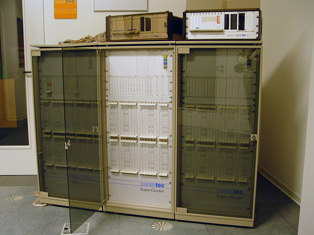
This is how a SuperCluster looks like (NB: Two MegaFrames sitting on top of it):

SuperClusterTotale

(This specific system still stands as an exhibition in the halls of the University Paderborn. It has 320 Transputers, 4MB RAM each, total performance is about 1.1 GFlops/sec. Picture courtesy of “[CD]Overkill”)

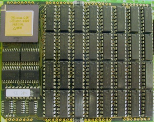
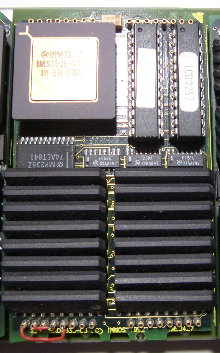
This is the CPU Module (4 nodes, 4MB each) – while being bigger because of the use of many DIP parts, the basic design is very similar to the later GigaCluster node:

MegaFrameTotal

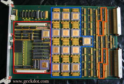
And this is the so-called NCU- or XBAR-Module (Network Connection Unit/Crossbar, in this case the “L” version) consisting of 13 C004 Network-switches and one controlling T425 Transputer:

MegaFrameXbarDetail

A “Map” of the NCU (Red CPU-Node, Blue C004s, Orange RS422 transceiver):

MegaFrameXbarMap

If my interpretation is correct, 4 CPU Modules were combined with one NCU, so 16 Transputers were connected to a 12-C004 Network using the 13th C004 to connect this “Cluster” to the ‘outside’, e.g. backplane with more Clusters.

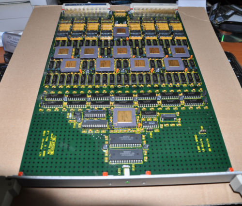
For completeness sake, here’s a picture of the NCU “version R”. It consists of just 10 C004 and the controlling Transputer is a T222 – given its layout in pure DIL, this might be the predecessor of the L-model.
As I’ve learned from another “SuperCluster Enthusiast” (That probably makes it 2 world wide ;-)) both NCUs were used in a SuperCluster. “L” and “R” simply stands for “Link” and “Reset”, so those signals were handled by separate NCUs.

SC_XBAR-R

The two larger ICs in front of the T222 are SRAMs (64K total) making the design even simpler.

x’plorer

It’s yet unclear how to write its name correctly. Some sources use XPlorer, others xPlorer and many other permutations. As my model has this logo at the front of its case xpl_logo

I’m going to use x’plorer. Having this burning issue off my chest, let’s go into details 😉

The x’plorer is more or less a single “slice” -Parsytec called them cluster– of a GigaCube, which used 4 of those clusters in its smallest 64-Transputer version (GC-1). Thus, the  x’plorer features 16 Transputers, each having access to 4MB RAM in a gorgeousdesktop case. If you want, you could call it a “GC-0.25”. xplorer_freigestellt
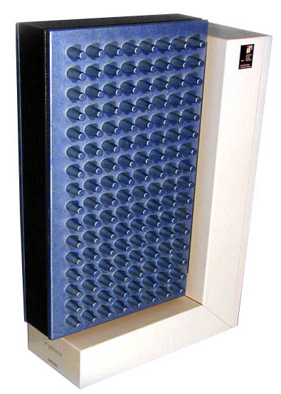
Sorry, but I have to rave a bit over its case design. I first saw it at CeBit fair 1995, when is was on display at the “IF forum design” (I explained that in the Parsytec intro already). I was literally pulled through the room and stood in front of it for minutes.
It looked like a typical FROG design work (Famous for the NeXT cube, Apple //c, some 68k Macs, SPARC Stations and much more) and I told this everybody who asked… but I just figured out I was wrong and it was actually designed by a relatively small studio called Via 4 Design.

The grey L-shaped base/back is made of sheet metal and contains the power supply in the base, a tiny bit of logic (described further down) and 2 big fans in the back.

The big blue main body is made of cast metal – no puny plastic crap. Yes, it’s heavy.
At first sight everybody thinks “hey, that’s a clever design, using the case as a heat sink!”. That’s obvious as those fingers/burlings sticking out to the left and right really do look like they are just that. And yes, as far as I was told, initially they planned to use them for cooling to circumvent noisy fans… but for some reason this didn’t work out and so they’re just a -admittedly very cool- design element.

Dissection

Let’s open that beauty. After loosening two screws at the back you can remove the whole back-panel holding the 2 big fans. The first you’ll see will be a rather simple, 2-layer circuit board  containing the RS422 interface logic, i.e. 2 Am2631 and 2 Am2632.
This is the board removed from the case. Front:
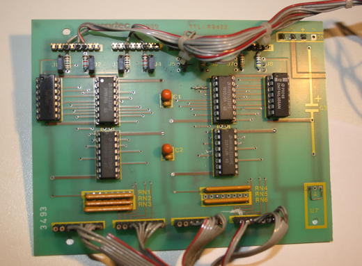
RS422_1

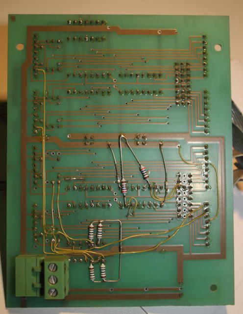
….and the back. A bit patched, some resistors added.

RS422_3

Those extra cables and resistors were retrofitted to allow the user to “partition” the x’plorer into either 1×16 or 2×8 Transputers. Therefore my x’plorer has a simple switch on its back to either select the full or half system. As there are 4 connectors in the back (2x TTL, 2x RS422) two users can use the system at the same time.

After removing the L-Shaped base from the main part, you can slide-out the blue side-panels leaving you with the dark grey frame holding the main circuit board… looking like this:
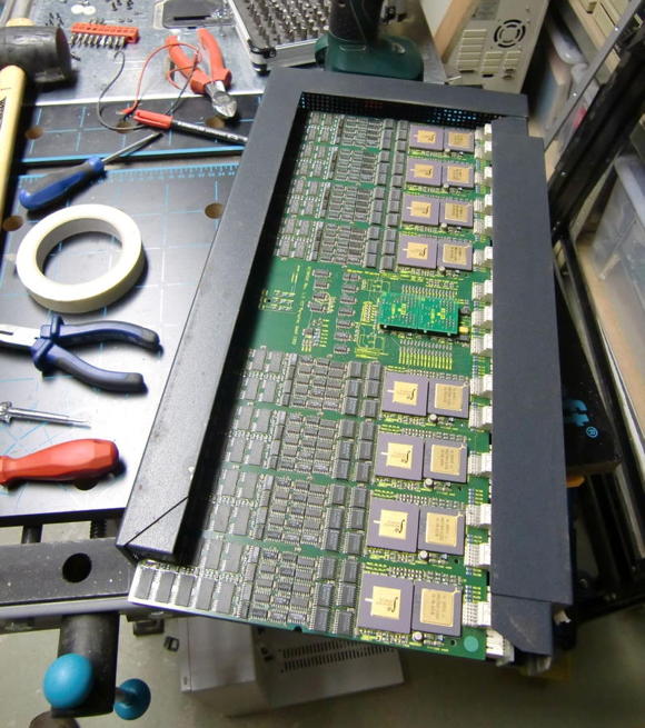
xPlorer_Workbench

You might wonder about the ‘workshop environment’ – well, actually you need quite some tools to open the x’plorer. Like with some Italian cars ;-), you need a different screwdriver for each screw. Here’s what I remember: Allen key size 2, 2.5 and 3. Also handy are a Torx size 3 and a Phillips size 2 as well a a rubber hammer to carefully removing the dark-grey frame (consists of 3 parts).
All in all, given the wild mixture of techniques and material used, I have the strange feeling that the x’plorer was created in a somewhat shirt-sleeve approach.

After some wiggling, careful knocking and a bit of cursing, you will have the main circuit-board laying in front of you – actually there are two boards, back-to-back, connected by a tiny backplane still hidden in the metal frame in the picture below.
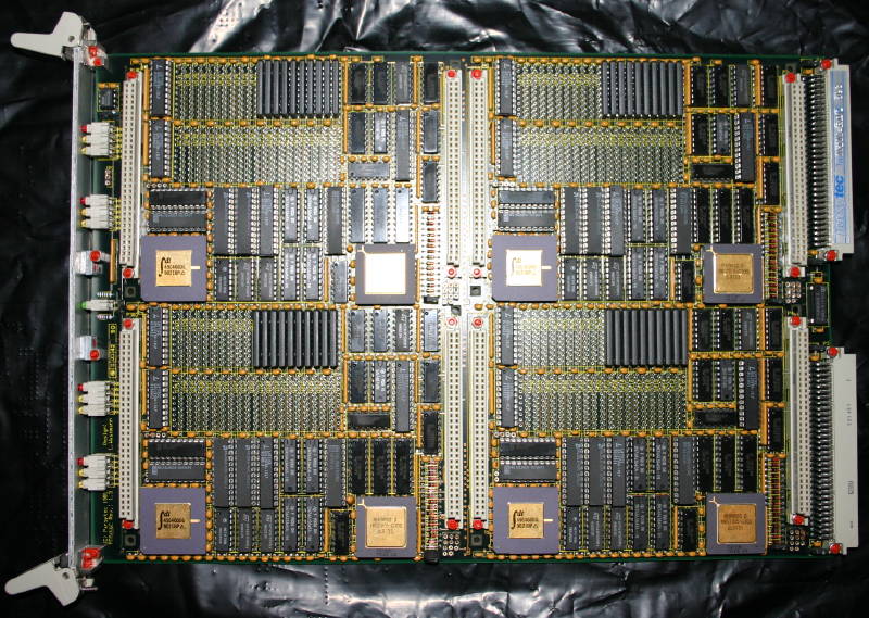
Definitely this is the high-tech part of the whole x’plorer using state-of-the-art technology of its time (1992):
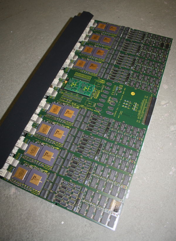
FullBoard

A closer look

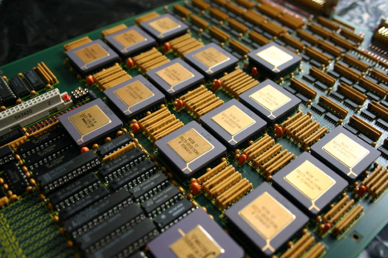
The boards layout is nice and clean. You can understand its design by simply looking at it – so let’s do so. Here’s a top-view of 3 ‘Blocks’ or ‘Columns’ as an example… all 16 look the same:
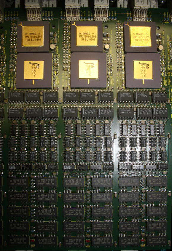
Topview_3_blocks

At the Top there’s the T805-30MHz Transputer. Right below is an IDT49C460 which is a 32-bit Error Detection and Correction chip which generates check bits on a 32-bit data field. Then there a lots of buffers and drivers which connect to the 4MB of RAM below them (80ns, so 4 cycle speed). Nice little feature: 2 SMD LEDs for error and running.

On each side, between 4 of those ‘blocks’ are two of those little circuit boards seated in 2 sockets (labelled ‘U1004’ and ‘U1005’). These are hard-wire replacements for the normally installed C004 link switches. Normally means if this cluster would have been installed in a GigaCube, there would be 4 C004s on each cluster allowing free and dynamic configuration of the Transputer network topology. So in an x’plorer you have to live with a fixed 4×4 network, which is not bad, because configuring 4 C004s can be painful 😉
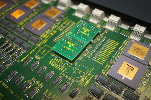
C004_dummies1

At the same spot, there’s a nice marking of the ‘fathers’ of this board, namely Mr. M.Vyskcocil and L. Wassmann.
Also, the official product name of this board is “GCT8PEDC” and it’s Revision 1.3.
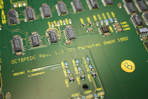
Model_GCT8PEDC

The “other x’plorer”

Well, yes, there was another x’plorer in existence. As with the GC-system, Parsytec later offered the “PowerXplorer”- you may guessed it already: It used the cluster from the PPC601 powered GC systems. I wrote a dedicated post over here about those hybrids, bastards, you-name-it 😉

Let’s roll

Now that we know what’s inside that beautiful case, let’s see if it’s still working. As mentioned before, Parsytec had a special way of resetting the Transputer(s). Instead of resetting all the Transputers in the network the same time (like INMOS did), Parsytec systems had been designed that each Transputer can reset its 4 direct neighbours. So you need to load a special software into a Transputer to do so.
That said, after powering-on the system, all Transputers will be reset automatically. This is the only chance to run standard Trasputer tools like ‘ispy’… once.

So I connected my trusty old Gerlach card to my selfbuilt RS422 interface and brought a cable from there into the x’plorer.
At its back, the x’plorer features four 8-pin sockets made by LEMO (Sockets are EGG.2B.308, so the plug might be FGG.2B.308 I guess) lloking like this:
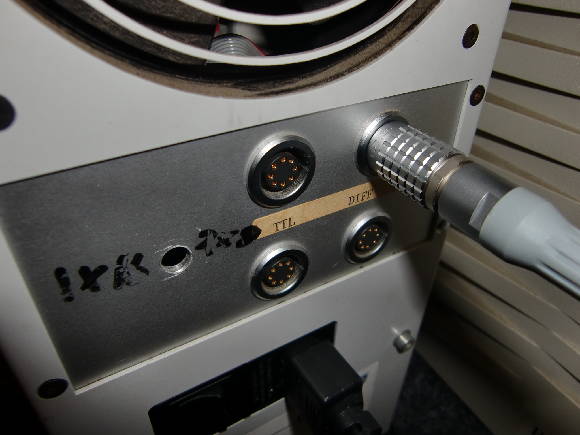
xpl_connectors


If you’re lucky enough to own one of those expensive plugs/cables, this is the wireing:

      1        1 Reset out+    2 Reset out-
   2     8     3 Link out+     4 link out-
  3       7    5 Link in-      6 Link in+
   4     6     7 Reset in-     8 Reset in+
      5

I you don’t have a LEMO plug, use the 2×5 sockets inside the x’plorer case right behind the LEMO sockets.  Their pin-out should be:

10  RO+  RO-  9
 8  LO+  LO-  7
 6  NC   NC   5
 4  LI-  LI+  3
 2  RI-  RI+  1

Now let’s call ispy and see what happens…

Using 150 ispy 3.23 | mtest 3.22
# Part rate Link# [  Link0  Link1  Link2  Link3 ] RAM,cycle
0 T800d-24 265k 0 [   HOST    1:0    ...    ... ] 4K,1 1024K,3;
1 T805d-30 1.3M 0 [    0:1    2:1    3:2    4:3 ] 4K,1 4092K,4.
2 T805d-30 1.8M 1 [    5:0    1:1    6:2    7:3 ] 4K,1 4092K,4.
3 T805d-30 1.8M 2 [    7:0    ...    1:2    8:3 ] 4K,1 4092K,4.
4 T805d-30 1.8M 3 [    6:0    ...    ...    1:3 ] 4K,1 4092K,4.
5 T805d-30 1.8M 0 [    2:0    9:1   10:2   11:3 ] 4K,1 4092K,4.
6 T805d-30 1.8M 2 [    4:0   11:1    2:2    ... ] 4K,1 4092K,4.
7 T805d-30 1.8M 3 [    3:0   10:1   12:2    2:3 ] 4K,1 4092K,4.
8 T805d-30 1.8M 3 [    ...   12:1    ...    3:3 ] 4K,1 4092K,4.
9 T805d-30 1.8M 1 [    ...    5:1   13:2   14:3 ] 4K,1 4092K,4.
10 T805d-30 1.8M 2 [   14:0    7:1    5:2   15:3 ] 4K,1 4092K,4.
11 T805d-30 1.8M 3 [   13:0    6:1    ...    5:3 ] 4K,1 4092K,4.
12 T805d-30 1.8M 2 [   15:0    8:1    7:2    ... ] 4K,1 4092K,4.
13 T805d-30 1.8M 2 [   11:0    ...    9:2    ... ] 4K,1 4092K,4.
14 T805d-30 1.8M 3 [   10:0    ...   16:2    9:3 ] 4K,1 4092K,4.
15 T805d-30 1.8M 3 [   12:0   16:1    ...   10:3 ] 4K,1 4092K,4.
16 T805d-30 1.8M 2 [    ...   15:1   14:2    ... ] 4K,1 4092K,4.

Tadaa! There they are: 16 30MHz Transputers running at full steam ahead! Some intense brain-boggling hours later, I was able to draw a “mesh-map”:

Host
|
4---1---3---8
|   |   |   |
6---2---7--12
|   |   |   |
11--5--10--15
|   |   |   |
13--9--14--16

After this ispy run you can’t reset the network again if you don’t use proper Parsytec tools… or Helios.

So quickly running the ispy output through my little Perl script (available in the Helios chapter on this page), some small adjustments and here it is, the Helios network map:

Network /Net {
Processor 00 { ~IO, ~01, , ; system; }
Processor IO { ~00; IO; }
{
Reset { driver; ; pa_ra.d }
processor 01 { ~00, ~02, ~03, ~04; }
processor 02 { ~05, ~01, ~06, ~07; }
processor 03 { ~07,    , ~01, ~08; }
processor 04 { ~06,    ,    , ~01; }
processor 05 { ~02, ~09, ~10, ~11; }
processor 06 { ~04, ~11, ~02,    ; }
processor 07 { ~03, ~10, ~12, ~02; }
processor 08 {    , ~12,    , ~03; }
processor 09 {    , ~05, ~13, ~14; }
processor 10 { ~14, ~07, ~05, ~15; }
processor 11 { ~13, ~06,    , ~05; }
processor 12 { ~15, ~08, ~07,    ; }
processor 13 { ~11,    , ~09,    ; }
processor 14 { ~10,    , ~16, ~09; }
processor 15 { ~12, ~16,    , ~10; }
processor 16 {    , ~15, ~14,    ; }
}
}

Obviously you have to ‘compile’ a .map file out of that and adjust your initrc file – all this is described in the above mentioned Helios chapter.
When you have done everything correctly, Helios will happily boot your x’plorer and you can enjoy the mighty power of 16 (well, 17) Transputers!

Olivetti CP486

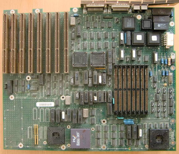
The Olivetti CP486 was “the other” machine on the market which provided an 80486 and an 80860 on the same mainboard. The same board was used in Olivetti machines called LSX-5010 (25MHz) or LSX-5020(33MHz).
Like the Hauppauge 4860, it was an EISA bus system too, had no 2nd level cache but an extra socket for a Weitek 4167 FPU. Again very similar is the use of an huge array of PALs and GALs… and huge is the keyword for its size:  40,5 cm x 34 cm (16″ x 13.4″)!

CP486_total

My CP486 which I’m showing here seemed to have been through very though conditions. It was quite dirty and is of course not working :-/ Mainly due to a missing PAL, I guess (shown in the following picture).
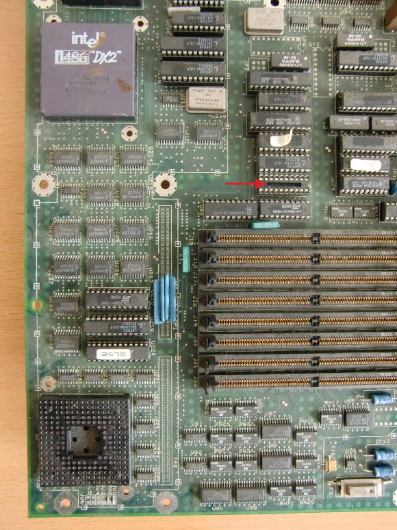
So here’s the lower part of the board (90° tilted for better reading):

CP486_left

At the top the i486, in this case an DX2/50 I had lying around – nicely fitting the 25MHz oscillator to the right of it. At the edge of the photo you can see a bit of another socket. That’s where the optional Weitek FPU would have go (See the picture of the total view).
Next you’ll spot the many PALs around it. And a wild mixture it is! All PALs/GALs on the board are from different manufacturers, years and kinds. Some still featuring labels, most of them peeling off. According to the only documentation I was able to find, “in field” upgrades seemed to happen quite often. The little red arrow indicates the missing PAL at “U82” I talked about before. It should be a 16R4 containing the snoop-control, a vital part of the memory management. Without it, the board is pretty much brain-dead 🙁
Next are 8 slots for PS/2 SIMMs… depending on the BIOS version up to 64MB RAM were usable.

In the low left corner is what made this board special: The i860 socket. The 3 PALs above it are his address decoders… nothing is known about how the two processors shared the RAM.

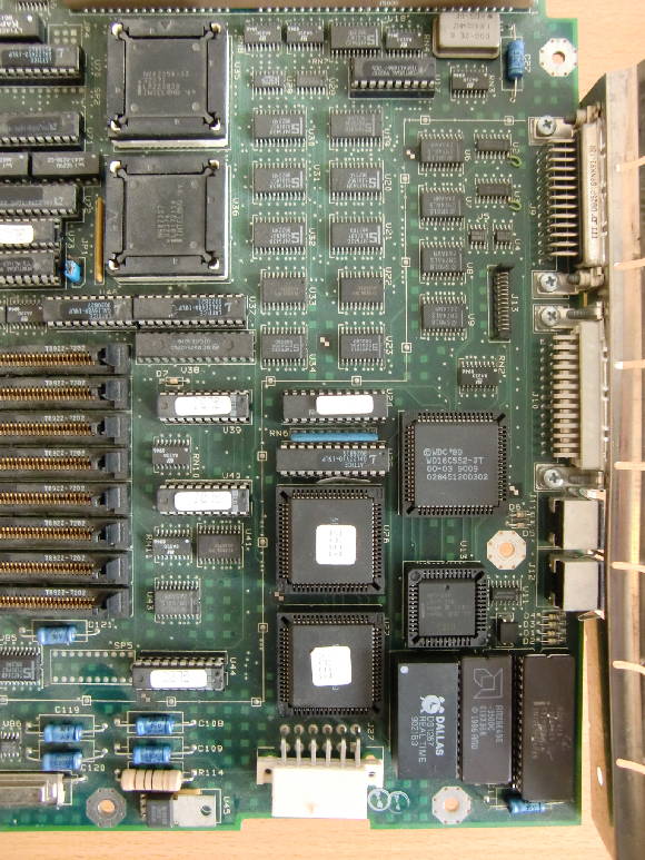
Which leads us to the other half of the board:

CP486_right

This part is mainly chip-set stuff. At the top left there are the Intel 82358 EBC and 82537 ISP (See my Knowledge-Base article for more info) ICs.
The rest of the action is squeezing into the lower right corner: On top the WD16C552 Serial and Parallel Port Controller. The other two bigger PLCC ICs are EP1800 CPLDs supposedly working as I/O controllers. To their right is a 8742AH handling the PS/2 keyboard and mouse.
Below that there’s the inevitable DALLAS clockchip, a 64kbit EEPROM (probably EISA config) and a 1Mbit 28F010 Flash EPROM for the BIOS. Pretty modern stuff actually.
Naturally I read out the BIOS… it’s completely Olivetti propriety as they always did back in those days (Download available at the end of this page).
Last but not least, the power connector. Again, propriety but I do have the original power supply. Nice big paper weight.

The EVC-1

Like the Hauppauge 4860 (again), the CP486 also offered a special Graphics Card which enabled the i860 to directly write into its video memory, so it could be used as an accelerator.
While Hauppauge went the way of offering a special dedicated slot, Olivetti designed a special EISA Video Card… well, the EVC-1.

CP486_EVC

While it features a standard EISA slot connector, it does not work in other EISA systems (You get the BIOS boot messages but it then hangs with wire-do chars displayed).

It’s core is a Chips & Technologies 82C452, a mediocre VGA chip.  Olivetti attached this DRAM VGA controller to 1MB dual-ported DRAM… This totally makes sense because the 82C452 can act as a simple VGA controller while the i860 will als be able to write to the screen (via EISA DMA) for example doing the heavy lifting graphics stuff. The idea is the same as Hauppauges Framebuffer but enhanced with a VGA controller.
That said, IMHO 1MB video memory is a bit less for such a professional approach.

Conclusion

So, here‘s the CP486 PDF-document I was able to find in the WWW including my BIOS dump.
If you happen to own a CP486/LSX50x0 I would be happy to hear from you!
Final anecdote: I’m not sure this guy (German forum, Google-Translate will most likely help) knew what he was doing when scavenging a complete, fine running LSX-5020 for a boring case-modding stunt. In a few years he will kick his ass for killing a one-of-a-kind machine for a boring mass-market PC.
That’s the same sin many Americans did to their vintage Ferraris when they replaced the somewhat complicated original engine with an off the shelf Ford V8 to make it reliable… and reduced its value to 10%. Sin! Sin I said!

Frankenpal

This is a hack which is very similar to the DesperRAM. It was born out of pure despair, so it’s neither elegant nor very clever – but it works and that’s what counts.

During the “BOZO resurrection“, I had one specific PAL under suspicion to not working correctly any more. That PAL was soldered (i.e. not socketed) onto the board in a very tight spot, so I wasn’t able to cut the pins as close as possible down on the board.
I know, there are special pliers which can somewhat around corners, but my trustworthy Knipex (The pliers maker in the world, full stop.) can’t. So I had to cut the pins right at the PALs package – easy and quick.

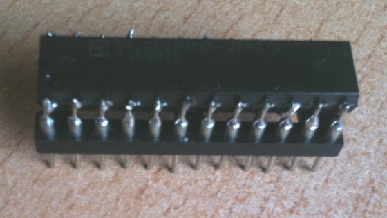
The downside is that this method leaves you with a leg-less IC… and if you then decide it might be useful to read-out that IC (like I did) it’s time to slap your forehead :-/
But not so fast, young Padawan. Despair has the advantage that it normally can’t get worse, so nothing to lose. Even you cut the legs off you still can spot the tiny remains leading into the package. So why not trying to replace the amputated legs with artificial limbs!?

My initial thought was soldering new pins to the package, but the remaining connection is way too small to allow anything to be soldered to it but a human hair.
So I used a socket, turned upside-down, slightly bent the legs inward, squeezed the PAL between the sockets legs and carefully soldered the pins to the case-connectors. Finally I put small bits of wire into the sockets empty holes to create new pins to connect the whole thing to my GAL-programmer. Voilá: FrankenPAL

FrankenPAL

Yes, it looks horrible and I was quite sure that this doesn’t work but it just costed me 10 minutes, so what the heck, let’s try read-out that beast.

What should I say? It worked right on the first try… So never despair as long as you have a working solder iron 😉

The Inmos B020

Well, normally I wouldn’t list Inmos’ expansion cards here, as they’re normally just TRAM carrier boards and very well documented at the usual places… but for this card, it’s different.

Not only that there isn’t any documentation of the IMSB020 (just a brochure over at Rams page) but this specific card is an updated version of that described in the brochure… I’d call it Rev.2.
It has a T805 instead of a T4xx and probably some more additions…

Ok, first of all: What is the Inmos B020 anyway? It’s being sold as a “X11 server on a card”… I’m intentionally writing ‘being sold’ because that just one way of usage.
More generally spoken, it’s an ISA card with a Transputer (with 4-12MB RAM) and a graphics controller on it, an Inmos G332 to be precise. That Transputer controls the G322 and can therefore create graphics onto a VGA screen connected to the board.

As an avid reader of GeekDot, this should sound familiar to you because it was the typical 90’s approach of High-End Graphics… see the MiroTiger or the SPEA i860 boards.

With the right software being booted into the Transputer, it may act as a X11 (R4) Server… but it could also used as a native Transputer system, e.g. running Helios or some OCCAM code and still create graphics with the G332 controller. As a nice add-on, the card features two size-2 TRAM slots, so more transputers or devices could be added into the equation.
Ah -and as a side note- most people called the B020 “the BOZO“… not very kind but it gets a credit for its pre-l33tc0de usage.

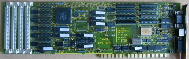
This is how my ‘rev.2’ looks in it’s full glory:

B020full_small

As usual, we go into more detail looking at each half of the card.In this full-view, you can identify the two TRAM-slots by the yellow markings at the lower edge of the card saying “SLOT 0” and “SLOT 1”.

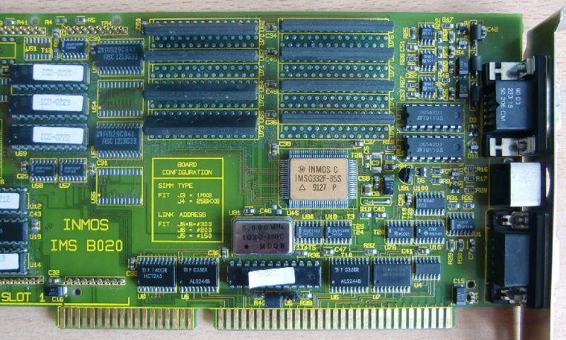
So let’s start with the right half of the B020:

B020right

At the right-most edge, there’s the VGA-in and VGA-out connector, so that you can loop-through the video signal from your regular graphics-cards (a fancy ET4000 for example ;-)).

Between the two VGA connectors is an 8-pin Mini-DIN connector, which has this pinout:

1 Error/ (in)
2 Analyse (out)
3 Tram2 Link 2 out
4 Ground
5 Tram2 Link 2 in
6 Onboard T800 link1 out
7 Reset (out)
8 Onboard T800 link 1 in

The upper 2/3, starting with the golden IC (IMSG322F-85F) is all graphics part. Which consists of the G322 controller, 1MB VRAMabove him and some latches and 3 PALs on the left of it.
Below the G322, next to the slot-connector is the ISA interface. That’s handled by a PAL (with the sticker peeling off) and 4 buffers/transceivers and a bit more “chicken food” around them.
Of course there’s also the inevitable 5MHz oscillator which is needed in every Transputer household.

Let’s move to the left half of the card:

B020left

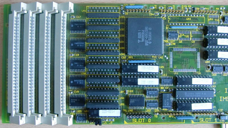
This is ‘where the music plays’. At the lower edge of the right side you can spot the C012 guarded by two PALs (with white labels) who handles the ‘Bus data-to-Transputer’ translation. The two PALs are most likely the subsystem (i.e. handling Reset, Error, the 012’s RS0/1 registers etc.).
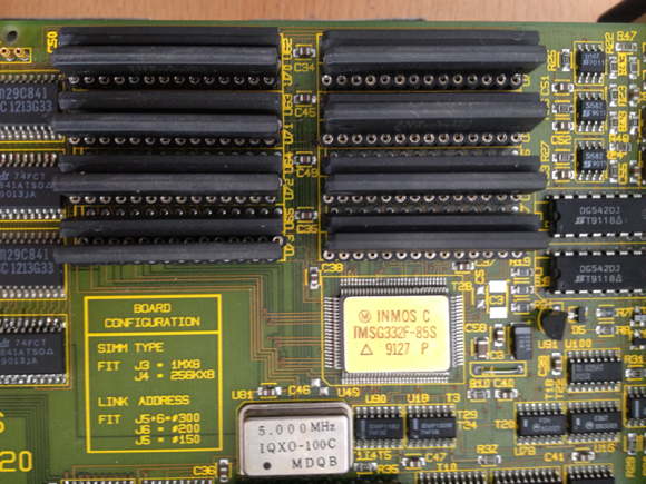
Then there is the King of the Hill, the Transputer himself – a T805-25 in a quite rare PLCC packaging. To his left are 4MB of RAM in ZIP-packaging, most likely configured and controlled by the two PALs below him.
Finally, there are 4 SIMM slots to expand the Transputer memory further to a whopping 8MB! As you can easily see, there are unpopulated solder-pads between the ZIP-RAM ICs (as well as the VRAMs). My assumption is that you could order this card with 8MB soldered, which lead to a max. RAM of 12MB, like mentioned in the brochure on Rams page. But I fear the PALs of the RAM-subsystem need to be programmed accordingly to support the larger amount of RAM (added later: And boy was I right!).

So much for the theory of the B020… and it might stay so for some time, because my B020 is was broken 🙁

But I’m working on it and one fine day you will see an X11 server in an XT-PC at blazing speed 🙂

B020LA

Resurrection

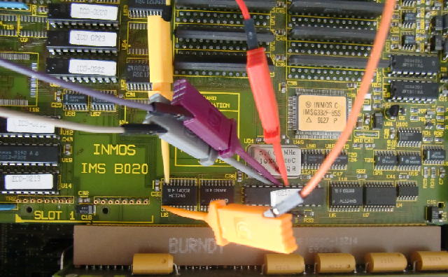
[Nearly 4 weeks later…] As promised, I worked hard on getting the BOZO back to life. It started with weeks of tracing connections of the complete bus-interface, ie. ISA-Bus to the buffers/transceivers, the PAL next to the ISA-bus, the C012 link-adapter etc.etc…
Then, knowing the signals now, came days of staring at the logic analyser, many many mails with Mike Brüstle and lots of hacking with DOSes debug.exe.
Finally it became clear that the PAL 0211 was somehow “confused” and therefore not controlling the bus as it should do. Because there’s no documentation neither of the B020 nor of its PAL equations (like there is for e.g. the B008) I had to go the long and bitter route of reverse-engineering.

So first thing is to remove the faulty part which proved to by a bit tricky – which is a short story of its own available in the DIY-section of this page.
So in went a proper socket and a copy of the original PAL (now a “modern” GAL). The copy proved to be a 100% one… which means not working as it should. But somewhat different than the tries I did before…it was erratic. For example only on I/O port 0x200 I was able to get something useful out of the signals (eg. a well timed /OE for the ‘244 buffers) while jumpering the IO range to 0x150 or 0x300 gave total silence. So I went one step closer to the bus, listening to what the PAL gets on its A4-A11 lines.
There you go! A4-A6 were constantly high and A7 glitching while A8-A11 was happily bouncing. According to my tracing A4-A7 were handled by a different ‘244 than those working. So Sauron turned his eye on the little SMD octal buffers… out went the solder iron and all pins of all buffers were re-soldered.

Lo and behold, the next ispy run on 0x200 worked! Heureka!

Next up: Why is it working on port 0x200 only? Learning from the ‘244 issue I checked all solder-pads concerning the jumper for port 0x150 (that’s J5). Everyhing looked nice and re-soldering didn’t change a bit. So it was the PAL who was suspicious… again.
Luckily INMOS refrained from setting the protection fuse on the PAL, so not only I was able to copy it but also the read its programming. I was thinking about recoding the whole thing and started doing so when I stumbled across a missing “.oe” (Output Enable) for exactly that input-pin connceted to the J5 jumper. So quickly adding

/f14 = gnd
f14.oe = gnd

to the code, compile, burn, plug it into the socket. Tadaa! The B020 now also talks to 0x150… and 0x300 respectively.
[BTW: This happened right at the 30th birthday of DOS. Don’t know if it’s a good or bad sign… at least DOS is my favourite debugging tool 😉 ]

For those who happen to have the same issues with their B020 (erm, that’s probably 1-2 people on this planet by now), here’s my documentation and .jed file for the “PAL 0211B”.

Enhancement

Well, as said in Axels 10 commandments: “Thou should not leave a socket unpopulated!”
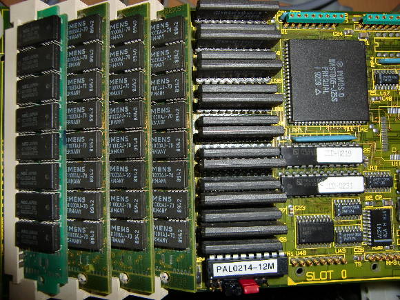
And my B020 has a lot of ’em. So I started with the Transputer RAM.
In preparation I checked if the empty solderpads (as you can see in the above pictures) do get all the required signals… well, kind of: I was lazy and just checked /OE with my logic analyser and there was a signal in sync with the one of the already installed RAM. Also all Data- and Addresslines were connected… so it was worth a try!

But I should have known it before: After clearing all 160 pin-holes from the solder, puting self-made zig-zag sockets in place and filling them with the appropriate 1Mx4 RAM chips ispy/mtest still reported just 4MB of RAM :-/

Obviously PAL0214, sitting right below the ZIP RAM was playing an important role here. So the good old routine of “buzzing it through” began. After 2 days I pretty much figured out the purpose of each pin of PAL0214. Yes, it must be the RAM decoder.
So there was no way around removing, reading and replacing it… like with PAL0211.
This time I got myself a desolder-gun – a hell of a facilitation! Again, luckily the PAL wasn’t protected so reading it wasn’t an issue.
As expected, the decoding for the 2nd RAM bank was missing – no idea where the initial measured /OE signals came from.
After the decoding of 1st 4MB ZIP RAM the SIMM RAM followed immediately – so I had to squeeze in the 2nd bank of 4MB ZIP RAM and let the SIMM RAM follow after that. Even my VHDL/PAL Equation skills are quite limited it wasn’t as hard as I expected. Compile, program, put the new GAL16V8 in place, start ispy/mtest, cross fingers….

Using 150 ispy 3.23 | mtest 3.22
# Part rate Link# [  Link0  Link1  Link2  Link3 ] RAM,cycle
0 T805d-25 340k 0 [   HOST    ...    ...    ... ] 4K,1 12284K,4;

Yay! 12MB including the SIMM RAM!! Here’s the view of a “BOZO to the MAX” 😉

BOZO_full_RAM

Double the VRAM!

The last step in bringing the BOZO “to the max” was adding more VRAM, i.e. 2MB.
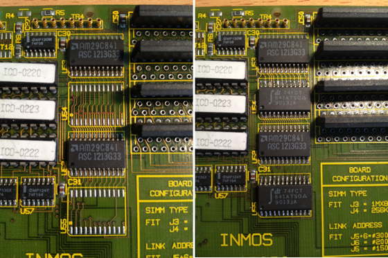
So first you have to get two more AM29C841 9-bit latches (or compatible parts, like those 74FCT841 I’ve used) in SO-24 package. That SMD package is still quite easy to solder onto the board. Here’s a before-and-after picture:

BOZO_VRAM1

On the right-hand side of the latches you can already spot the empty solder-holes for the VRAM. Like with the DRAM expansion before, I made my own sockets by using two 1×14 pin sockets. This is what the now fully populated VRAM section looks afterwards:

BOZO_VRAM2

The first run using “ixcheck” from the INMOS iX package went without errors and the /OE signals of all the ‘841s are driven correctly according to my logic analyzer. I was a bit scared that INMOS might have again not completely programmed the PALs (left to the latches) to support this memory expansion but it seems I’ve been lucky.

Next up: Find a tool using the 2MB and confirming that the extra VRAM is actually usable.

Inmos TRAMs

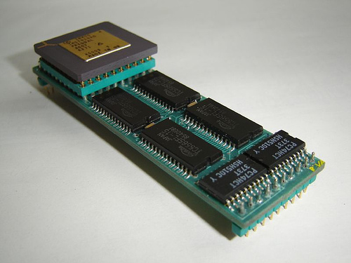
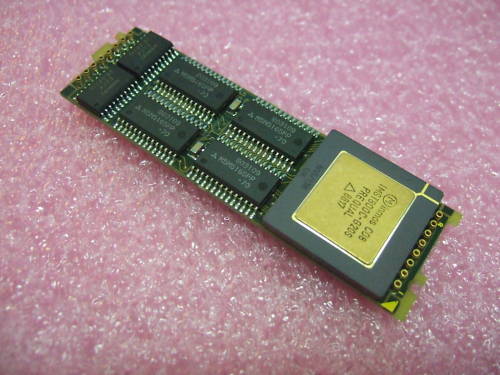
INMOS was obviously the first manufacturer of TRAMs. Over the time you can clearly see the progress the technology made over the period Inmos TRAMs were made. Starting with comparably big sizes, using DIP chips etc. the last of its breed were highly integrated PCBs cramped with SMD parts and chips.

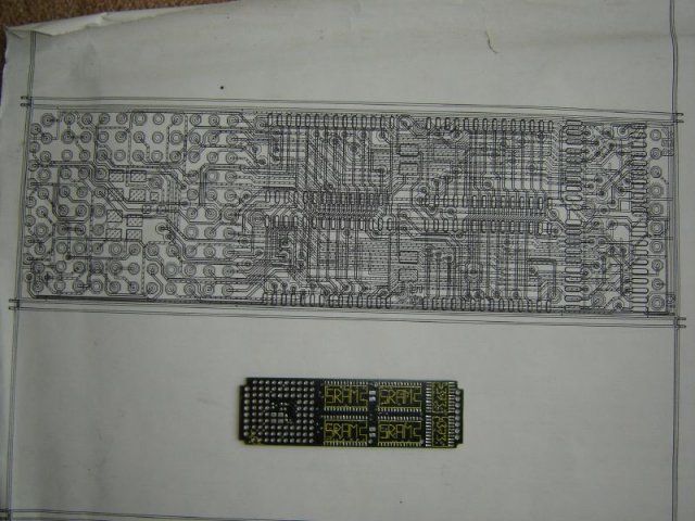
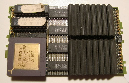
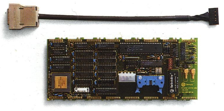
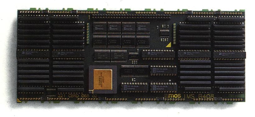
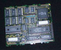
The IMS B401 started it all. A 32KB SRAM size-1 TRAM for a 32-bit Transputer. Here’s the prototype, the final product and a picture of its schematic:

B401_Layout

The “huge” IMS B403 1Mbyte DRAM Size-4 TRAM:

IMSB403_1

The IMS B404 (2MB DRAM, Size-2) is where the fun starts. Size-2 is just OK not to totally hog your mainboard and 2MB is what you need for OCCAM or HELIOS to make something useful.
Actually, the B404 has 3 “levels” of RAM. 4K internally in the Transputer, 32K SRAM and 2048K DRAM. As they are superimposed (i.e. overlapping), the total amount is still 2MB with different access speed at 0-4k (1 cycle), 5-32k (3 cycles) and 4-5 cycles above.

IMSB404

There were also the IMSB402 (8Kbyte Size-1) and the IMSB405 8Mbyte Size-8 TRAMs of which I have no pictures yet.

The IMS B407 was an Ethernet TRAM (Size-8!), proving that a TRAM doesn’t need to be necessarily a Transputer Module for number crunching only.

imsb407

The IMS B408 and B409 were both part of a graphics system, so you didn’t the to have the host to render the graphics – which would have been much slower than those TRAMs.
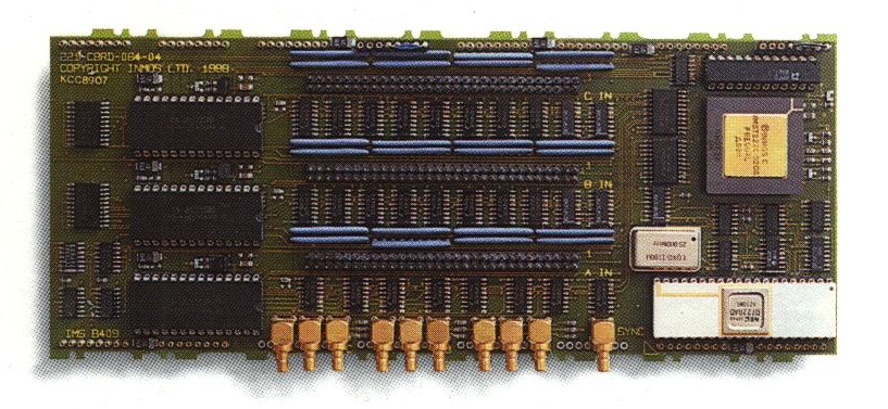
The B408 was the “drawing pad image storage” (1,25MB dual-ported RAM), while the B409 had the timing generator and the CLUTs:

imsb408

imsb409

The IMS B411 can be seen as a new era: 1MB DRAM on just a size-1 TRAM made possible by the use of small ZIP-packaged DRAMs… which were very expensive, of course.

IMSB411-3B

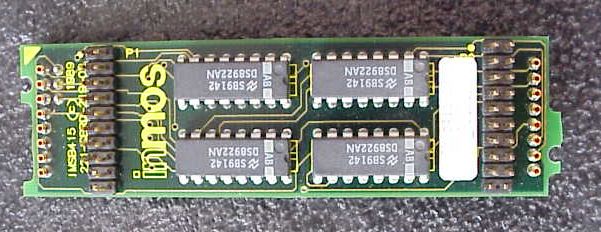
The IMS B415 is a simple Transputer-Link to RS422 converter. This way, link connections can span up to 30 meters.

imsb415

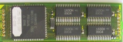
The IMS B416 features a 16bit T2xx Transputer and 64KB SRAM

IMSB416_10P

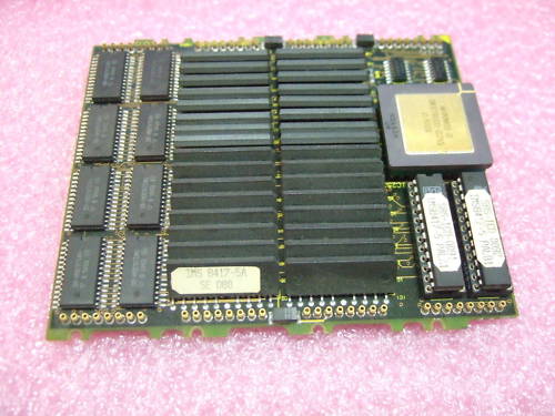
The IMS B417 is a massive beast: 4MB on a size-4 TRAM… well, still better than the B403.

IMSB417-5A

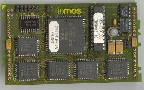
The IMS B418 contains a 16-bit T222 and 256KB Flash ROM… quite modern stuff those days and probably a good way to boot your HELIOS system from 😉

IMSB418_1

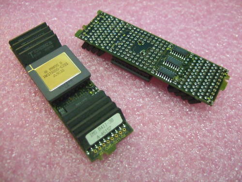
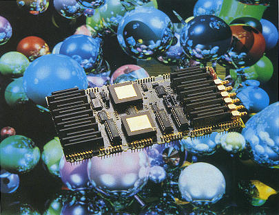
The IMS B419 combined the two huge B408 and B409 modules into one size-6 TRAM. A nice graphics TRAM with 2MB DRAM and 2MB VRAM…

imsb419

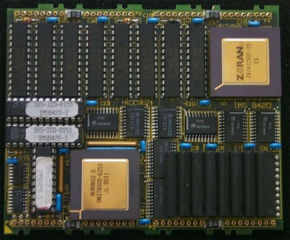
The IMS B420 featured a ZORAN ZR34325 DSP (45 MFLOPS peak) with its own 256KB SRAM besides the obvious T800 Transputer and 4MB DRAM. My guess is, that it is comparable to the Quintek QVA-T TRAM.

imsb420_1

The IMS B421 enabled a Transputer system to talk to GPI/IEEE-488 buses … like laboratory equipment or your old Commodore Floppydrive 😉

IMSB421_1

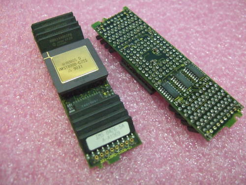
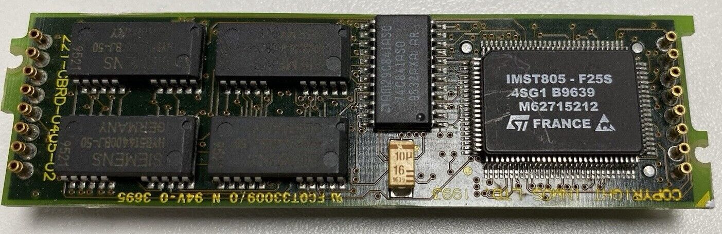
Ahh, the real-deal… the IMS B426 is what you want in your TRAM collection. 4MB RAM on a size-1 TRAM. This is where Helios really loves to run on.

IMSB426-5A

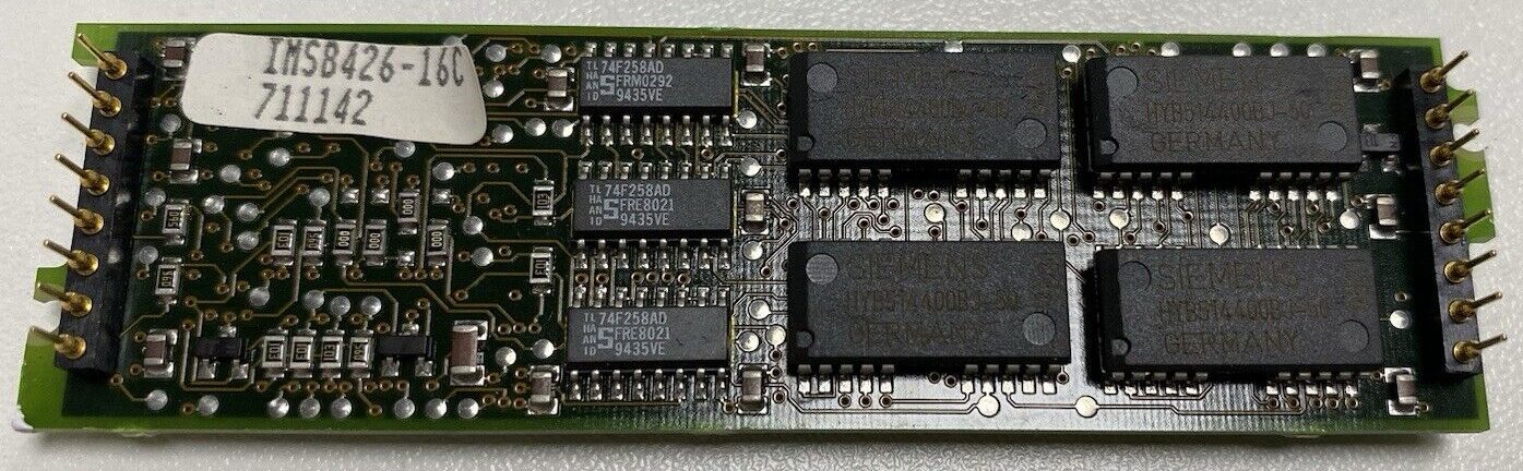
…and here’s a more recent version of the B426 (rev “-16C”, 1993), this time all SMD, featuring the latest T800 in a nice TQFP case

Well, the IMS B426 is great… as long as you can’t get the IMS B427 😉 This Size-2 TRAM features a whopping 8MB RAM. Enough for running Helios and X11 on it.

IMSB427

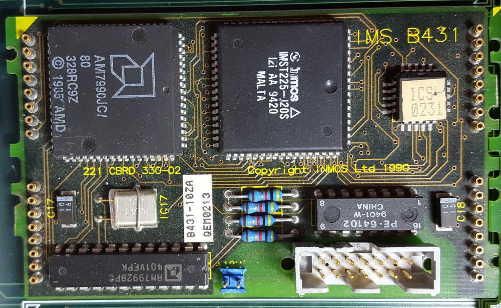
Something more important than ever is a fast network connection. The last ethernet TRAM from INMOS was the IMS B431.
10mbps is the maximum you get… well, more wouldn’t make sense given the Linkspeed of 20mbps.

IMSB431

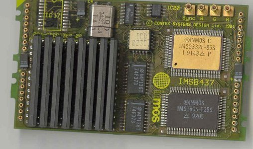
The IMS B437 is a very neat little thing: A graphics TRAM as size-2 TRAM! A nice 25MHz SMD T805 and a G332 colo(u)r video controller. Rare as chicken teeth!
It looks like this was designed by Contex Systems Design Ltd. and OEM’ed by INMOS.

IMSB437_1

And when you thought you’ve seen them all, another one pops up:
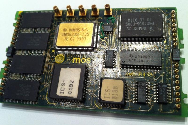
The mighty IMS B438. As the name-code suggests, it’s an updated B437 – very updated and IMHO the ultimate graphics TRAM: 2MB VRAM, 4MB DRAM, 30MHz T805 and the last and final 32Bit video controller G335@130MHz. I really, really want one. Badly!

B438

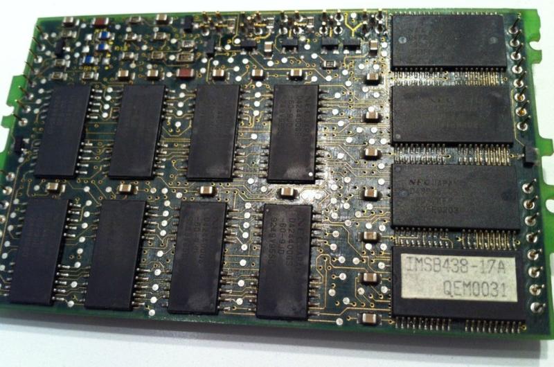
Because it’s a beauty, here’s its back, too:

B438_back

The SPEA Panther

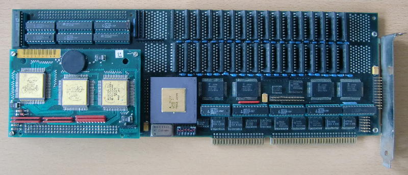
This is really a rare breed… and yet another “cat of prey card” to be flopped: The SPEA Panther.

panther_full

Basically, it’s an Intergraph Clipper workstation on an ISA-Card. As usual, you can find more details about Intergraph and the Clipper CPU architecture elsewhere.

Most likely built & released 1988, this full-size ISA board features a Clipper C100 CPU(set), 4MB of ram (expandable to 8MB) and quite some glue-logic, mostly buffers, lots of GALs, some DP-RAM – and sad enough: no EPROM.
Having no EPROM means it was “booted” by the hosting PC and there’s no clue of how to feed this beast, i.e. what kind of protocol it is talking to the ISA bus.

A german article in the endless archives of “Computer Woche” (21.10.1988) mentions this:

[…]Für den SPEA-Panther, einem Aufrüstungsboard für PC, steht jetzt die CAD-Software Intergraph Microstation zur Verfügung. Besonderes Merkmal dieser Software ist, daß der Kern unter Unix läuft, die Anwenderschnittstelle jedoch eine DOS-Lösung beinhaltet. Microstation liest und schreibt DOS-Files. Auf Grund der Lösung “Unix under DOS” ist die SPEA-Version von Microstation voll kompatibel zu Workstations.” (Source)

Translated:

“[…]For the SPEA-Panther, a PC expansion card, Intergaph’s CAD-Software Microstation is available now. The particular feature of this software is that its core runs on UNIX while the user-interface is still hosted on DOS. Mircostation reads and writes DOS-Files. Because of the “Unix under DOS” solution the SPEA-version of Microstation is fully compatible to the workstation [version]”

So the Panther was probably running a full version of CLIX, Intergraph’s version of UNIX and the x86-Host was degraded to be the terminal… given the 1988 speed of PCs (Compaq just introduced the DeskPro 386 @ 16MHz), not the worst idea to have.
Well, if it wouldn’t to be the case that the Clipper architecture itself was dying a slow death over the next 2 years…and Autodesks AutoCAD was getting faster as 386/486’s were taking off…

That’s probably the reason why there’s next-to-none info about this card on the web… and print and newsgroups: Too expensive, too specialized, just a hand-full sold.

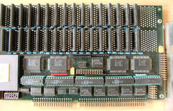
So just for the fun of it, here are some more detailed pictures of this “one of a kind”. The right half of the card has the ISA bus interface, four chips from Fujitsu marked MB622202 (my guess is it’s Dual Ported RAM), lots of 81C4256 DRAMs (32, so 4MB) and a mysterious gold-lid PGA Fujitsu chip marked C143C1C and 76460… could be anything. Ah, and a dip-switch… most likely for setting the I/O address or IRQ.

panther_right

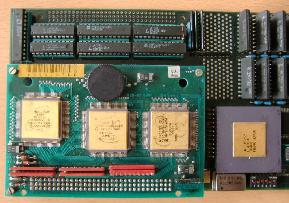
The left side of the card is dominated by the CPU daughter board, obviously provided by Intergraph itself (featuring the companies logo) as I had seen this kind of board before. Above the CPU are even more PAL/GAL chip.
And again, the unknown C143C1C chip, now in its full glory. Next to the chip a 60MHz oscillator which lets me guess that the C100 runs at 30MHz… a bit below standard for C100s.

panther_left

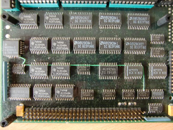
When buying the card my hope was that there might be more enlightening stuff below the CPU daughter-card. But as most times in life… there was nothing worthwhile 😉

panther_below_CPU

Just lots of TTL logic and buffers… the PLCC on the left is a N82C54… a CHMOS programmable interval timer… boring.

So to conclude this chapter, I guess I won’t make this card run again – ever. It’s just another example of how undecided the computing world was around 1988. There where more than one way to reach your target (speed) but most of them failed. Still I think it was much cooler than today.

Update 2016:

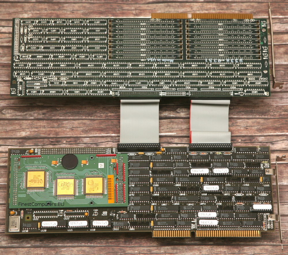
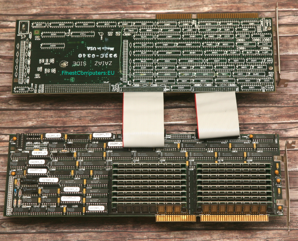
Found an interesting auction on ePay… this is the original Clipper card – which seems to be the “blueprint” for the Panther… SPEA just replaced the tons of discrete logic by some ASIC chips, which made room for RAM. On the  original cards that is placed on a separate daughter-card:
(Pictures courtesy of FinestComputers.eu)

Clipper_total_f

The CPU card back side and RAM card front:

Clipper_total_b

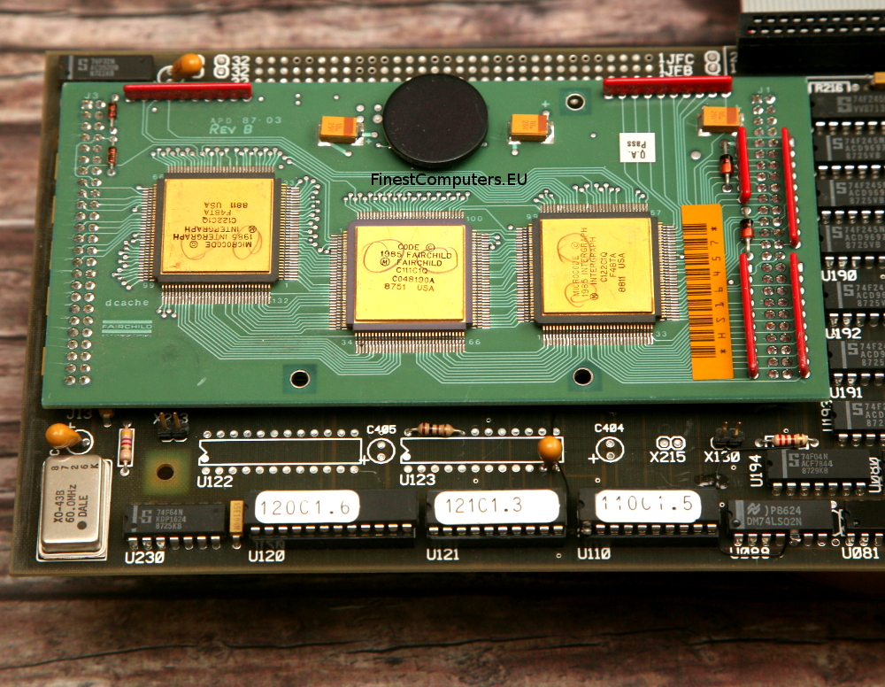
The CPU Module is the same as used by SPEA:

Clipper_detail