All posts by Axel

http://www.geekdot.com/about-me/

The T9000

Again, Geekdot.com might be the only place left in the World Wide Web where you can get more information about the flopped mysterious T9000 than what you will find on Wikipedia.

The T9000 never made it into the market in higher volumes. I don’t have any numbers on how many T9000 were actually produced but only a few were evaluated outside INMOS by universities and science facilities, most famous is probably the CERN, which did some benchmarks and tests. Here’s a (now funny) promotion video of those days:

By another lucky incident I got myself a HTRAM mainboard for Christmas 2011. It’s the QT9M from Quintek, a spin-off of INMOS back then. Three slots of this 6-slot board were populated, one featuring the mythical T9000!

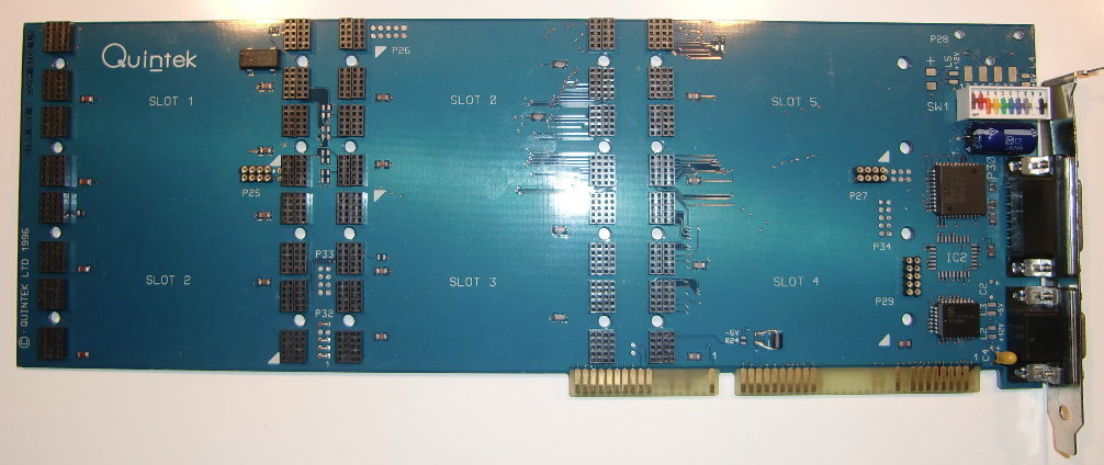
This is the naked board, the QT9M:
QT9M_total

At the first look you can see it’s a damn huge thing. At least one inch taller than the slot-backplate. But this way Quintek could squeeze 6 size-1 HTRAM slots (3×2 slots, horizontally) onto the card, while the “official” INMOS B108 (PDF) board just features 2 slots (but size-4, vertically).

The HTRAM slots in detail

(-> For a complete description of HTRAM visit this chapter of geekdot.com)

Not all slots are offering the same features, though. Slot-0, slot 3 (the two middle ones) and slot-2 (lower left) offer the standard pin-blocks 1 and 2 as well as block 3 and 4.
slot-1 (top-left) offers the same pin-blocks but also a small 4×2 horizontally aligned block on its lower edge.
The same 4×2 pin-block can be found on HTRAM-slot 5 (upper right), but this time only the standard pin-blocks 3 and 4 are featured.
Finally, on slot-4 (lower right) only the standard pin-blocks 3 and 4 are featured, too, but it also has a 5×2 pin-block centred to the opposing edge of the standard pin-blocks.
My assumption is that pin-blocks 3 & 4 offer a direct connection into the T9000 memory map, so I’d call slot-4 & 5 “mem-mapped-ony slots”.

The interface logic

The interface logic on the board was kept surprisingly simple. Especially when you compare it to the already mentioned IMS B108, which had an FPGA and two C101 protocol converters.
Without any C101 you can be assure that there won’t be any downward compatible communication as we are used to with the T4xx/T8xx Transputers (OS-Link), so this will be a hard nut to crack :-/

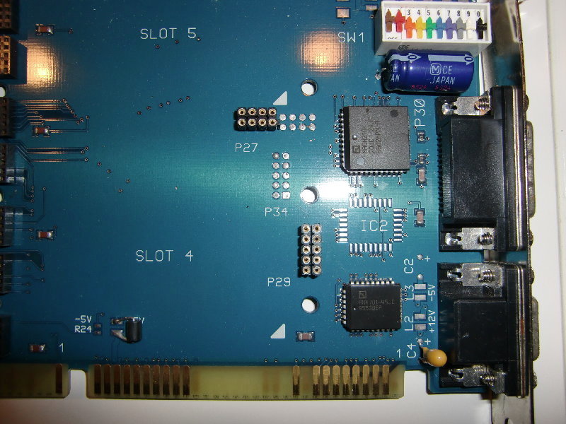
Let’s have a closer look at the “logic side of things”:
QT9M_detail

There are only 2 ICs: An AMD MACH 210 CPLD and an AMD 4701, which is an 8-bit bi-directional 512 byte deep FiFo Buffer and parity-generator. Given the fact that there’s a place left for IC2, I assume a 2nd 4701 could go there to make the interface 16bit wide (as all 16 ISA data-lines are connected on the slot-connector).

This leads to my totally uneducated guesses, that:

  • The DS data-links are directly connected (through the FiFo) to the ISA bus
  • The control registers of the AM7401 needs to be set – if the default state is not sufficient

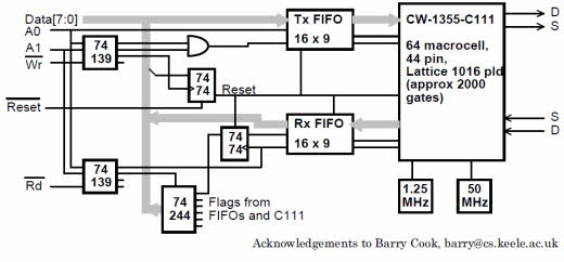
Quite a solid foundation to those assumptions is the following schematic I was able to dig out of the depth of the internet describing an IEEE 1355 interface. IEEE 1355 is the standard which was created out of INMOS’ DS-Links.
DS-Link_CPLD

Everything else…

The function of the colourful DIP-Switch is yet completely unknown. It’s clear that some of these switches will set the base-address for communication with the ISA bus.
The sense behind the two Sub-D connectors at the cards backplate are unknown, too. Maybe some link-outs?

(To be continued…)
Run Forest, run!

After having figured out the basics, it was time to prove the concept. First, I needed a (simple) program to run on the NumberSmasher. Here it is, reeeeally simple. It’s just an excerpt of the original 77 assembly lines. If you’re interested in the whole thing, it’s here.

The main-loop is just this. Read a byte from the C012 link, add 1 to it and write it back to the C012:

mov    iobase, %r4

loop:
  call    getlink        # (watch following delay slot!)
   shl    %r0, %r4, %r16    # mov r4, r16 - save base address

  addu    1, %r16, %r17    # add 1 and move into r17

  call    putlink        # (watch following delay slot!)
   shl    %r0, %r4, %r16    # mov r4, r16 - save base address

  br        loop
nop

What a task for a “Cray on a chip”! 😉 Ok, putting this into the assembler (currently gnu-as on Linux), linking and finally making it a pure binary with ‘objcopy -O binary hb_test.cof hb_test.bin‘ I got this binary.

How do I get it into the NumberSmasher? Again, that required a bit of coding… say Hi to nc_load.exe.
This little tool loads a pure i860-binary, pokes it into the NumberSmashers RAM and optionally starts it afterwards, ie. ‘nc_load hb_test.bin 20 start‘ loads my test program to address 0x14 and starts it from there.
[Having read the previous post, you should know that you could omit the ‘start’ parameter and just poke 20 to address 0 to start the code]

Test, test, one, two, three…

And now the exciting part: Does it work? The easiest way to test this is good ol’ debug again:

C:\> debug
-o 151 41
-i 150
42

Yay! If this isn’t proving the sense of life, what else!?!? 😉 Ok, what happened here is simple. I wrote 41 to port 151 on which the C012 is listening for input, then I read from port 150 which is the result of adding 1 to the input. Quod erat demonstandum. Program is running successfully!

Be aware that after starting a programm, the NumberSmasher is continously running that code, i.e. peek & poke do not work anymore because the Boot-ROM is out of the game.
You have to reset the NC which is done in classic INMOS-style, i.e. sending a zero to port 0x160. Thats ‘-o 160 0’ in debug. NB: Resetting the NC does not clear its RAM. The previously uploaded program is still available and can be re-started by pokeing the start-address to 0.

Dissection time!

Ok, as I’m probably the last person on this planet fiddling around with the NumberSmasher i860, it was either “help yourself” or bust.

Given the fact that there’s an INMOS C012 on the card I tried my luck with the standard address of 0x150 and checked it with DOS’ crappy old ‘debug’. To my surprise I was able to talk to the C012, so it was very worth to investigate further.
So out went the good ol’ EPROM programmer and the EPROM of the card was dumped into a file.
I have 3 of those boards, two having a label on the EPROM saying “v1.1” and “BOOT_B2”. Both are identical… if you happen to own a NumberSmasher with a different label, get the dumpfile here for comparison.

That was easy, now the harder part: Disassembly. I had to revive my i860 machine language skills again, so it took me 2 days (on and off) to get a full understanding, what’s happening in there.
For those i860 assembly geeks among you, here‘s the fully commented code.

This “BIOS” is actually pretty simple. It’s just what I’d call a “PeekPokeStarter”. The main loop is waiting for a ‘command’ coming in by the way of the C012. This command can be either “0” or “1” as mentioned in the article on the previous page.

“0” means POKE (ie. write) and expects 4 bytes for the address and 4 bytes of data to be written (Both LSB first, Intel-style). So the full command reads: 0 00 00 00 20 78 56 34 12 or “write to address 0x20000000 the value 0x12345678”

So in consequence “1” means PEEK (ie. read) which just needs 4 bytes for the address to be read. The command would then be 1 00 00 00 20 or “read from 0x20000000”. The “BIOS” will then put 4 bytes to the C012 port at 0x150, which requires 4 reads from the PC side getting “78”, “56”, “34” and “12”.

Pretty simple, huh? But how can I start a program after it’s been painstakingly poked into the NumberSmashers RAM? Here’s the trick:

Poking to address 0x00000000 means start from the address given as data. E.g. “write to address 0x00000000 the value 0x20000000” is actually “start from 0x20000000”, or as command-chain: 0 00 00 00 00 00 00 00 20 – so beware of poking to 0!
Also, starting a program seems to disable the EPROM, so communication to the C012 is cut off if the running program isn’t handling this itself.

That’s about it. Nothing more in the “BIOS”… that’s why only 495 bytes(!) of the 8K EPROM are actually used. This simplicity leads to a very simple memory-map:

Base =  0xF8000000
C012-InData = [base] + 0x07
C012-OutData = [base] + 0x0F
C012-InStatus = [base] + 0x17
C012-OutStatus = [base] + 0x1F

Next task: Get a program running on the NumberSmasher.

[11/11/10] Great News…again! It was easier than expected… the first program running on the NumberSmasher-860! So read on in the next post…

NCD X-Terminal

The 88k CPU family wasn’t only used in workstations/servers. They also found their way into some X-Terminals, like those from NCD.

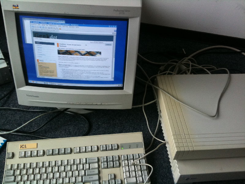
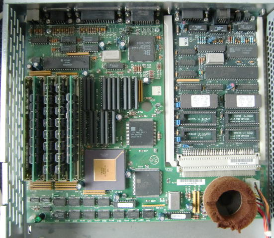
By a lucky incident I got my hands on an NCR 17c, a colo(u)r X11 Terminal featuring an 88100 @ 20MHz. All of the sudden I developed the sick ambition to run a “pure 88k X11 system”, so this NCD would be my display to start with. This is what the boring box looks from the inside:

NCD88k

After some searching I found the necessary “NCDWare” i.e. the boot-images and everything needed to get an X-Terminal running (Get it here). After some DHCP, tftp and NFS fiddling I had the latest X.org and KDE running in glorious 1280×1024 at 256 colors. But the host (In “X talk” that’s the client) was still running on an Intel x86 architecture. Yuck!

www.geekdot.com (old layout) in Konquerer running on the NCD X-Terminal:

NCD88k_KDE

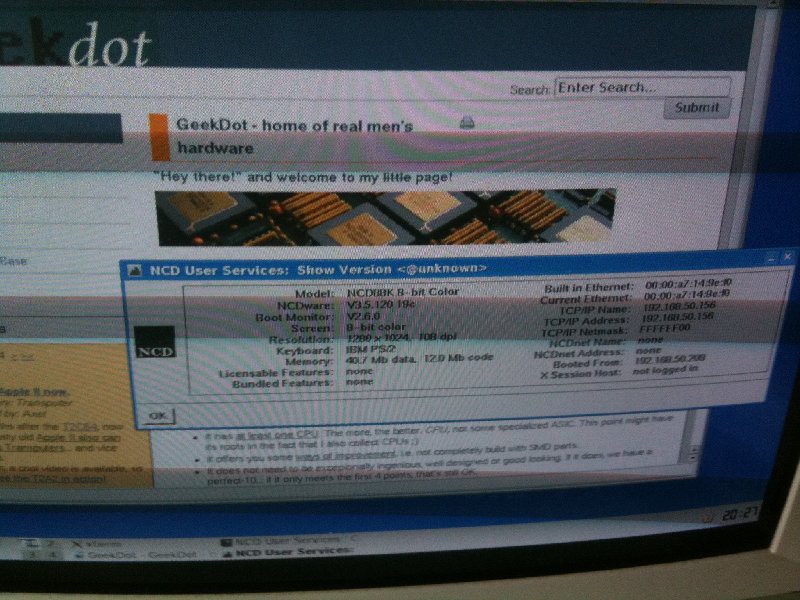
Yes, it’s the Terminal (Whopping 40MB data and 12MB code RAM):

NCD88k_screen

So out went the incredible fast MVME197LE and I compiled a rudimentary X.org on it… 2 days later that compilation was done: xdm on 88k, X11-Server on 88k. Ahhh, 88k purity 😉

Mandelbrot and Video

Like with the C64, this is probably the reason you came here:

The friggin’ fastest Mandelbrot displayed on a IIgs, ever! 😉

Yeah, you’re right, it’s not the fastest Mandelbrot calculated by an IIgs (its very own 65c816 CPU, that is)… but hey, it’s still kinda cool – and sooooo much faster!

Okey-Dokey, here we go, a complete Mandelbrot in 60s. This time in colorand zooming in! I couldn’t do that on the C64 as the C-Compiler didn’t natively support IEEE754 doubles (like Orca-C does) and having a mouse also helps a bit, too:

Wow, that was nice, wasn’t it?! (Sorry for the shaking, need to get a tripod soon)
Especially when you take in concern how ‘far’ the native 65c816 code got during the video on a ‘sped-up’ 10MHz TransWarp GS.

Like with the T2C64 version there are surely several things which could be improved, but the IIgs (even at native speed) is well capable to handle the little bit of extra work. The limiting factor is the bus-speed, i.e. how quick the Transputer can push his data into the host (IIgs). You can clearly see that by the time it took the display the 3 zooms: They all took about 60 seconds, even each zoom means more calculations as the iteration is doubled each zoom, in this case 32, 64, 128.
The Orca-C source/binary of this demo -and the previous AppleSoft sample- is available here (zip’ed PRODOS disk-image). It won’t make much sense without a T2A2 and is GS/OS-only as it uses QuickDraw II and the EventManager (for mouse & keyboard).

Final words: Don’t get too excited about the acceleration of the IIgs… it’s not accelerated at all. It’s more like a co-processor attached to it. And even then, you’ll need something really calculation-intensive to justify the time you’ll loose due to communication between the Apple and the Transputer. A single square-root for example wouldn’t make much sense.
But OTOH, that’s exactly things are handled with the Innovative Systems FPE (using a M68881). So it might be worth evaluating. Maybe I’ll write a SANE driver if I have the time to get a deeper understanding of GS/OS.

As my two targets (C64 & Apple II) are working now, I’m thinking about creating a ‘real PCB’ in the medium term. Given the rarity of the Link-Adaptor (Inmos C012) I’m currently looking into the possibility to use a larger CPLD to move the C012 into that. This would actually make this ‘project’ a product to buy.
But don’t hold your breath, need to get an eval kit first. Then some 100 days of fiddling, cursing and crying… and then more.

well, 6 years later it happened: The T2A2 became a proper PCB design… and got some additions too!

1st basic example

Like with the T2C64, the CPLD on the T2A2 maps the C012 registers into the memory area of the used slot, using just 6 addresses starting at 0xc080 + (SLOT# * 0x10). So for e.g. Slot 4 this would be:

  • BASE        (0xc080 + (4 * 0x10))  = 49344
  • Data in:    BASE                   49344
  • Data out:  (BASE + 1)           49345
  • in-status:  (BASE + 2)           49346
  • out-status:(BASE + 3)           49347
  • reset:       (BASE + 8)           49352 (writing)
  • analyse:   (BASE + 12)          49356
  • errorflag:  (BASE + 8)           49352 (reading)

With this ‘knowlege’ we can start talking to the Transputer… and to make our first babysteps we’re using BASIC. It’s pretty much the same code as used on the C64 with the exception that there’s no “elegant” timeout handling due to the missing clock in AppleSoft, so you have to wait a bit longer until you get the printout in the end.
For details about what’s going on here, see the C64 page.

 10  PRINT "INIT TRANSPUTER"
11 BASE = 49344:IN = BASE:OUT = BASE + 1:IS = BASE + 2
12 OS = BASE + 3:RESET = BASE + 8:ANA = BASE + 12
13  POKE RESET,0: POKE ANA,1: POKE RESET,1
20  REM CLEAR I/O ENABLE
21  POKE IS,0
22  POKE OS,0
30  REM READ STATI
31  PRINT "I STATUS: ";( PEEK (IS) AND 1)
35  PRINT "O STATUS: ";( PEEK (OS) AND 1)
40  PRINT "ERROR: ";( PEEK (RESET) AND 1)
45  PRINT "SENDING POKE COMMAND"
46  POKE OUT,0
50  PRINT "O STATUS: ";( PEEK (OS) AND 1)
58 :
59  PRINT "SENDING DATA TO T."
60  POKE OUT,0: POKE OUT,0: POKE OUT,0: POKE OUT,128
61  POKE OUT,12: POKE OUT,34: POKE OUT,56: POKE OUT,78
70  PRINT "I STATUS: ";( PEEK (IS) AND 1)
79 :
80  PRINT "READING FROM T."
90  POKE OUT,1: REM PEEKING
100  POKE OUT,0: POKE OUT,0: POKE OUT,0: POKE OUT,128
110  PRINT  PEEK (IN); PEEK (IN); PEEK (IN); PEEK (IN)
128  DIM R(4)
129  PRINT "SENDING PROGRAM TO TRANSPUTER..."
130  FOR X = 1 TO 24
140  READ T: POKE OUT,T
150  WAIT OS,1
160  NEXT X
170  PRINT : PRINT "READING RESULT:"
175 C = 0: REM RETRIES
180  IF C = 10 GOTO 220
181  FOR X = 0 TO 5000: NEXT X: REM DELAY
189 ER = ER + 1: IF ER = 10 GOTO 220
190  IF ( PEEK (IS) AND 1) = 0 GOTO 181
195 R(C) =  PEEK (IN)
200 C = C + 1:ER = 0
210  GOTO 180
211  REM ------------------------
220  IF C = 1 THEN  PRINT "C004 FOUND"
230  IF C = 2 THEN  PRINT "16 BIT TRANSPUTER FOUND"
240  IF C = 4 THEN  PRINT "32 BIT TRANSPUTER FOUND"
250  IF C = 0 OR C > 4 THEN  PRINT "COULD NOT IDENTIFY""
1000  DATA 23,177,209,36,242,33,252,36,242,33,248
1001  DATA 240,96,92,42,42,42,74,255,33,47,255,2,0 

Ok, if this is running fine, i.e. a Transputer was actually found and your Apple didn’t went up in smoke, we’re set for some serious numbercruncing… and a video! Yay! We love Videos, don’t we?

(I’m skipping the other sample code available on the T2C64 page. It’ll work the same on an Apple, so no need for redundancy)