All posts by Axel

http://www.geekdot.com/about-me/

Troubleshooting

This post is constantly growing, it’s mainly for me remembering not making some fu**ups again… but it might be useful for you, too 😉

Hot keys

The Helios server has quite some hotkeys you can use to navigate and control it. Per default the “hot key” is control-shift. So combining that with a 3rd key, you will get the following effect:

  • hot key ‘F1’ Switch to next window
  • hot key ‘F2’ Switch to previous window
  • hot key ‘F3’ Refresh current window
  • hot key ‘F7’ Enter built-in debugger
  • hot key ‘F8’ I/O server status request
  • hot key ‘F9’ I/O server exit
  • hot key ‘F10’ Reboot I/O server

Debugging the server

Booting Helios with server.exe you can provide a couple of debugging switches to see what’s going on:

  • A – All. Either enable all debugging, or disable any debugging which is currently active.
  • B – Boot. Give a progress report while the root processor is being booted.
  • C – Communications. Monitor transmissions to and from serial lines and similar devices.
  • D – Delete. List all files and directories being deleted.
  • E – Errors. Report any error messages generated by the I/O server.
  • F – File I/O. Give details of miscellaneous file I/O activities such as renaming files.
  • G – Graphics. Report any graphics transactions.
  • H – Raw disc. List sector reads and writes on a raw disc device.
  • I – Initialisation. Give a progress report as the I/O server initialises its various component servers.
  • J – Directory. Show details of any directory accesses.
  • K – Keyboard. Report any key presses.
  • L – Logger. Cycle the error logging destination between screen-only, file-only, and both screen and file.
  • M – Message. Report all messages sent to and from the I/O server.
  • N – Names. Show the names of objects Helios is trying to access.
  • O – Open. List all files that Helios is trying to open.
  • P – Close. Report any file close requests sent by Helios.
  • Q – Quit. Give a progress report when the I/O server tries to exit.
  • R – Read. Monitor any file reads.
  • S – Search. Report all distributed searches arriving at the I/O server.
  • T – Timeouts. Report any stream timeouts that may occur.
  • U – Nopop. In the Server windows system, toggle between pop and nopop mode.
  • V – OpenReply. Give details of replies to Open, Create, and Locate requests.
  • W – Write. Monitor any file writes.
  • X – Resources. Produce a snap shot of what the I/O server is currently doing.
  • Y – List. Give details of all debugging options.
  • Z – Reconfigure. Re-read the configuration file host.con

Those switches can be combined, e.g. server -rw

Cool: If the debug-output becomes too much to read (i.e. on screen) you can toggle the setting by pressing ctrl-shift plus the corresponding character. E.g. “c” to mute all the traffic on the serial line.

Logging

Now that we get some info about what’s going on internally, it might be a bit too much to follow on the screen (and you can’t redirect the output with “server > output.txt”). But don’t despair, there’s a way to define a logfile in HOST.CON:

logging_destination = [screen | file | both]
logfile = logbook

So simply define where you want the logging to go (screen or file or both) and define a logfile name. In this case it will be written inlogbook in the Helios root directory.
Please mind that the logfile will be overwritten (not appended) each time you reboot!

Config-Files

I cannot repeat it often enough: ALL config files (but HOST.CON) are Unix-Formatted, ie. LF instead of LF+CR. So each time something is behaving strange, check your config files for proper formatting!
I’ve spent hours of debugging just to find out I had (again) “tainted” a config file by quickly having a look with edit.exe :-/
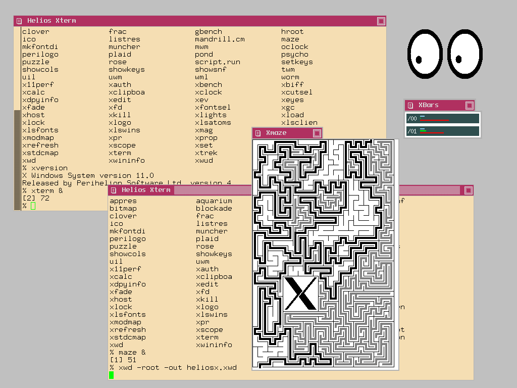
Running X Window

This is probably the pinacle of what you can do with Helios… literally, as there are probably just a handfull of people left having the needed hardware.

HELIOSX

This is because the Helios X Window System only features drivers for two “graphic cards”: The INMOS IMSB020 ISA card or the IMSB419 (or similiar) TRAM. Both sporting the INMOS G3xx framebuffer chip.

Low-level stuff

The G3xx controls the displaying device in a very low-level manner – back in those days these devices were classic cathode ray monitors and high refresh intervals guaranteed a stable, non-flickering picture (>70Hz up to 100Hz an more). Today a TFT/LCD display is the common display and those are quite picky about the refresh interval being fed into them (60-70Hz).

It might be difficult to find a TFT display which is able to “catch” the G3xx signal. But thanks (again) to Michael Brüstle, there’s a super-great tool to calculate the correct values needed to configure the G3xx to match your display… or get close to it.
You’ll need certain values for your display later in this chapter, here’s a list of them – actually that’s my setting:

screen_width = 1024
screen_height = 768
video_clock = 65 #MHz
line_time = 336
half_sync = 17
back_porch = 40
v_sync = 12
v_blank = 52
v_pre_equalise = 6
v_post_equalise = 6
transfer_delay = 21

Also, a mouse is very much needed to use X Window (surprise!). So make sure your host OS (e.g. DOS) is actually running a driver for that – I recomment CuteMouse, very small, very complete.

Because it is essential that the X server runs on the same TRAM the framebuffer/graphic controller is located. This has some influence on how to configure the system.

Using an IMSB020 aka “BOZO”

Without any TRAM installed on your BOZO, make sure to run single_user! (check /etc/nsrc)

If you’re planning to run in multiuser mode the onboard CPU must not be the root processor!
So change the links using the on-board “Linkswitch” like this:

c:\>debug.exe
o 16C 3 (i.e. set bit 0 and 1 on port 0x16C)
q

This makes the TRAM in slot 0 root processor running the network server (/00) and the onboard T805 becomes /01

Files to edit

Edit “startx” in the Helios root directory. In line 22 it reads:

  remote -d 00 run xhelios

change this to

  run -d xhelios

Now read on at “General Setup”

Using a “remote” display TRAM (like IMSB419/437/438)

Like the comment in the startx file says “If you have a multi-transputer network you must make sure that the X server is started on the processor that has the grahpics hardware.”

Files to edit

Edit “startx” in the Helios root directory. In line 22 it reads:

  remote -d 00 run xhelios

modify this to match your TRAM setup, eg. if your IMSB419 is connected to link 3 of your current (working) Transputer, it should read

  remote -d 03 run xhelios

General Setup

Check your host.con file. Around line 41 you’ll find this section:

Xsupport
mouse_resolution = 2
mouse_divisor = 2

Make sure Xsupport is uncommented. The mouse settings seemed to be fine with all my tests – you milage may vary, so play around if needed.

Copy the file
newxrc from /local/xsrc/devices to /etc
and
twmrc and/or “mwmrc” from the root folder to your home (/users/root)

Now edit newxrc to match your display values as described in the beginning of this chapter. Also check the display hardware entry in line 293 (newg332.d).
If you’re using a IMSB020, you can enable native keyboard support in line 301.
Below that are keyboard layouts (US/GB/D) and number of mouse buttons. I’m not really sure if the “processor” and “progname” values are really used – I think they’re ignored.

Feel free to edit twmrc if you like more applications to start automatically etc.

Finally, if you are running a TCP/IP network stack (i.e. tcpip and inetd are sucessfully running) you don’t have to do anything further.
If you don’t run TCP/IP you have to append “notcp” in your startx line 22, eg:

run -d xhelios notcp

You’re Done. Now start X11 calling startx from the root directory.

Going Multiuser

Yup, Helios is a Multitasking-Multiuser OS… but not quite as you might got used to it using UNIX(ish) OSes in recent times. There are some caveats:

Theory

As Helios is running on Transputers (mostly) and Transputers do not feature an MMU, there’s no ‘protected’ multitasking, i.e. a badly written application can kill (at least) the Transputer it is running on, if not the whole network. This might bring back memories of Apples System 7.x “Multi Finder” or Windoze 95 and other cooperative multitaskting solutions.
The only half-way robust way to really protect Helios processes is to ‘lock them away’ into a dedicated Transputer.

Running Multiuser (ie. providing remote login etc.) means you need at least 2 Transputers. To protect certain essential services like ‘netserver’ and ‘sessionmanager’ those have to run on the “root Transputer” (/00) which is not accessible to any user – including root. Logging in from the console on your PC will automatically put you onto the next Transputer in-line, eg. /01.
In consequence, if you like to have another user logging in over ‘telnet’ or serial console you’ll need another Transputer for that user (making it 3 in total).

Practice

So what do we need to configure to go Multiuser? First you should have your Transputer network configured and running as described 2 posts before this.
Then we check the nsrc file found in Helios’ /etc folder. Because I couldn’t say it better, I’ll copy from the Manual:
The nsrc file contains a list of options for the networking software, like the host.con
file which has a list of options for the I/O server. The nsrc file is read by the startns
program when networking software is started up, and passed in the environment to
the network server and/or Session Manager.”
(Just a refresher: network, networking and server means Transputer networks, no TCP/IP stuff and such.)

It should look somehow like this:

# root_processor = /Bozo/01
# single_user
# password_checking
# processor_protection
# no_taskforce_manager
share_root_processor
preload_netagent
waitfor_network
# 30 seconds is the default interval, -1 disables network monitoring
#monitor_interval = 10

I won’t go into every detail of each setting – there’s a Manual for that (p.58). Just make sure that ‘single_user’ is commented. For the curious amongst you: share_root_processor means the taskforce-manager, network-server and session-manager may run on the same CPU. If Helios runs in Multiuser mode like we are going to do, this is ignored anyway.

That’s it. If everything worked as described, Helios will boot all processors (but showing only /01 and /02) and logging in locally on your host machine will put you on Transputer /01. Users logging in via telnet will automatically put onto Transputer /02. This is a ps output entered in a telnet session:

% ps /00 /01 /02
Processor 00
ProcMan.0           Loader.1            netserv.4
Pipe.5              session.7           login.9
Processor 01
ProcMan.0           Loader.1            tcpip.3
inetd.4             Pipe.6              tfm.27
shell.28            telnetd.31          ttyserv.32
login.33
Processor 02
ProcMan.0           Loader.1            tfm.3
Pipe.4              shell.5             ps.7

The (inaccessible) Root-Transputer /00 is running the netserver and session-manager.
Processor /01 does the TCP/IP, inetd and telnetd handling, runs a shell (local login), cares for tty and runs a taskforce-manager (needed for parallel programs).
Finally processor /02 is the one the telnet-user actually lives and triggered the ps command from its shell.

So after all this configuring we have multiple Transputers running, TCP/IP is there and we can host multiple users (given we have enough Transputers to host them)… next and final step: X-Window!

3rd party TRAMs

Well, INMOS wasn’t the only company manufacturing TRAMs. This is a -more or less random- collection of TRAMs I was able to find in the WWW.

Because some TRAMs are of unknown origin, I’ll sort them by size…

Size-1 TRAMs

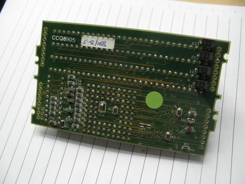
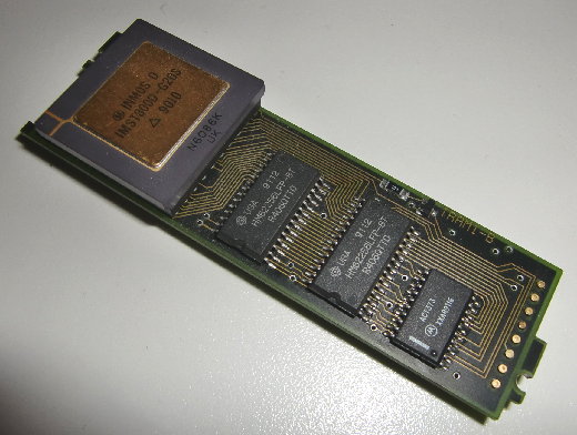
This is my 2nd smallest TRAM by RAM size. 128KB SRAM. The silk-print says “TRAM-1-B” on the front and “TRAM-1-L” on the back. I guess they’re made in Germany as it’s usual to mark the front with B (“Bauteilseite”, component-side) and L (“Lötseite”, solder-side).

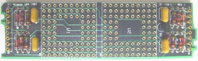
TRAM1_32k

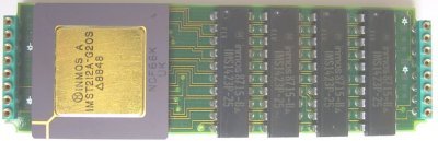
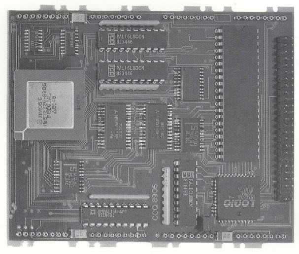
This seems to be a very early design, featureing a 16-bit T212 and some original INMOS SRAMs

Unknown_T212A_Module

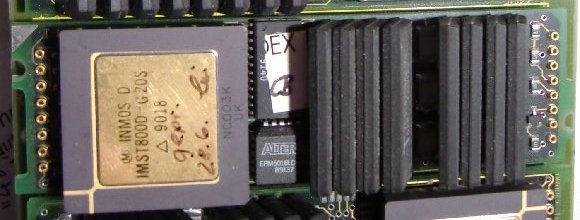
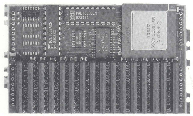
This is my “standard 1MB” TRAM. It’s labeled “ARADEX T805S“. It seems that the German ARADEX AG, originally manufacturer of cardbox packaging machines built their own TRAMs for their systems. It’s pretty highly integrated. Some but not all of them feature an ALTERA EMP5016 PLD which hold extra logic for the additionally fitted subsystem pins..

ARADEX_T805S_1M_1

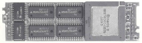
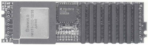
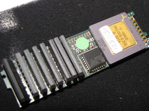
Transtech was a quite big manufacturer of all-things-Transputer. They had a big range of TRAMs in their catalogue. Pictured below are the TTM-1 (32KB SRAM), TTM-3 (1MB DRAM) and its successor TTM-7(1MB DRAM).

Transtech_TTM1

Transtech_TTM3

Transtech_TTM7

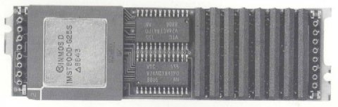
Here’s another image of which I think it’s an TTM7:

UnknownT1_1MB

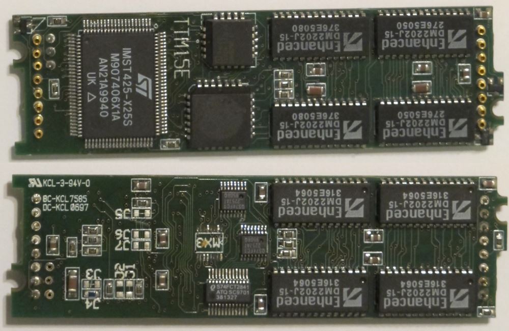
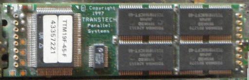
The final TRAMs of Transtech were the TTM15(e) and TTM19(f), both using the SMD package of the T800 as well as the rest of the ICs.

The TTM15E uses some interesting “Enhanced DRAM” from Enhanced Memory Systems Inc.. These include 2K SRAM in each 4Mbit DRAM chip, which increases the access speed to 12ns.
Very neat, very hard to get-by today. Restoration impossible. Mind all the jumpers on the backside – obviously a lot is configurable here.

TTM15E

The TTM19F uses what looks like modern (S)DRAM – need to evaluate that more…

TTM19F

This is a special one: Two Transputers but no RAM. It’s labeled Alcor 2T. Very nice if you need lot’s of CPU-power and can live with the 4K RAM inside the Transputer.

Alcor_2T_no_memory

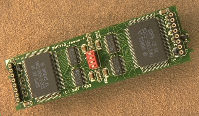
Sundance was another manufacturer concentrating on the Transputer business. They made lots of TRAMs, this SMT213 is comparable to the Alcor 2T but features two T805 Transputers in SMD as well as 1 or 4MB DRAM per Transputer (on the back) and was built in 1993 which is near the end of the Transputer era. With 4MB I’d consider this to be the “Rolls-Royce of the TRAMs”. Yummy!

Sundance SMT213

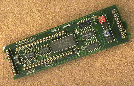
The SMT222 is an EPROM boot TRAM. You can see the socket for a 64-512KB EEPROM, inside the socket is a C011 to provide the DS-Links to the Transputer network.

Sundance SMT222

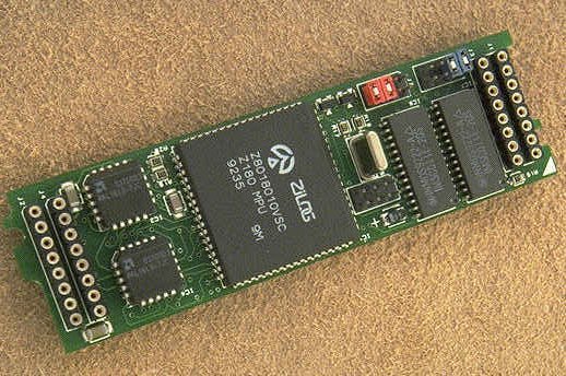
This is the SMT220, Consisting of a Z80 compatible micro controller (Z80180), a 32KByte SRAM data buffer, 512bytes of firmware and two C011 Link adapters, this TRAM is what I call an “RS232/485 interface overkill” – but I guess some industrial use required that.

Sundance_SMT220


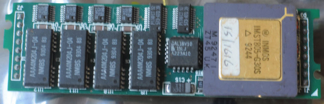
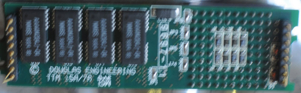
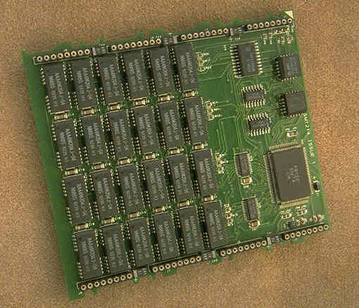
Another TRAM, using seldom used AAA4M204 SOJ DRAMs (4x1Mbit). The label says “Douglas Engineering TTM 15A/7A” (Not sure about the last number given the blurred picture I found).
This one is interesting  in so far, that it is more or less a standard SIMM-on-a-TRAM. This would make a worthwhile retro-project to recycle all those 30-pin SIMMs sleeping in our drawers 😉

DouglasEng_TTM15a_front

DouglasEng_TTM15a_back

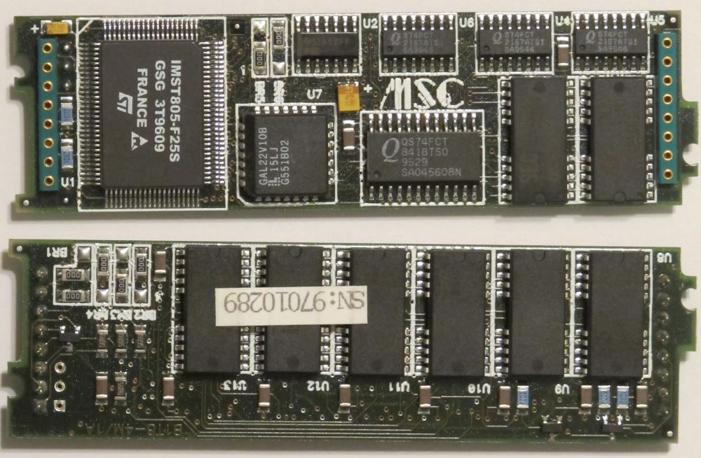
MSC (“Microcomputers Systems Components GmbH”) another pretty much unknown Transputer device manufacturer from Germany also made a SIMM-style TRAM and called it the B1T8-4M/A1.
As with the TTM15E, some settings can be configured by jumpers on the backside.

MSC-B1T8-4M_1A

Size-2 TRAMs

Next up, the STM228, a SCSI TRAM… something you want to get the most performance out of Helios or file-through-output in general.

Sundance SMT228 SCSI TRAM

The SMT229 would be the other TRAM you want for a professional system. This is the most modern ethernet controller available.

Sundance SMT229 Ethernet TRAM

The Transtech TTM-6 is a comparably boring 2MB computing TRAM. It’s an older design, like the IMS B404.

Transtech TTM6

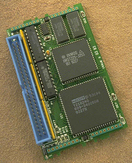
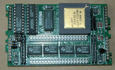
This seems to be some sort of I/O TRAM… lots of 74FCT buffers and a T225. It’s called FMX D1032.

FMXD1032

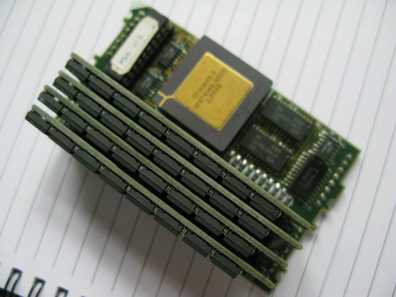
This is an interesting one: A TRAM of unknown origin using SIPPs – as memory(-expansion)!

Very cool, as you could expand its RAM up to 64MB given all addresslines are used. Downside is that this TRAM is building pretty high…

TRAM_mit_SIMM_F

and the back:

TRAM_mit_SIMM_B

Size-4 TRAMs

We’re now coming to the “Big Guns”. Starting with TTM11, another SCSI interface. It’s older than the nice SMT229, so it only has a 16-bit T222 and some old SCSI controller (my guess it’s a WD93xx chip).

Transtech TTM11

This is the Sundance SMT214, a “large memory TRAM”. It was available with 16, 24, 32 or 64MB DRAM including a T805 at 25MHz. This should be sufficient for every Transputer application… as long as nobody ports Windoze to Transputers 😉

Sundance SMT214

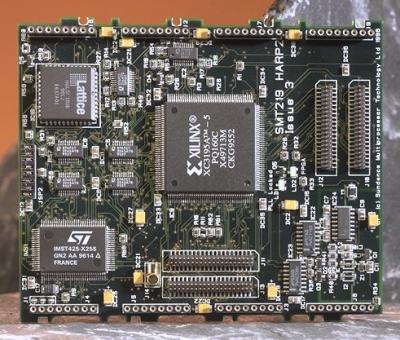
The SMT219 was the commercialized version of the HARP1 project, called HARP2 then. It’s a T425 Transputer connected to an FPGA which could be programmed for any task you needed to get done… a C64 emulator for example 😉

Sundance SMT219

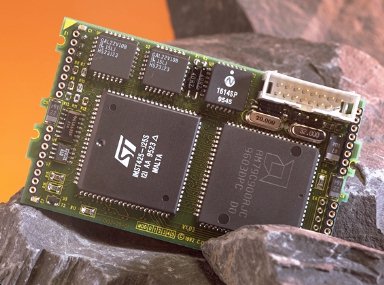
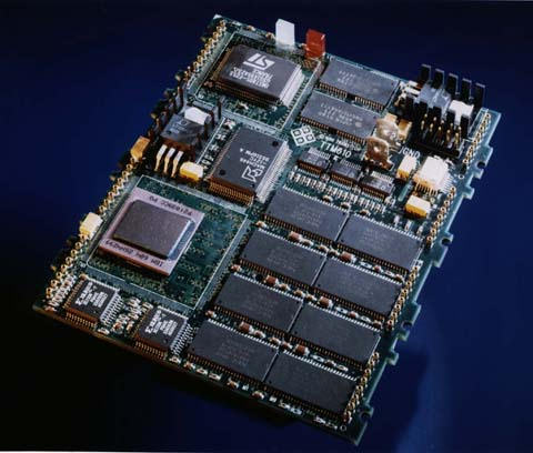
This is where it starts getting funny. Because Inmos was struggling with the next Transputer generation, other CPU manufacturers presented new quite fast  competitors, like the PowerPC from Motorola. This Transtech TTM610 featured not only a T805/25 but also a 200MHz PPC603 or 604 with 16 or 32MB of RAM.

TTM610 PowerPC TRAM

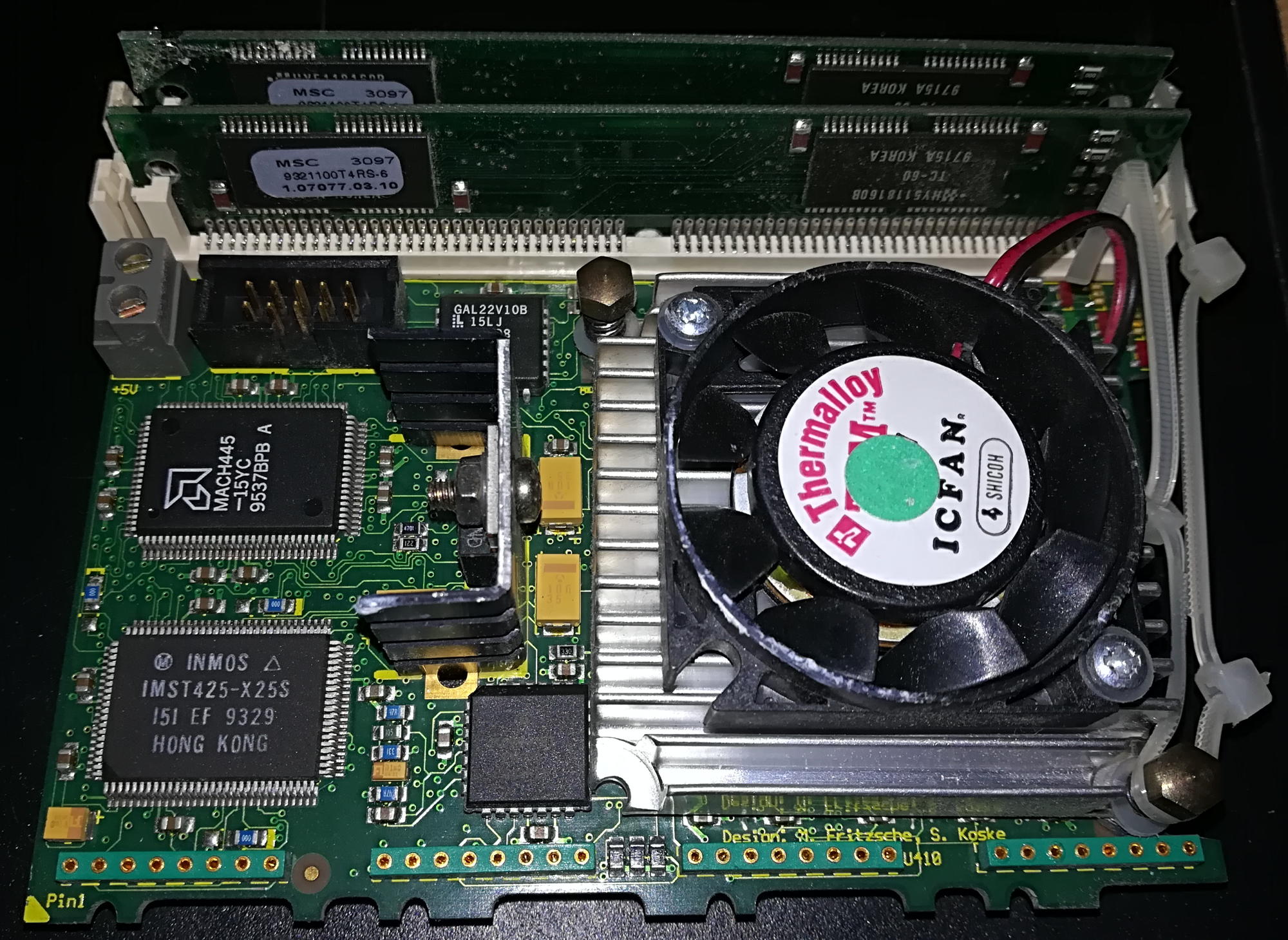
Parsytec thought the same and presented the ‘PowerTRAM’, an 80MHz PPC601 on a TRAM. Well, and there’s a T425/25, too.
If you like to know more, the Parsytec PPC systems have their own post over here.

Size-6 TRAMs

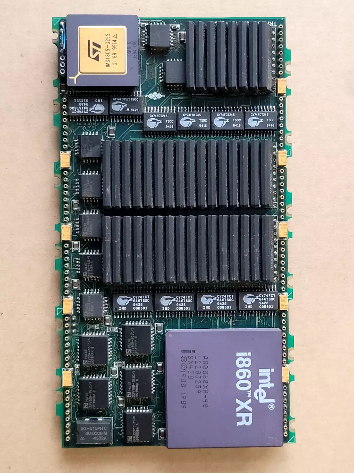
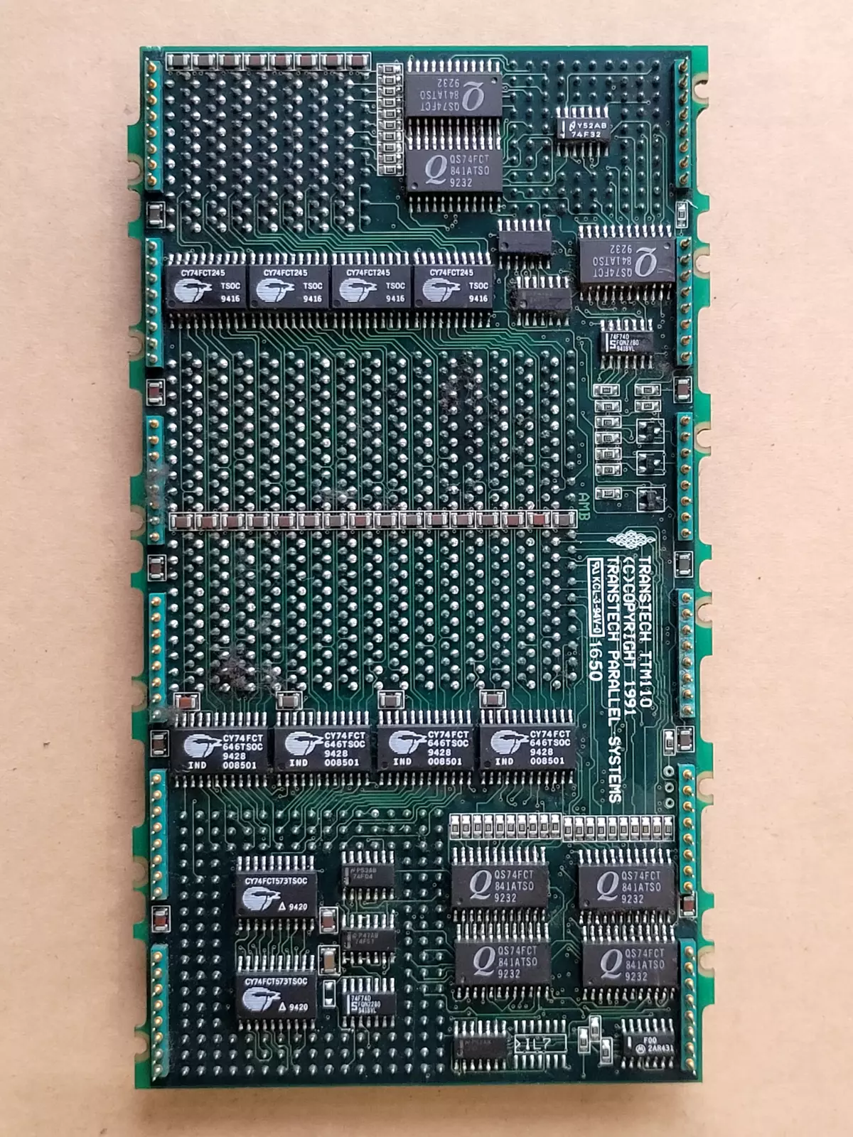
What a marriage made in hell heaven! The Transtech TTM110 joined a T805-25 (4MB)  with an Intel i860XR (16MB).
This was the ultimate powerhouse… for a short period. Until people figured out that the i860 was not the ‘Cray on a chip’ it was expected to be. Or fun to program. Or better than other CPU entering the market.

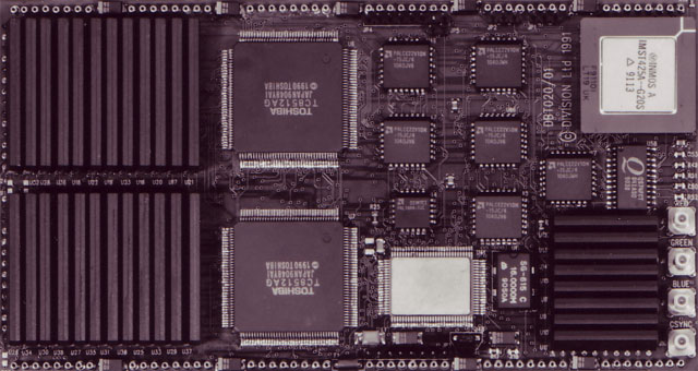
This is an graphics TRAM from “Division Ltd.” probably called DBT020/01. It features a T425 with its own 1 or 4MB RAM and 2 Toshiba TC8512 “Gouraud shading processors”, some VRAM and most likely an Inmos IMS Gxxx graphics controller.

DBT020 - unknown graphic TRAM

Size-8 TRAMs

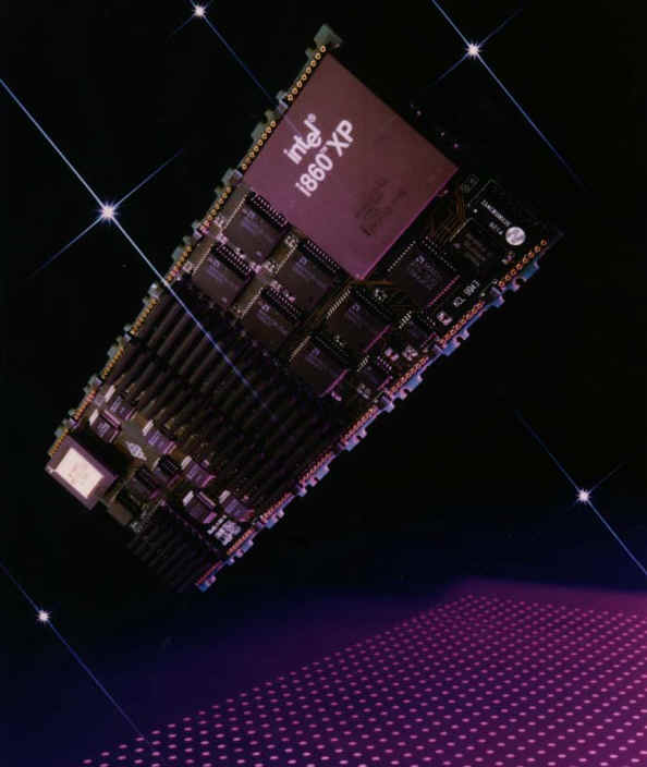
This huge beast is a TTM220 with 32 MByte DRAM coupled to both an Intel i860XP  processor, and a T805 transputer. It was the successor to the TM110.
All in all it provided the same features like the DSM860 cards (well, despite the 32bit Transputer).

TTM110 TTM220 i860 TRAM

(To be continued)

HTRAMs

As the T9000 had so many new features and architectural differences the “classic” TRAM wasn’t enough to support all that. So INMOS went to enhance the TRAM-model…

And they meant it! Instead of DIL 16 Pins of a “classic” TRAM, HTRAMs could use up to 160(!) pins to communicate to the outside world. Besides the classic 5V, also 3.3V was supplied on one pin as a tribute to the technical progress. Due to the introduction of the DS-Links (vs. OS-Links within the T4xx familiy), each of the four links of the T9000 now required 4 pins per link, resulting in 16 pins for the links alone. Plus many other special links for Events, ConfigUp/Down etc. a minimum of 60 pins were used.
Also each HTRAM now featured a PROM so it could be identified by software.

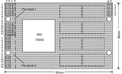
This is the pinout of an HTRAM extracted from the most recent source (SGS-Thomson B92x HTRAM datasheet, Nov. ’94)

HTRAM

Pin Row a Row b Row c Row d Row g Row h
1
2
3
4
5
ClkIn
L0SIn
L0DIn
L0DOut
L0SOut
N/C
GND
N/C
V3V3
N/C
TDI
V5V0
CupSIn
GND
CUpDIn
notTRST
L2SOut
L2DOut
L2DIn
L2SIn
EventIn0
EventIn1
EventIn2
EventIn3
EventOut0
EventOut1
EventOut2
EventOut3
9
10
11
12
13
L1SIn
L1DIn
L1DOut
L1SOut
Reset
N/C
V5V0
N/C
GND
TMS
CUpDOut
GND
CUpSOut
V3V3
TCK
L3SOut
L3DOut
L3DIn
L3SIn
V5V0
1
2
3
4
5
N/C
N/C
N/C
N/C
N/C
TDO
GND
CDnSOut
V3V3
CDnDOut
9
10
11
12
13
N/C
N/C
N/C
N/C
N/C
CDnDIn
V5V0
CDnSIn
GND
N/C

While many (i.e. 100) pins left unspecified in this pinout-map (e.g. Block 2 rows c & d, Block 3 rows e & f and the complete Block 4), they’re all used on the HTRAMs I own.
My guess is that those were used for the memory-bus, at least in the case of my Quintek board.

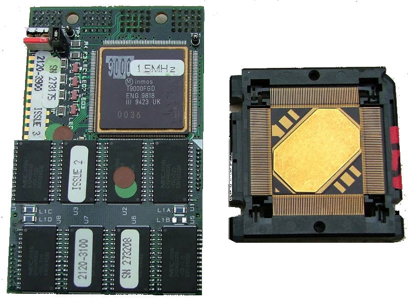
Here’s an original INMOS HTRAM, with a 15MHz T9000 engineering sample mounted, plus a T9000 (backside) next to it:

HTRAMandT9k

For a quickstart here are the 3 HTRAMs from Quintek which I own:

QT9A

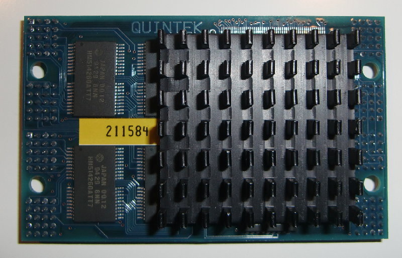
The QT9A (Rev.C in this case) is a processor HTRAM of (yet) unknown clock-speed and memory-size – I think it’s 4MB. Because the T9000 ran really hot in the prototype stage (which he never left), all of them required a compariby big heat-sink. I do not dare to remove it, given the (collector) value.

QT9A_front

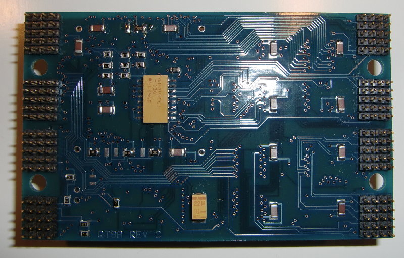
…and the backside for completeness 😉

QT9A_back

QT9H

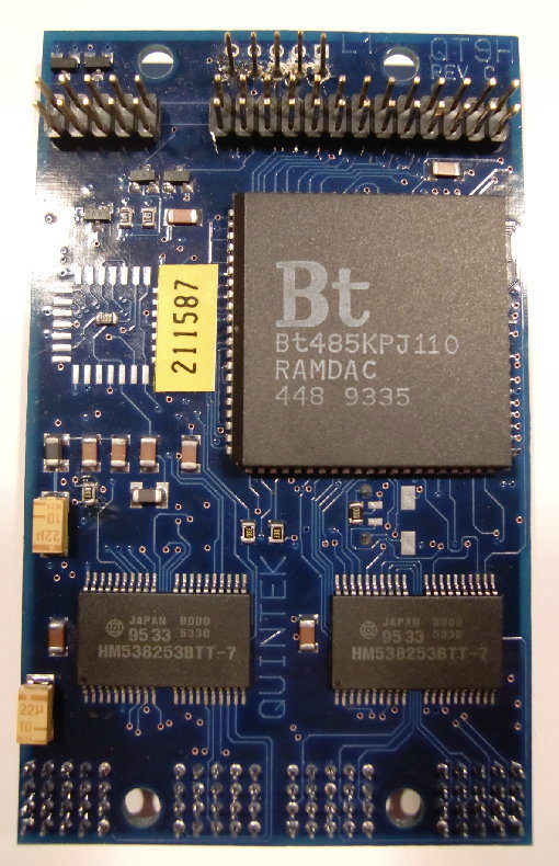
This is a display HTRAM featureing a Bt485 RAMDAC, 2MB VRAM but no video-output part. The video signal is delivered to a pin-row which is going connected to a VGA-featurebus on a graphics card. It’s a Rev.C part, like the QT9A.

This and the following HTRAM were fitted into Slots 5 and 5 on the HTRAM-board which are quite special slots: They don’t offer the pin-blocks 1 & 2, i.e. no DS-Links etc.! That said they do feature fully populated pin-blocks 3 & 4 which underlines my assumption that those pins are meant for direct memory-mapping.
In the case of a Video & Encoding HTRAM this makes totally sense because it gives the Transputer even faster access to the Video-RAM than pumping all the data over the Links.
Which leaves yet-another-riddle-to-be-solved: Where are those HTRAM mapped into the T9000s memory?

QT9H_front

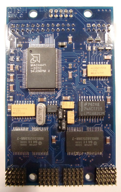
…quite a lot is happening on the back-side, too:

QT9H_back

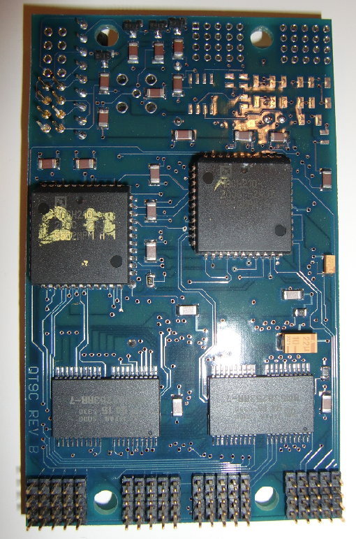
QT9C

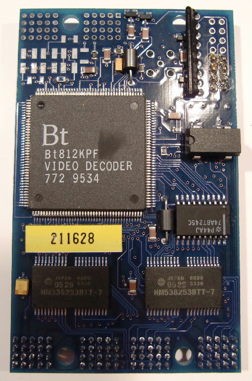
A video digitizing HTRAM using the BrookTree/Conexant Bt812 chip and having 2MB VRAM, too… this time “Rev.B”.

QT9C_front

and the back side…

QT9C_back

To be continued…

Putting the DSM to use

So after the lengthy description of the DSM cards – how can we make use of them? As said in the previous chapter, they were shipped with an assembler and even an early version of GCC (1.3) so development is pretty straightforward.

Activation

First, you have to understand how the cards integrate themselves into an ISA/EISA system. While the three versions (8, 16, 32bit) differ in some areas, the integration is more or less similar:

Each version offers a latch for controlling the card. This means to activate the card by writing bits to that latch to define a memory-window inside the hosts RAM to blend-in the cards dual-ported RAM  and/or resetting it etc.. The latch is accessible through an IO-port set by jumpers on the card (default 0x300).

So for the ISA cards you have to for example write a 0xC2 at that port-adress to reset & activate the card and use the mem-window of 0xDC000-DC7FF. In Turbo-Pascal this would be something like:

port[$300] := $c2;

This gives you a 2K mem-window to exchange data between the DSM and the host (just 1K for the DSM860-8).

The EISA cards obviously use other ports depending on the slot-number, so this would be an example to do the same for am DSM860-32, this time in Turbo-C:

outportb(slot_no * 0x1000 + 0x800, 0xc2); // For slot #2 this would be 0x2800
This would also open a mem-window at 0xDC000, this time up to 0xDCFFF, i.e. 4K long.

Memory

As mentioned above, the Host and the DSM-card are communicating through a memory-window of diffenrent sizes, depending on the DSM used. Due to their nature, the memory is looking different though. That said, at least they’re both litte-endian, so no byte-swapping needed.

The 80×86 side

For the hosting PC, memory looks pretty straightforward. 1KB-4KB of RAM somewhere in ‘lower-RAM’, that’s it.
While we don’t use it, it’s worth mentioning that there’s a 2nd memory window called “Common“. This is fixed at a specific address and is shared between all possible cards plugged into one host. I guess you already got it: This enables easy multi-processor communication… and gives a lot of possibilities for f**k-ups.

The i860 side

The memory-mapping on the i860-side is the same for the 16 and 32bit cards, the dual-ported RAM is located at 0xd0040000 (0xC0000000 for the DSM-8).
In any case the i860 memory is linear, 64bit wide and always on a 64-bit boundary. This means you have to read the DP-RAM area differently depending on which card you run your code. Here’s an example of how the DP-RAM looks like on the Host- and i860 side:

Host DP-RAM in DOS ‘debug’
-d dc00:0000
DC00:0000 11 22 33 44 55 66 77 88 ...

which would look like this on the i860 side:

DSM/8
C0000000 - 11 xx xx xx xx xx xx xx 22 xx xx xx xx xx xx xx
C0000010 - 33 xx xx xx xx xx xx xx 44 xx xx xx xx xx xx xx
C0000020 - 55 xx xx xx xx xx xx xx 66 xx xx xx xx xx xx xx
C0000030 - 77 xx xx xx xx xx xx xx 88 xx xx xx xx xx xx xx

DSM/16
D0040000 - 11 22 xx xx xx xx xx xx 33 44 xx xx xx xx xx xx
D0040010 - 55 66 xx xx xx xx xx xx 77 88 xx xx xx xx xx xx

DSM/32
D0040000 - 11 22 33 44 xx xx xx xx 55 66 77 88 xx xx xx xx

So reading and writing from/to the DP-RAM involves some thinking to be done by the programmer. Here are two code-snippets showing the difference between reading the DP-RAM on a DSM860-8 and an DSM860-16. First the ‘8 bit version’:

mov 4*8,r4
readloop:
ld.b 0(r15),r14  // Load BYTE from DP-RAM
st.b r14,0(r29)  // store it destination
addu 8,r15,r15   // add 8 to read-mem-pointer
addu 1,r29,r29   // add 1 to desitination-mem-pointer
addu -1,r4,r4    // loop-counter
xor r0,r4,r0     // Test Zero
bnc readloop

And the same for the DSM860-16:

mov 2*8,r4
readloop:
ld.s 0(r15),r14  // Load SHORT (2 Bytes) from DP-RAM
st.s r14,0(r29)  // store it destination
addu 8,r15,r15   // add 8 to read-mem-pointer
addu 2,r29,r29   // add 2(!) to desitination-mem-pointer  (short <> byte)
addu -1,r4,r4    // loop-counter
xor r0,r4,r0     // Test Zero
bnc readloop

Because of reading SHORTs (ld.s) the DSM860-16 version has to loop just 16 times while the 8-bit version has to do that 32 times.
Same applies to writing. You will find an example in the Mandelbrot program (Commented source file).

[This is work-in-progress and will expanded over time]

Action!

So here we go, finally some program running showing all the power behind the i860. I took the Mandelbrot example from R.D.Klein and modified it a bit, well quite a bit as it was written for the DSM860-8 and provided CGA output (yuck!).

Like most “external accelerator” programs, there’s one part running on the accelerator (the i860 in this case) and one part running on the host doing useful things with the provided data. In this case we have an i860 assembler code doing the number-crunching on the Mandelbrot algorithm using the i860’s ability of ‘dual instruction-mode‘ and some code done in Trubo-Pascal handling the display and zooming.
The latter was extended to use SVGA (640x480x256) output and providing an interrupt driven timer. [sourcecode package cleanup is still work in progress]

Here are the two running full steam ahead:

Some things worth to mention:

  • The host being used here is a P1 133MHz, a bit unfair comparing that to a 40MHz i860 – OTOH they seem quite comparable when it comes down to Mandelbrot crunching speed.
  • To calculate the Mandelbrot the same speed as it took the Pentium (~15s) I needed five T800-20 according to my benchmarks.
  • To even achieve the 8.2s of the i860 I had to run 9(!) T800-20 in parallel.
  • A i486DX/33 took 66 sec to do the same (8.25 times slower!), while it still took 34s for a i486DX2/66!

So while all that moaning about the bad ‘programmability’ and slow context-changes of the i860 are completely correct, in certain tasks that CPU was indeed a real screamer!

GigaCluster

The GC system (GigaCluster) was Parsytecs entry into the Supercomputing world aiming the TOP500 list.
Actually there were two models available. The pure Transputer model was called “GCel” (GigaCluster entry level) while its successor using Motorolas PPC601 CPUs was simply called “GC”. The different sources in the Web are mixing those two model-names at random – I’m sticking to GC throughout this article, even it’s the Transputer model.

Architecture

A GC machine is built up from a number of GigaCubes. Each GigaCube represents a self-contained unit/case with its own power supply, I/O channels and interconnection to other GigaCubes. Each GigaCube contains 64 T805 processors packaged at high-density.
A GigaCube was available as a stand-alone machine, called the GC-1/64 (Peak performance = 12.8 GIPS (32-bit), 1.6 GFLOPS (64-bit))
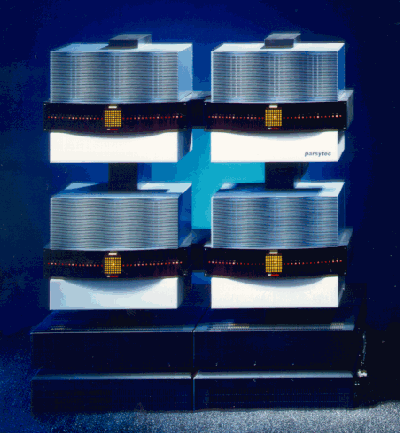
This is a picture of 4 GigaCubes (GC-2, i.e. 256 Transputers)

GigaCubeCases

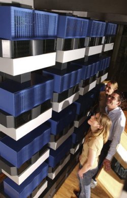
 This picture shows the biggest ever built GC. It’s the GC-3 (1024 CPUs) delivered to the university of Paderborn (Germany) which is now on display stored away somewhere in the Heinrich-Nixdorf Computer Museum in the same city (Thanks to Abraham V. giving me the update that they removed it from public display. Shame on them! – been there myself in 2018 and yes, it’s still not on display):

GC_paderborn

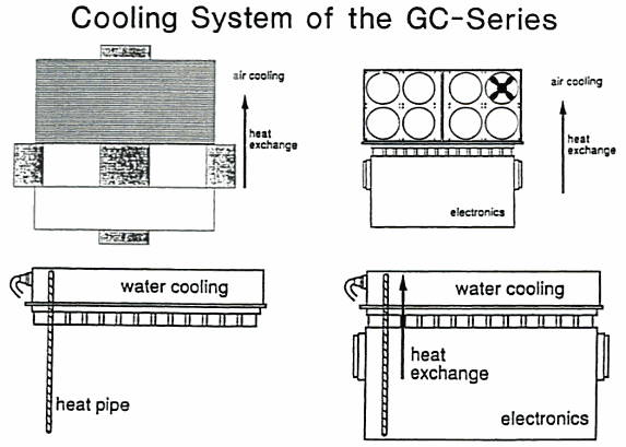
Machines larger than the GC-3 (>= 1024 processors) would have required water cooling which is facilitated by the use of “heat pipes”. Here’s a sketch I’ve found showing where the cooling was located in the GigaCube housing.

GC-Cooling

How did Parsytec connect those heat-pipes with the board? By a lucky incident a nice guy provided me with new, detailed photos describing how cooling was managed.

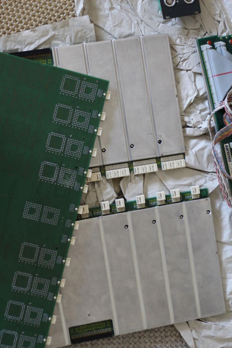
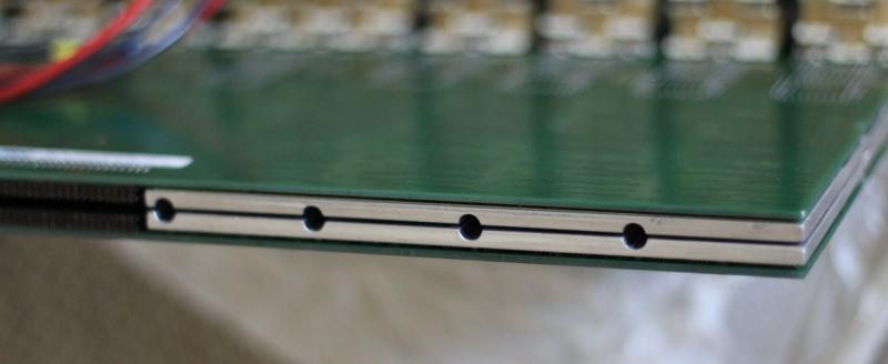
Contrary to a “normal” GigaCluster CPU board (or cluster, as described further down), CPU boards in GC-3 were covered by a massive aluminum heat-spreader, featuring “half-pipes” milled into the aluminum as shown in this picture:

GC_CPUboards

When put back-to-back into the Backplane, those half-pipes created a full pipe into which the heat-pipe was “sunk”. Very clever, indeed.

GC_CPUboardsPipes

Fun-findings: If a GC-4 whould have ever been built, it would have looked like this rendering (bear in mind: 4096 Transputers!)

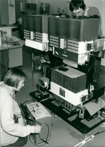
And here’s a nice press-photograph showing Angela Merkel building a GC… naah, just kidding:

Node

A GigaCube consists of four clusters of 16 processors and has self-contained redundancy, control processor, power supply and cooling.
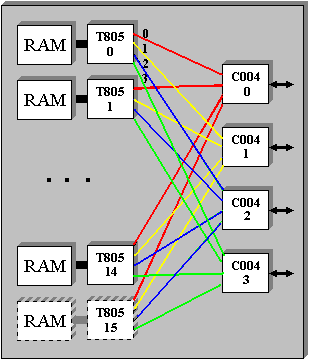
A cluster is the basic architectural unit and consists of 16 Inmos IMS T805 transputers running at 30MHz, the EDC-protected memories (up to 4Mbytes per T805), a further redundant T805, the local link connections and 4 Inmos C004 routing chips. Each link of the T805 is connected to a different C004, thus making it hardware fault tolerant. Redundancy in a cluster ensures overall probability of failure is less than that of a single typical chip.
This is a diagramm of how a cluster was connected internally:

cluster

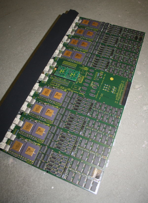
And this is a photogaph of a cluster as it was used in the Parsytec x’plorer. Besides the missing C004s it is identical to the those used in the CG:

FullBoard

I/O

Inside a GigaCube each processor cluster has eight dedicated links with a bidirectional bandwidth of 20 Mbytes/s. Each of the two sets of 16 links with an additional control link forms a basic I/O channel. These are logically driven by the control processor and therefore allow it to control the attached devices if required. For the largest systems shared I/O devices amongst the GigaCubes is achieved with a special module (IONM) which may be cascaded.

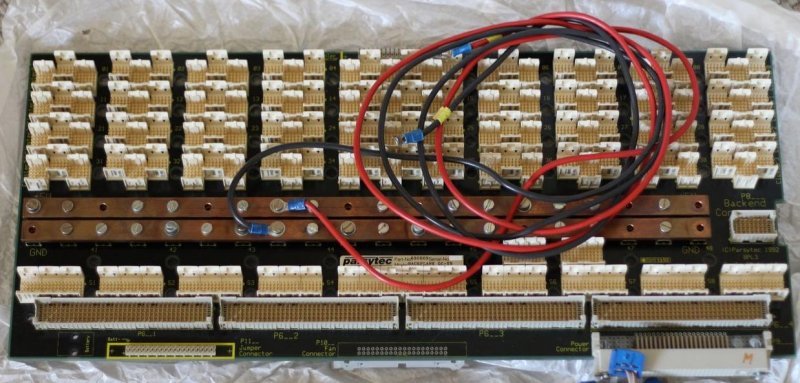
Up to 4 clusters were plugged into a Backplane which looks like this:

GC_Backplane_1

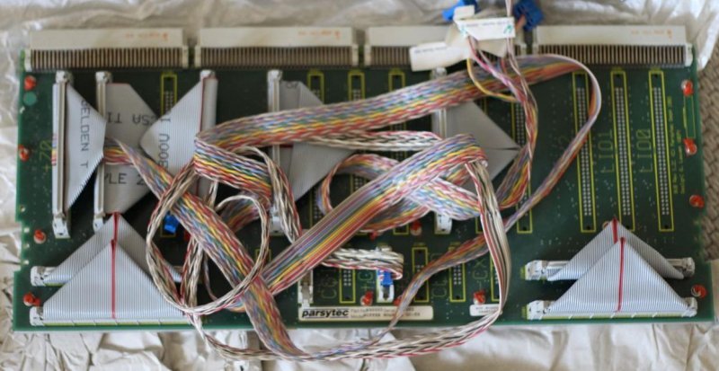
Next to the four cluster-boards, a buffer-board was seated handling the communication “outside of the cube”:

GC_Bufferboard_1

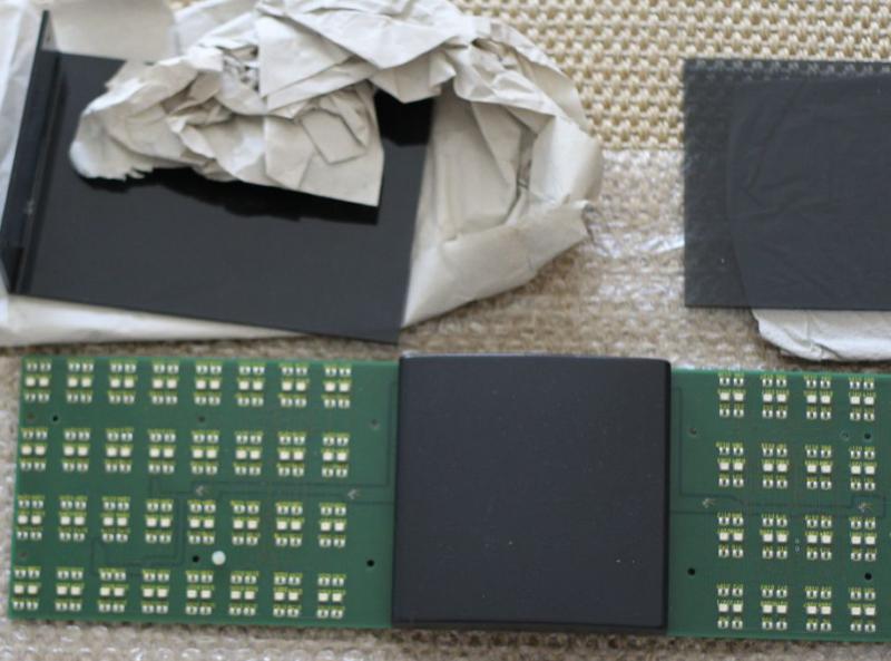
As you most certainly know, Blinkenlights is an absolute must-have (and the 6th commandment in Axels laws ;)), so each Cube had its own LED panel – 128 LEDs, 2 for each Transputer in the Cluster – hidden behind a sleek acrylic glass:

GC_LEDpanel

Topology

The communications structure of the machine is software configurable. Each T805 has four hard links and up to 16384 virtual links. Each hard link is connected to a C004 32×32 way cross-bar switch. The C004 can determine the destination of a message and switch automatically with extremely low latency.

Operating System

Ofically the CG-machines were meant to be used with PARIX. PARIX is based on UNIX with parallel extensions, supports Remote Procedure Call and the I/O library is a subset of the POSIX standard.
Being a “good Transputer system” the GCs can also run Helios. Helios is supporting the special reset-mechanism of Parsytec out of the box.

Parsytec was involved in the first phase of the GPMIMD project. However, disagreement with the other members, Meiko, Parsys, Inmos and Telmat, on the adoption of a single physical architecture, prompted them to announce their own T9000 machine, based on the design of the CG machines. Due to INMOS’ problems with the T9000, Parsytec switched to the Motorola 604 PowerPC CPUs. This led to their “hybrid” systems degrading Transputers as communication processors and having the PPCs doing the computational work.
While I cannot support that policy, here’s a separate Post about those bastard machines due to frequent requests 😉