Tag Archives: i860

DSM Software

I’m in the lucky position to own the last offically released software package for the DSM860 cards.
That said, it’s a mishmash of different tools, code and compilers not always compatible with the different boards (860/8, 860/16 and 860/32). Still the sources and specifically the assembler and C compiler may be helpful for a kickstart.
I’ve adjusted the installer to create a single-install instead of the original 3 floppies installation. See the readme.txt file for more details.

Download it here.

And if you’re interested, here is the the source & binaries for my Mandelbrot example.

Kerberos

Kerberos is the machine I’ve specifically built for hosting all 3 DSM860 cards I own.
The name was chosen because the hell-hound Kerberos (Latin ‘Cerberus’, Greek ‘Κέρβερος’) is mostly depicted with three heads and the Greek myths offer innumerable possibilities for a nice g[r]eek name space 😉

The quest for the right motherboard was not easy. It should be small, still featuring as many EISA slots as possible. In the end it became a Gigabyte GA-486SA having some quite unique features for its time:

  • 8 EISA slots
  • 2 of them also having Vesa-Local-Bus connectors
  • A Weitek 4167 Socket
  • 8 SIMM slots

Because it was clear I will use-up 6 slots just for the 3 DSM860 cards (being sandwiched boards) I wanted to fill the remaining 2 slots as clever as possible.
After another year (!) of searching I was able to get my greedy little hands onto a Western Digital ‘Ports’o’Call‘ Vesa-Local card. This is a rare do-it-all card saving lots of slots, specifically:

  • WD90c33 VGA (1-2MB) connected to the VL-Bus (fast!)
  • Appian Local Bus IDE controller (also quite fast)
  • Floppy controller
  • 2S/1P peripheral controller

In a sentence: Everything a basic system needs to work! The remaining slot was planned for a NIC making the system complete.
Because I was expecting quite some heat coming from the three i860 I’ve opted for a desktop case so that the heat can easily dissipate through the open casing – also I was prepared for lots of plugging and unplugging of cards, jumpers etc. which is much easier with a desktop case.

Golden Rule #1 of hardware fiddling: One step after the other!

So before filling the system up to its rim, I started with just one DSM860. It quickly became clear that there was no way in using the ports’o’call’s WD90c31 as the server running on the DSMs does only support certain VGA cards (if you like to have graphic output), namely some very obsolete, non-standard Genoa cards…and in its latest version: Good old ET4000!

So the nice ports’o’call had to make place for a standard multi-IO controller and the 2nd slot was used for an ET4000. That setup worked quite nicely!
After the last DSM860/32 board was fixed, I was ready to “stuff that turkey”.

One card after the other went into the slots – that’s what I call a crowded house:

Animation1

As the animation above is not the highest quality (file size!), here are some more shots…

All seats taken, sorry:

fullhouse

The money-shot 😉 Indeed… in 1991 you would have payed 48.000 German Marks (~US$ 24k) for the DSM860’s alone… plus a 486DX/2 system with a whopping 32MB of RAM (~9500 Marks = ~US$ 4750). So that’s a total of $US 28.750 or the average income/year (1991) in the US.

moneyshot

Finally some of Kerberos facts:

  • 3 x i860/40MHz each 8MB RAM (= 180-240 ‘marketing-MFLOPS’ / 360 ‘marketing-MIPS’)
  • Handcoded code using LINDA SMP techniques can realistically reach ~80 MFLOPS on this system, that’s about the speed of a Cray-1 or … a Pentium Pro 200 :-/
  • 1 x 486/DX2-66, 32 MB RAM (~3.5 MFLOPS)
  • Complete system (w/o display) draws 140W when running full steam ahead. Which is about the same a recent (’09) Intel Core2/Core i7 or AMD Phenom needs @ 3.2GHz – just the CPU though!

Kontron SBC860

First of all: I do not own this card, I just list it for completeness.
Everything written here is accumulated through computer magazine articles or internet sources – if you know more or better, I’m always happy to hear from you.

This is a picture of the Kontron SBC860 (courtesy of Jörg Heilmann):

Kontron_SBC8601

As you can see the SBC860 is much higher integrated as all other i860 cards presented on this page (while it bears quite some similarities with the rev.1.6 of the DSM860-OEM/16), most parts being used in modern SMD form.
It’s a single, full-length 16-bit ISA card, featuring 8 proprietary SIMM slots for up to 32MB RAM.

As far as I can see, the SBC860 has its own bus-interface so no fancy Transputer-Links or such.
In the upper right corner of the card are two huge “pin arrays” (each with 112 pins), the left one having two blue jumpers set. Iassume this could be some sort of expansion-bus for add-ons. Interesting fact: Exactly this part was missing on the board which was reviewed in the German magazine c’t 91/3. As Jörgs card says “R14/A” on one label this might hint towards his card being a later, updated version.

The price of the card was as hefty as their competitors: 33 MHz/8 MByte 13212 DM, 40 MHz/32 MByte at ~21200 DM in the year 1991 (US$ was roughly half)

P3 = Interrupt Vector
7  10  11  12
:   :   :   :

P4 = I/O Base Address   8 consecutive Port Adresses, between 0x100 and 0x3F8

   P4              I/O Addr
==============================
::IIIII            0x300
::II:II :::        0x320
::IIII: :::        0x308
:I::III            0x200 

The SPEA cards

Between 1990 and 1995 the German multimedia-card manufacturer SPEA was one of the leading companies in this sector (When ATI was comparably small and NVIDIA not even founded).
They offered a wide range of display-cards, from a simple ET4000 up to very expensive CAD/CAM cards using various graphic chips like the TIGA controllers, Hitachi ACRTC, Weitek, S3, 3DLabs and… of course the i860.
Later SPEA was bought by Diamond Multimedia and some employees started their own company to finalize the graphic chip they already started to design when being with SPEA (read more here… article in German, sorry).

Two SPEA cards using the i860 were built. The first was the

SPEA Fire

SPEA-Fire

This full-size ISA card features a 33MHz i860 with 4MB own RAM as well as 2MB VRAM. An Inmos G364 graphics controller is in charge for creating a picture on the monitor – BTW that’s the last and fastest graphics controller which was manufactured by Inmos.
Theoretically, this card could be called an INMOS B020 on steroids.

As this is “just” a 3D subsystem, a standard VGA was still needed for all 2D stuff. Its video signal was then looped-through the SPEA Fire… just like the Voodoo cards did it some years later.

A recent photo I’ve found on ePay shows, that there was a proprietary memory expansion available, which has to be plugged next to the i860. Probably expanding the RAM to 8MB, which can be considered as an quite serious amount of RAM back in those days.

SPEAFire_RAM_upgrade

Interestingly the manual briefly touches the possibility to be programmed with own applications using Intels APX system. Sad enough, the APX is not included on the driver disks and was sold separately for a lot of money.

FGA860

SPEA-FGA860

The FGA860 is the bigger brother of the SPEA Fire. Actually it’s two boards sandwiched together: The one on top is -again- called the Fire-Board. But this time it is designed completely different. There is no RAMDAC or such… just the i860, RAM (16MB) and some custom- and bus-logic.
Behind this, there’s a full-blown TIGA card called FGA-4E, using a TMS34020/32Mhz with 4MB DRAM and 2MB VRAM. Not so usual is the also included VGA part on the FGA-4E. This way you can save an ISA slot for the needed VGA card.

The Fire-Board was available for 5700 German Marks, the FGA-4E added another hefty 10.820 Marks making a total of 16.520 Marks (1990/91 that was about US$ 8000)!
But for that money you got a “graphic subsystem” which was capable of 300.000 2-D vectors/s (10 Pixel long) and amazing 30.000 gouraud-shaded polygons/s (10 × 10 Pixels).
[Back then, that really was amazing… today every mobile phone might be better in 3D. Here are some numbers for comparison/amusement:
3DLabs GLINT 300SX: 500.000/300.000]

Here’s a view from the top… not really much to see. It’s very hard to pry those cards from each other. I guess, they were never intended to be separated again.

SPEA-FGA860_sandwich

If you are in need of the drivers, I make them available here. It’s the IMHO most recent version from August 1994 including an AutoCAD 13 driver update.

Hauppauge 4860

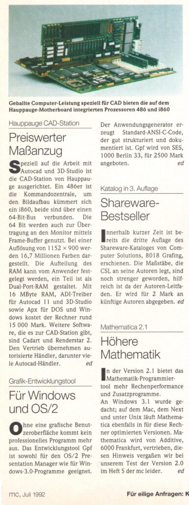
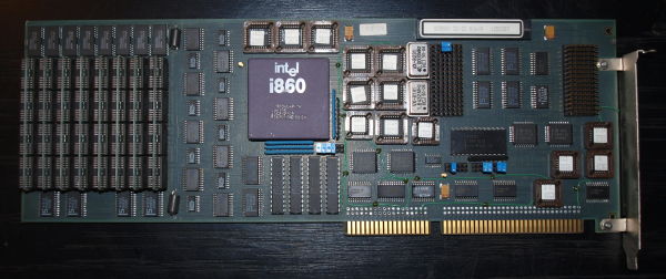
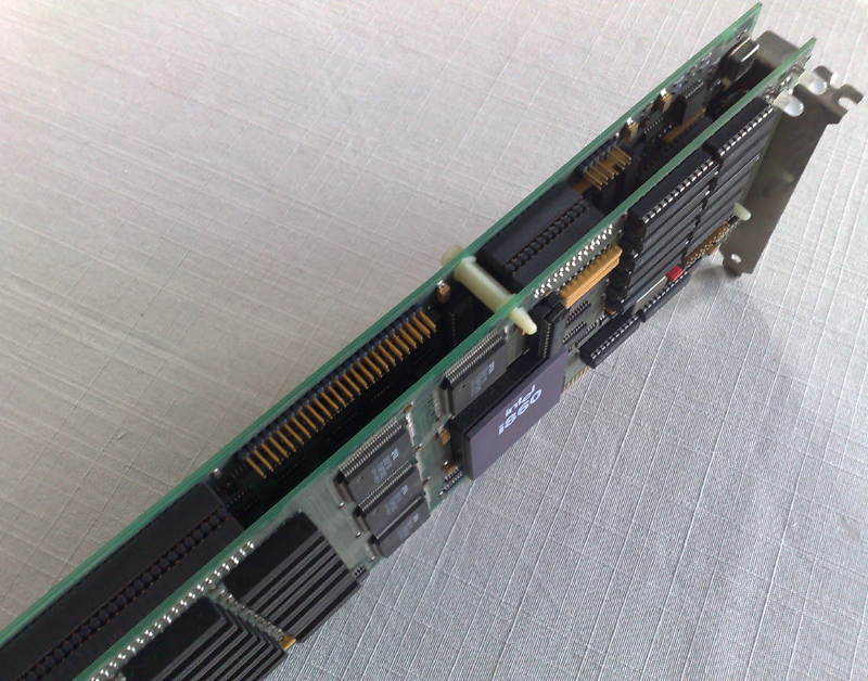
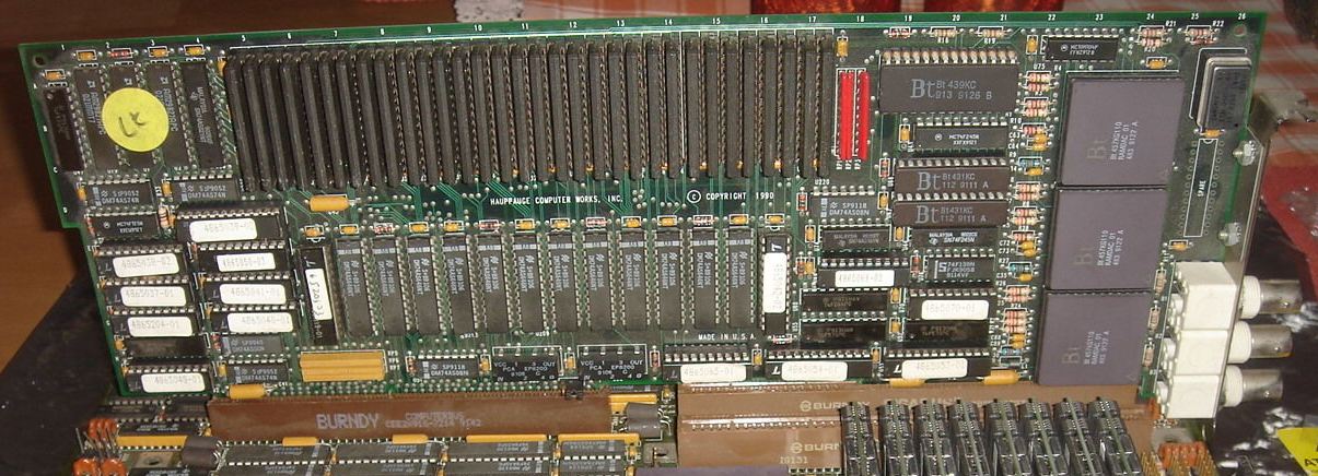
Not really an expansion card but a full blown EISA motherboard featuring an i80486 and an i80860 socket directly on board – thus the ingenious name Hauppauge 4860. The i860 can work in parallel to the i486, both sharing the on-board RAM which can be freely partitioned. But theoretically the i860 could also run completely alone… at least Hauppauge mentions this in the manual, announcing a UNIX version for this option (of course that never shipped).

This board is quite a huge beast, full size AT that is. For its time it was regarded as high-quality but besides 1 ASIC and 2 Intel chip set ICs there are a lot of logic ICs and PALs.
I’d say it’s a ‘IC graveyard’ and one of the most exciting 80486 boards ever made.
(And a real diva when it comes to add cards :-/ More on this further down)

FullBoard

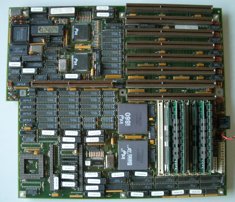
These are the main specs:

  • 80486 socket (does not run stable with DX/2), 25 or 33MHz
  • 80860 socket (same clock speed as 486)
  • Weitek 4167 (aka Abacus) mem-mapped FPU socket
  • Intel “485TurboCache Module” socket
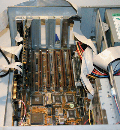
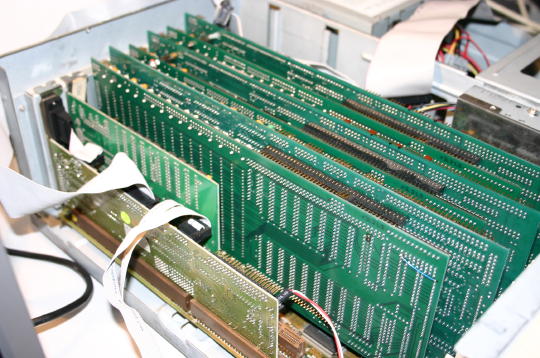
  • 7-8 EISA Slots (depending on revision)
  • Intel EISA chip set consisting of 82358-33 EISA Bus Controller and 82357 Integrated System Peripheral
  • On-board Serial/Parallel and PS/2 mouse support
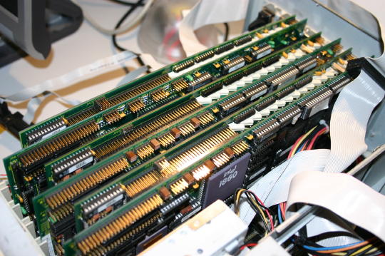
  • 8 SIMM sockets for up to 64MB (Fast Page Mode,parity – No chance with EDO or non-parity)
  • Award “486 Modular BIOS v4.10” / BIOS level 1.01 -obviously specifically tailored to the 486/860 needs.

Because there are so many things on this manly mainboard, I will go into further detail based on quadrants:

Lower right

LowerRight

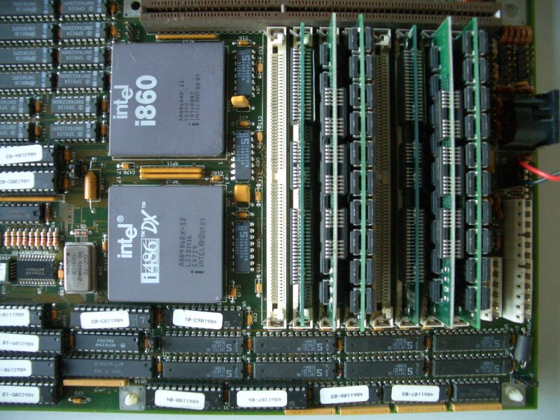
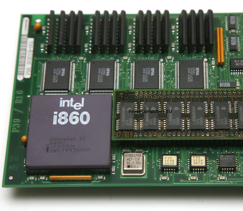
Well, that’s where all the mojo sits, right. The two processors side by side – ahhh – what a macho view! 😉 Mind the single oscillator: This means both CPUs run at the same speed, which is a bit of a pity, as the i860 was/is available at clock speeds up to 40MHz. Because Intel never really crossed the 33MHz external clock (the 50MHz 486 was quickly replaced by clock doubling versions due to heat issues) for their 486 processor, this is the highest common denominator.
That said, the Hauppauge 4860 does not support DX/2 processors… believe me I tried them all (even up to 5×86 w/ voltage regulator).Yes, it’s running fine one day while failing to boot the next day. So be sporting about it, an AMD 5×86/133 will easily outperform the i860/33 and who would like to put him ashame like this?

Ok, next to the two brains you can easily spot the 8 SIMM slots. It’s not easy to satisfy the RAM specs here: PS/2 SIMMs, optimally 60ns, Fast Page Mode (FPM) with parity – only up to 8MB per SIMM will be addressed. I had to learn that it is not so easy anymore to find those SIMMs today :-/
At the rightmost edge of the board you can see the classic AT-style power connectors… with an additional connector for 5V. Yup, it’s a server board, having all RAM- & EISA-slots populated, this beast can slurp quite some juice. Ok, it still would be nothing compared to todays insane 1000W power supplies feeding quad-core CPUs and dual graphic-cards.

At the lower edge you can spot quite some logic ICs. That’s a part of the memory interface – yeah, no stinkin’ ASIC, just TTL logic and many GALs.
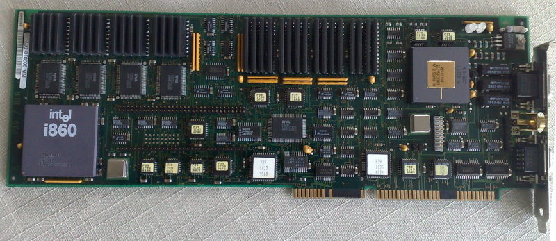
Lower left

LowerLeft

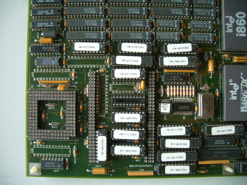
While or two processors still peeking over the right edge, you can easily spot even 2 more sockets on this board. The square one on the left is meant for a Weitek 4167 (also known as  “Abacus”) while the two pin-rows in the middle of the picture are planned for an “Intel 485TurboCache” (yes, that’s 485) module.
Honestly, I have no idea why Hauppauge added the Weitek 4167. As it was just about a bit faster than the inbuilt FPU of the 486/33 (~10% overall), it had no chance against the i860 – both needed programs which were specifically made for them, so compatibility wasn’t an argument for both. I guess it was added on the board just because they could… which is the right spirit!
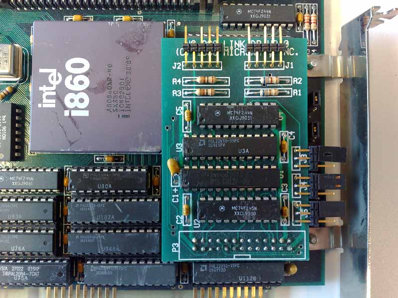
The socket for the “485 TurboCache” was a good idea – which seems to went wrong in the case of this board. The module generally is nothing more than an i82485 cache controller with 64 or 128k SRAM. After years of searching I found two different models, both not working with the 4860. This seems to be a known issue to Hauppauge as you can find complaints in old (’92) newsgroup posts and Hauppauge itself suggesting not using this module.

Upper left

UpperLeft

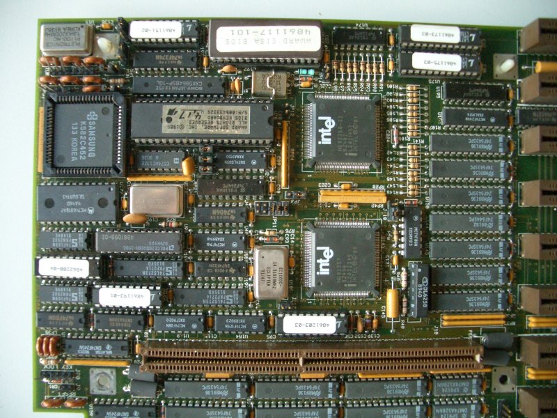
This is the most modern part of the board (as by 1992 standards). It’s actually using ASCIs and not only 80’s-style PLDs. In the top-left corner you’ll spot the Samsung 82C452, which is controlling the 2 serial and 1 parallel port(s) on the board.
Next to it is all the Keyboard/BIOS stuff – one fine thing to mention: Hauppauge used an external battery for the settings/clock. Thanks to god they didn’t use some of those nasty Dallas SRAM/Clock chips. After 10 years the internal battery get weak and there’s no way the replace just that (well, there are ways, but that’s really the last resort).
Now it’s getting serious: ASICs, made by Intel… a chip set! Woohoo! Namely the 82350 Intel chip set (Click here for a lenghty article I wrote about this chip set).
This chip set comprises the 82358-33 EISA Bus Controller (EBC) and the 82357 Integrated System Peripheral (ISP). Together these two devices implement a functional interface to the EISA bus,  and provide most of the standard peripheral functions necessary to implement a minimum EISA solution. In a simple sentence: The EISA interface.
That said, there’s a catch: The 4860 being an early EISA board, does not feature the more ‘modern’ 82358DT EBC you’ll find on most EISA boards. This might be the reason why some EISA cards refrain from working with this board. I found a snippet saying “The 82358DT is a superset of the original 82358 and includes a mode compatible with the 82359 Buffered Bus“. The 82359 DRAM controller is obviously missing (probably not a available at that time) and the RAM controller is implemented in lots’o’GALs.

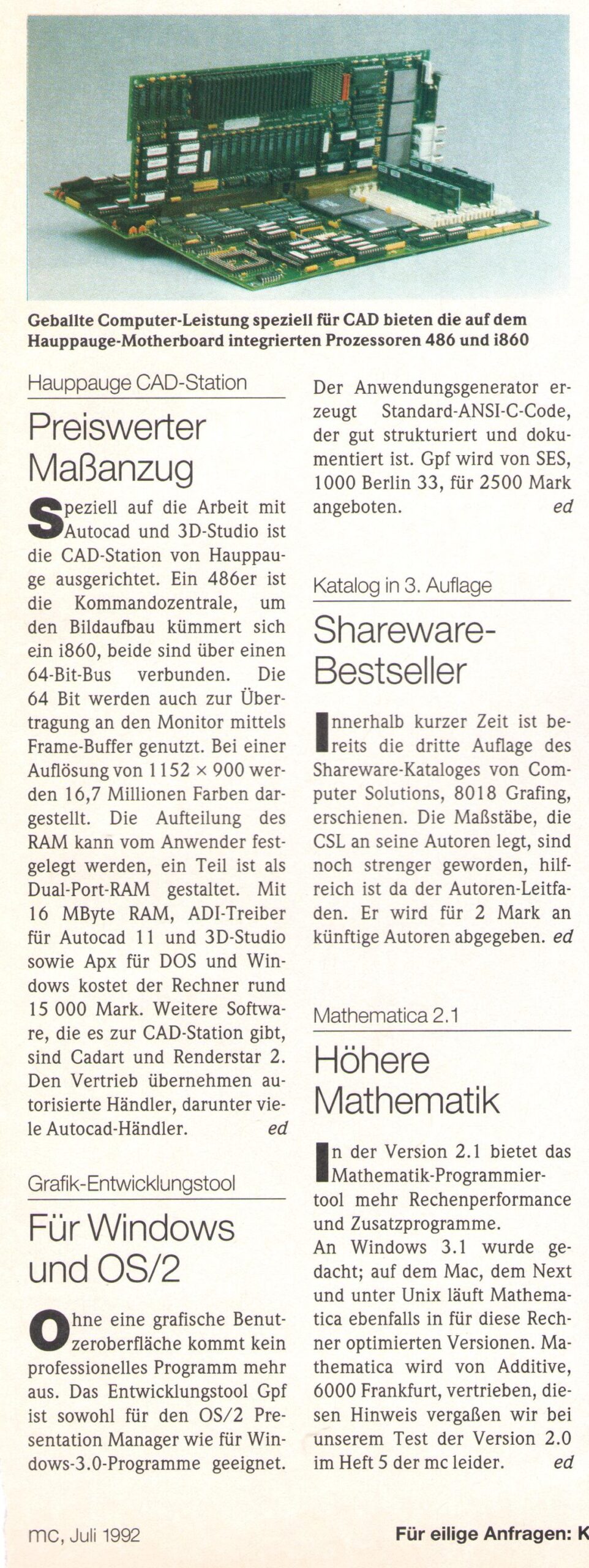
Across the bottom of the picture there’s another slot, looking a bit like EISA… but it’s not! That’s the Hauppauge 64bit Framebuffer Expansion Bus. Hauppauge sold a graphics card basically containing 4MB of VRAM which could be directly accessed by the i860 at very high speed. That made the board a graphics-accelerator like for example the SPEA Fire.

Not much is known about this framebuffer card. Still, I was able to find a blurry press photograph in an 1992 computer magazine. Obviously it’s mainly buffers, GALs, VRAM and 3 RAMDACs for R, G and B… I do have an AutoCAD ADI driver, but I guess you won’t get this board anywhere on the planet anymore 🙁

4860-Framebuffer

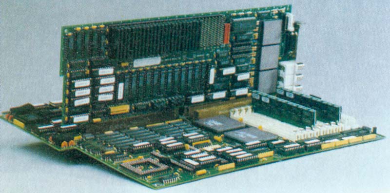
Here’s a better photograph I just dragged out of the web:

4860_vidcard

Upper right

UpperRight

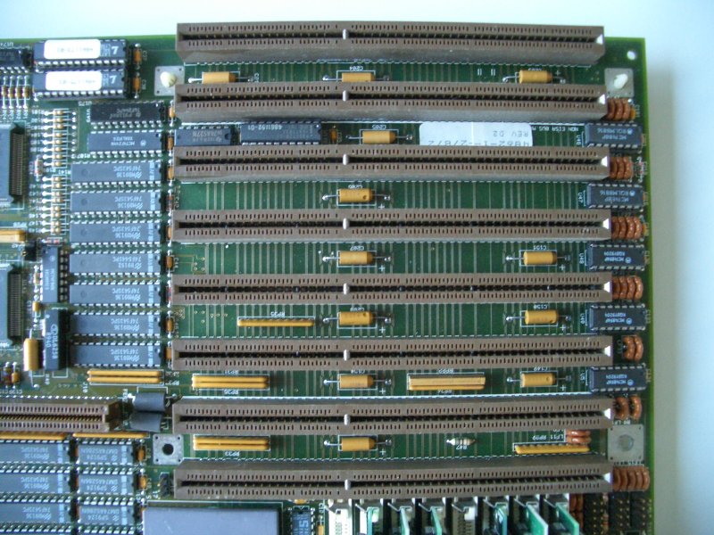
Welcome to the end of our tour… the boring part – at least at the first look. 8 EISA slots and some buffers. Nothing exciting, really.
If you take a close look, you’ll see the sticker between slot 6 & 7 (counting from the bottom). This sticker tells you that this board is a “rev D2”:

RevDetail

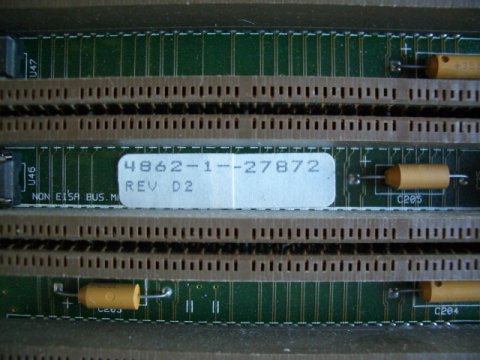
I don’t have that much documents to figure out the tiny little differences to older versions, but the big one is slot #2. In previous revisions, that slot was ISA… a heritage to this fact is, that on REV D2, this slot is a “non EISA bus master slot” – which is also true for slot #7 (inline with the Frambuffer-Card slot).
The reason for this is (my assumption, though) that the 82357 (ISP) integrates seven 32-bit DMA channels, of which 6 routed to the EISA slots and one used for the Framebuffer.

That’s it for now. I will add new findings as I proceed with my fiddlings.
Thanks for joining the tour, don’t forget to buy a T-shirt in the merchandise shop at the exit…

Software

For the whole enchilada, get the 4860 Manual here. That’s real men reading stuff… i860 source code samples included.

This is the official tools and driver disk and here’s a (yet) small archive containing the ADI drivers for the Framebuffer card and the i860 APX specifically tailored to the Hauppauge 4860 (i.e. won’t run on any other i860 system).

Another nice find: The presentation held at Hot Chips Conference 1990. It gives some more insight into the board design and ideas behind it.

Nostalgia

I found a short article in one of my old (German) computer magazines (“MC”, 1992). Here it is for your amusement/riddling:

Microway NumberSmasher

The US company MicroWay (also known for their NDP compiler range), presented an i860 ISA card called NumberSmasher 860.
It was available in two speed grades, costing 11698 DM (@33 MHz) or 14170 DM (@40 MHz). The needed compiler (C, Pascal or Fortran) was an 3135 DM extra.

This 16-bit ISA card featured an 40MHz i860, 4 or 8MB of ram and one INMOS OS-link controlled by a IMSC012 on a litte PCB, hiding 2 additional IMSC012 below it on the main PCB.
It is possible to connect one IMS C012 to to the ISA host bus to “feed” the Number Smasher 860 with programs and data (seedocumentation at the bottom of this page).

Here’s the board in its full beauty:

NumSma860

The left half is occupied by the 8MB RAM. The right half is all bus-logic, buffers and drivers. At the top is a very custom HD-connector – thanks to Jörg Heilmann I now know that this is the FiFo-Connector counting 100 pins. Again thanks to Jörg I also have4 pages of documentation to this connector which was designed to connect the FIFO I/O board (available as ISA and EISA version) to.

On a little separate PCB (having “LINK DR V2.0” printed on it) connected to P3 some sort of additional communication part was placed, consisting of an octal transceiver, one INMOS C012 link-adapter a PAL and an octal buffer featuring two 4-pin connectors (J1 & J2).

  • J1 – GND – GND(code) – to pin 3 of J4 – to pin 3 of J3 – GND
  • J2 – GND – GND(code) – to pin 16 of P3 – to pin 14 of P3 – GND

Additionally there are 3 configuration jumpers – function as far as my measurements go:

  • J3 – Connects pin 18 of the board-connector (LinkIn lower onboard C012) to either LinkOut of the C012 (jumper on upper pin) or to the 4th pin of J1 (jumper on lower pin).
  • J4 – Connects pin 20 of the board-connector (LinkOut lower onboard C012) to either LinkIn of the C012 (jumper on upper pin) or to the 3rd pin of J1 (jumper on lower pin).
  • J5 – Linkspeed for the IMSC012  (upper is 20Mbps, lower is 10Mbps)

NumSma860_Link

Documentation

As I have next to no official documentation about this board I would be very glad to hear from anybody who knows the tiniest bit about this card! AFAIK the original “manual” wasn’t bigger than 13 pages… pretty lame for a board costing as much as a small car back in those days.

Thanks to Jörg Heilmann, I got my first piece of original documentation: The 100 pin FIFO-Connector is described on these four pages. Not much but a start!

Here’s what I found out about the P3 connector on the board, having the “LINK DR” PCB plugged into it. If you have a look at the picture above, I’m start counting pins from bottom right continuing zig-zag like this:

26 oooo...oooo 2
25 oooo...oooo 1

1 – VCC
2 – CLK 5MHz
3 – Reset of the C012 (Pin 11) goes directly to the i860 reset-pin
4 – GND
5 – D7 from ISA Bus
6 – D6 from ISA Bus
7 – D5 from ISA Bus
8 – D4 from ISA Bus
9 – D3 from ISA Bus
10 – D2 from ISA Bus
11 – D1 from ISA Bus
12 – D0 from ISA Bus
13 – ???
14 – Pin 2 of the upper onboard C012
15 – ???
16 – Pin 1 of the upper onboard C012
17 – ISA Pin B8 (NoWS)
18 – Pin 2 of the lower onboard C012
19 – ???
20 – Pin 1 of the lower onboard C012
21 – MEMW to ISA
22 – MEMR to ISA
23 – ???
24 – ???
25 – VCC
26 – GND

From these findings I conclude that J2 is directly connected to the upper onboard C012 while J1 is either connected to the lower onboard C012 (J3 & 4 set to upper pins) or to the C012 on the LINK DR (J3 & 4 set to lower pins) which has its data-lines connected to the ISA bus.

On the main-card are 3 other jumpers:

  • J1 & J2 – Set the connection speed of the two C012 on the card
  • J3 – Select the ISA IRQ. Top down: IRQ 10, 11, 12, 15.

Everything else I have for now is a single article from the German computer magazine “c’t” (3/91,p.164 by O. Grau and A. Stiller) giving a bit more insight in the way the card works:

“Das Interface zum ISA-Bus des Hostrechners ist auf einer kleinen austauschbaren Platine untergebracht und basiert auf einem FIFO. Durch ihn geht sämtlicher I/O. Ein vergleichsweise aufwendiges Protokoll sorgt für einen recht langsamen Datentransfer, so besteht jeder Transfer aus dem Kennbyte 0 (Schreiben) oder 1 (Lesen), gefolgt von der Zieladresse (vier Bytes) und dem Datum (vier Bytes).”

The interface to the hosts ISA-bus is located on a small changeable board and is based on a FIFO [buffer]. All I/O is going through this. A comparably complex protocol is the reason for the data transfer being a bit slow. Each transfer consists of a ID-byte (0=write, 1=read) followed by the target address (four bytes) and the data (four bytes).

This “protocol” sounds very familiar to me. INMOS had the same, calling it PEEK and POKE… I’m still evaluating this, so stay tuned.

[11/05/10] Great News! I had some time and did some deeper investigation… hardware archaeology at its best 😉 So read on in the next post… it’s dissection time!