Tag Archives: interface

T2A2 for everyone

While the guys over at OpenApple were speculating in their latest podcast what a Transputer actually is… well, there are about a 100 links and ways on this page to find out – but hey… just click here – and of course that box saying search would do great wonders, too.

But seriously, my bad: I should have mentioned that this page your looking at is really just one post of many… so make sure you start at a Chapter (Menu. At the Top. ↑…yes up there) and read them in the order you’d read a book 😉

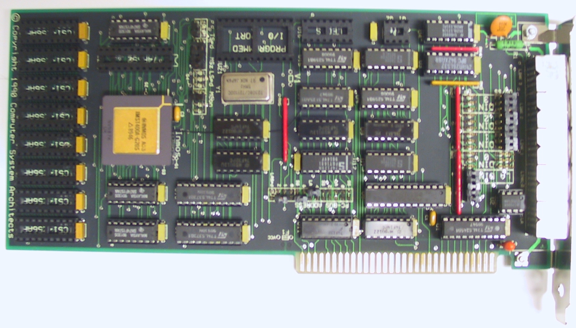
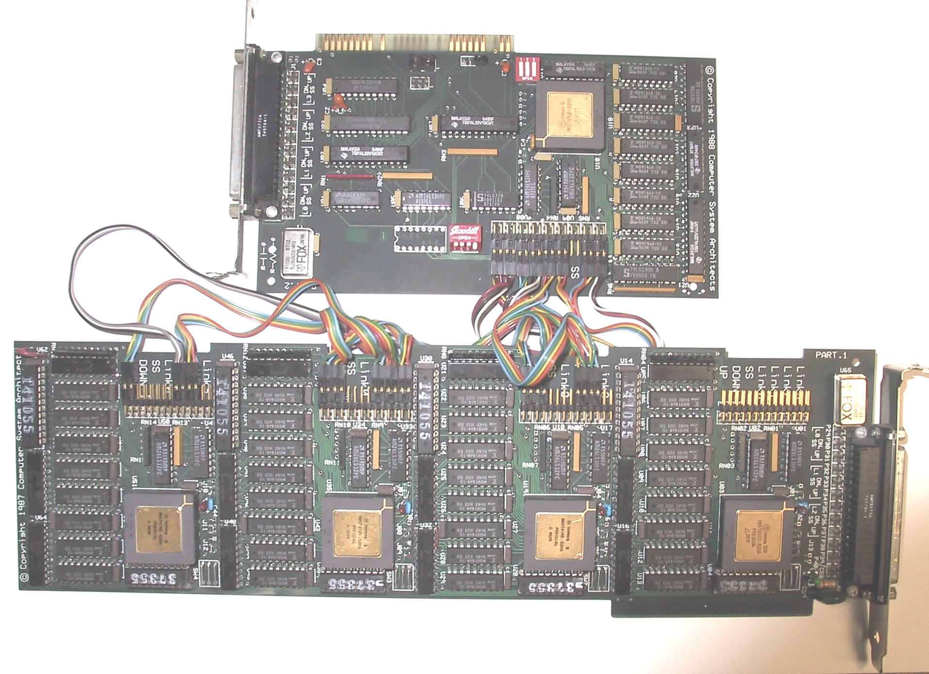
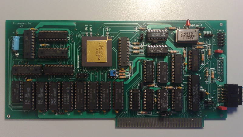
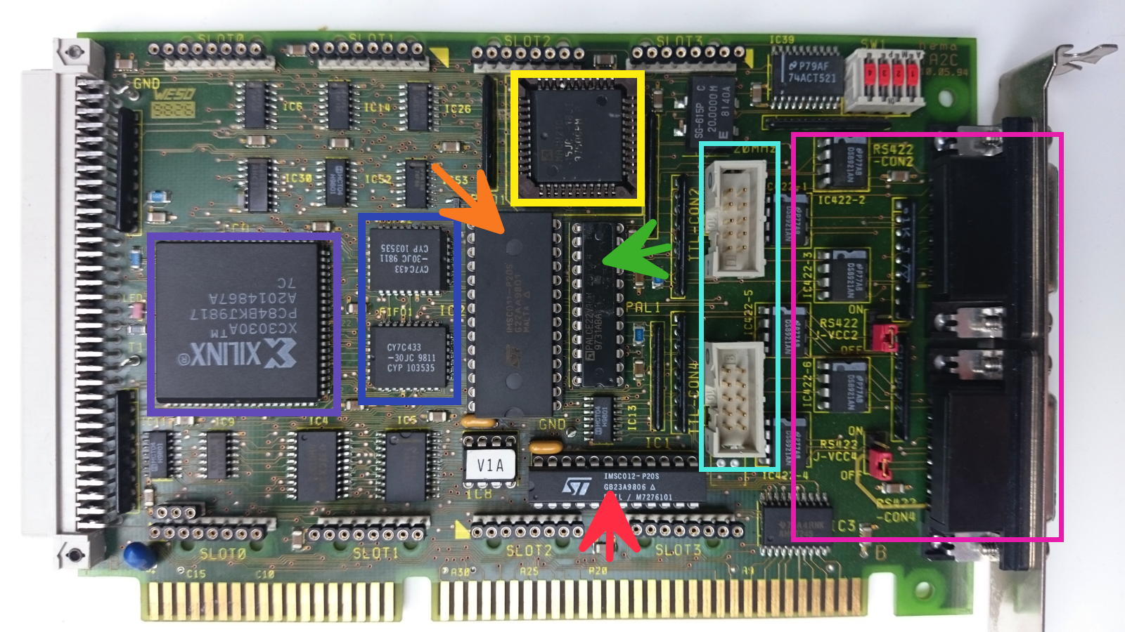
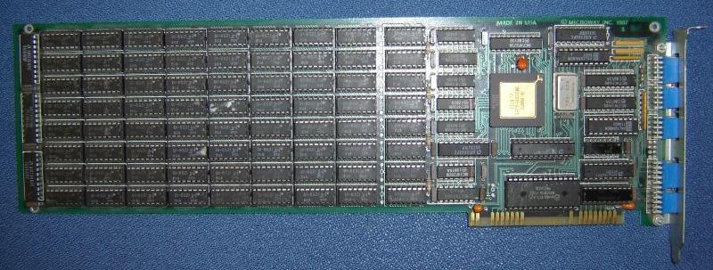
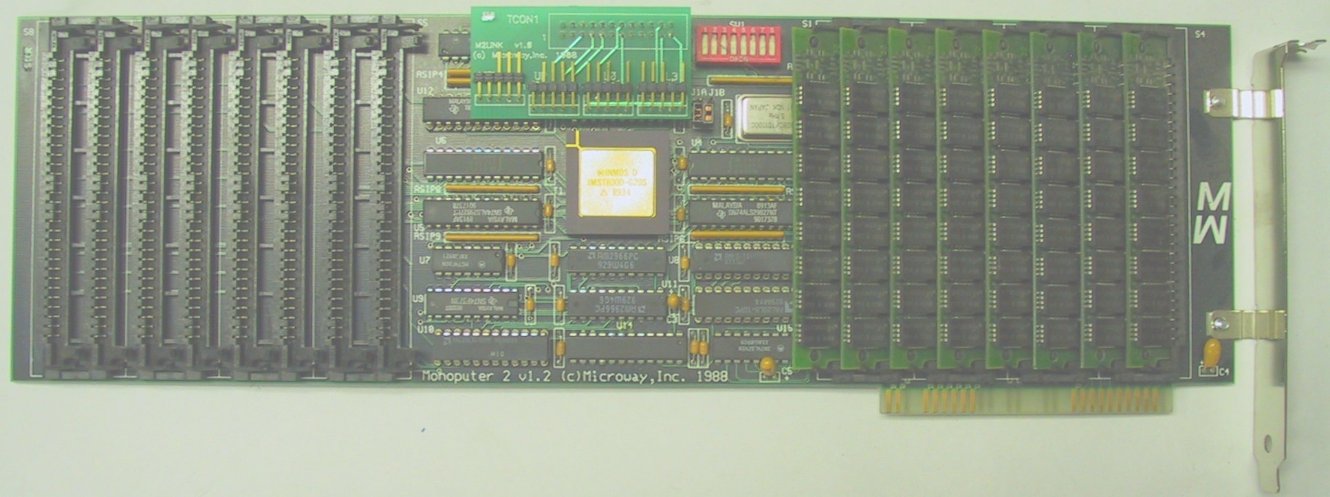
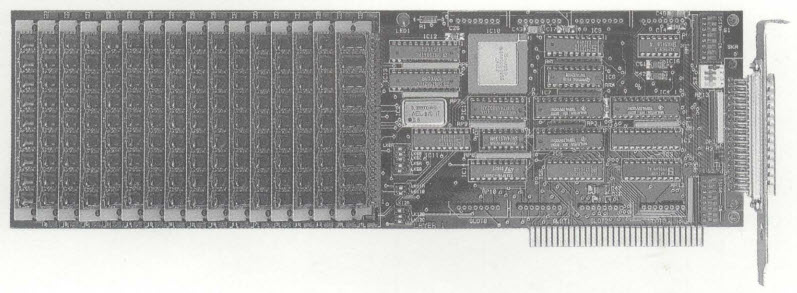
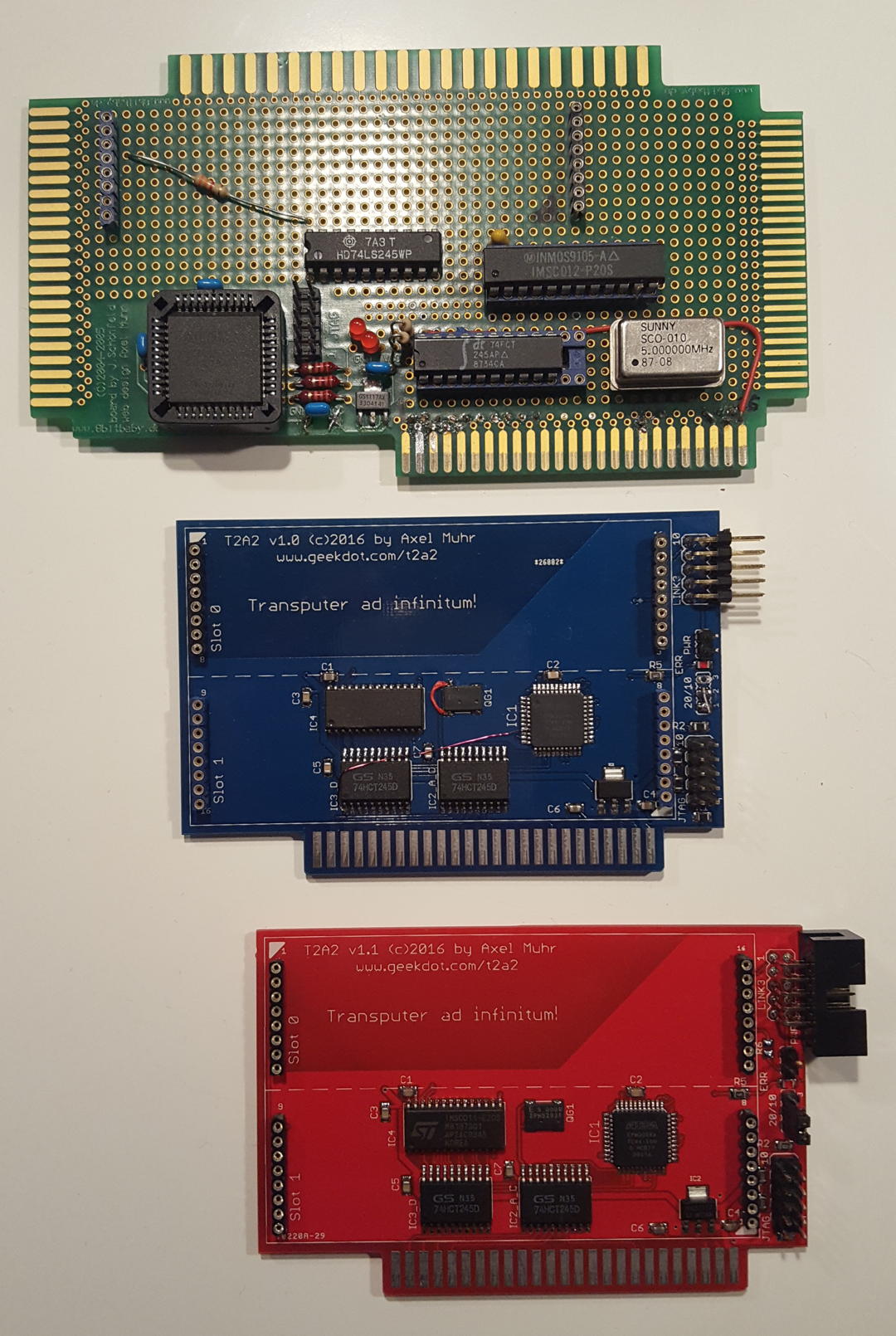
After quite some years (and a handful Apple II users requests) I felt the urge to finally put the T2A2 prototype (read that post to get a more general understanding) into a real expansion card… and here it is: Say “Hello!” to the T2A2 version 1.1!

It came a long way…

t2a2_evolution

…in more detail:

t2a2_front

As you can see, the final T2A2 is much smaller than the prototype (which used an 8bit Baby one-for-all PCB) and offers many additional features

  • 2 size-1 TRAM slots (or one size-2) – double the processing power!
  • Low-power, low-profile parts used where possible (3.3V CPLD, HCT logic)
  • External Transputer-link available as edge connector – extend your network to “near infinitum
  • Jumpers for LinkSpeed and optional power to the Transputer-link connector
  • Fully buffered to be a good Apple II bus citizen
  • Works in any slot set to “your card”

Beyond this, everything said about the prototype is still true.

Most important:

a) It’s not tested in the ][ or ][+. I simply don’t own one of those.
Update: One owner reported it’s perfectly working in his IIe!
b) The T2A2 won’t instantly speed up any of your Apple II[e/gs] applications.

It’s more like a co-processor attached to it. And even then, you’ll need something really calculation-intensive to justify the time you’ll loose due to communication between the Apple and the Transputer. A single square-root for example wouldn’t make much sense – but having a complex algorithm (like the Mandelbrot fractal in my demo)  does absolutely make sense, as you just pass the parameters to the Transputer and let him do the sweating.

But on the other hand, FPU cards like the Innovative Systems FPE (using an M68881) or my even faster clone “NumberCruncher Reloaded” did just send instruction by instruction. So I somehow fancy the idea writing a SANE driver for GS/OS to integrate the T2A2 more transparently.

Want your own T2A2?

So now you’re keen to get one yourself? Please check this list first:

  • Do you have a TRAM already? (*)
  • You are aware that there’s no real software (yet) besides my little Mandelbrot demo?
  • You are keen to program something yourself – or are fine to wait until somebody else did?

While the Apple II side of coding is pretty easy, you have to get a grip about the Transputer development, too. That includes a DOS/Windows (<=XP) setup and some knowledge of C and/or OCCAM. I’ve created a little Transputer “SDK”, namely a VirtualBox image running DOS.

Plenty of Dev-Docs are available here.  
I suggest using the INMOS cross-compilers for C or OCCAM. An alternative C compiler came from LSC, which might suit you more if you don’t like the INMOS stuff.

Ok, so you’re still with me… so I have the first batch of 20 T2A2 PCBs ready which I will populate on-demand, and for 40€ (plus shipping) one of them can be yours.
(*) I might be able to offer you a TRAM, too. The price depends on available model, RAM size and CPU used.

⇒ drop me a mail tonobody likes SPAM
(Sorry, you have to type that into your mail-client – nobody likes SPAM, so do I)

Also check the T2A2 forum for current availability, shipping procedure and built status.

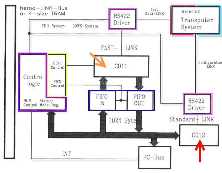
Some more technical details

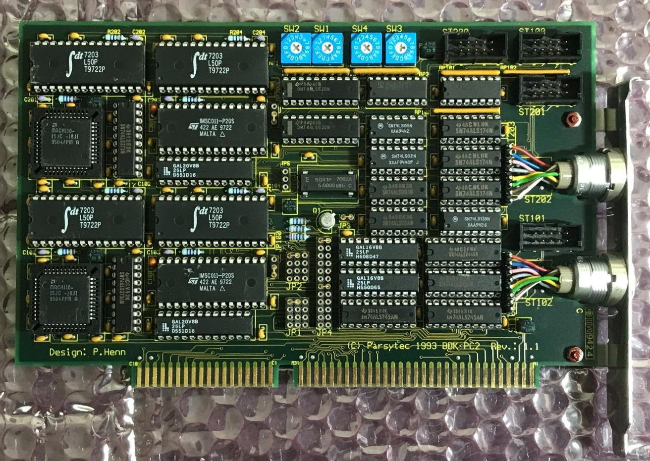
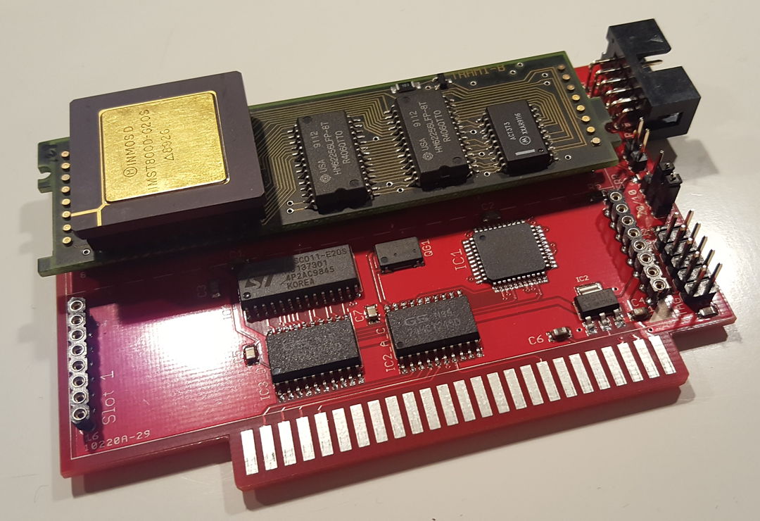
Here’s a T2A2 with a size-1 TRAM installed in Slot-0:

t2a2_with_tram

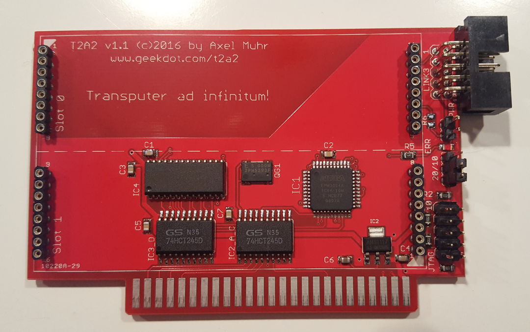
The T2A2’s CPLD programming can be updated any time through a JTAG port (the lower 2×5 pin-row at the edge).
The jumper above it can be used to set the linkspeed for the TRAMs (10 or 20mbps). If you look very close, there’s a tiny LED next to that jumper. It’s the error LED controlled by the CPLD.
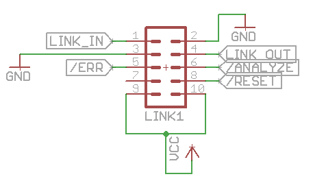
The next single jumper enables the VCC pins on the external Link connector, meant for (small!) external extensions. This connector is the same used on the Gerlach card and is very convenient because of its ubiquitous standard 2×5 shrouded pcb header connector. Here’s the pinout:

As said, the V1.1 T2A2 offers two size-1 TRAM slots. Before plugging in 40MIPS of raw processing power consider the amount of juice being pulled there. Depending on the amount of RAM and load a single TRAM can use up to 800mA of power!  😯
Given the max. of 4A on a standard IIgs power-supply, two TRAMs could bring your souped-up GS into trouble… it’s better to use the external connector with just one smaller TRAM or even simply bridge the Link0In/Out pins with Link3In/Out so that the T2A2 works as a TRAM-less adapter.
That said, there are size-2 TRAMs in existence which will snugly fit  and won’t hurt that much.

Other Transputer interfaces

This is the collection of other Transputer interfaces and cards (i.e. not from the usual suspects) I came by here and there. And no, I don’t actually own them all.
Some are rare, some are odd, may are cool and most are all three of them 😉

This post will be irregularly updated as new finds come along…

Pixar Transputer Card

Yes, that’s true. Pixar built its own Transputer interface back in the days, simply called “Render Accelerator”. Nomen es omen 😉
In constant search of raw computing power they tried out everything, eg. Intels i860 and others. It was just another logical step to try speeding-up Pixars Renderman package by using a Transputer farm. As an early adopter, they had to build their own stuff to suit their demands. Here’s a very interesting read about the long way Renderman came from and which hardware they’re were using. This article about texturing techniques is mentioning this card on pp.16.
The mentioned Jeffrey Mock was also quite busy during his Pixar days in helping Logical Systems (LSC) by writing a concurrency library for their C-Compiler.

Here’s the front of the full-size 8bit ISA card – filled up to the brim.
It features two T800-20 Transputers, each having its own 4MB of RAM. Two links are facing the outside-world – I presume it’s been meant like a up- and down-link to the next card.
The rest is standard early-days ISA bus, C012, Transputer DRAM design.

pixar_transputer_card1

No much to say about the back side. The silkscreen is a bit uncommon, but it’s nice when it comes down to repairing… and some “burning” shows, that seemed to be the case with this specific card.

pixar_transputer_card2

The Quintek T9

This is a very manly approach into transputing matters… don’t give me that step-by-step upgrading of an Transputer array. Just do it once and do it right 😉

Quintek_9T

Yes, that’s 9 Transputers, each with 1 or 4MB RAM and a C004 all directly soldered onto that 8-bit ISA card. It sure was expensive…
While there’s a C004 (the 6th golden IC from left), there’s no T2xx to control it. So I assume that one of the T800 is in charge to configure it… or this is done through the ISA link-interface as there are two C012 on the card,

The YARC ProTran

This is a fullsize 16-bit ISA card from YARC. It features 4 Transputers with the option of supporting them with a (for the time) big amount of RAM.

YARC-ProTran

The ProTran board can be equipped with 1 to 4 Transputers. The root Transputer (the rightmost) can have acces to 1-16 megabytes of RAM – it’s 8 in this picture. Each of the other three can be configured with 1 to 8 MB. That was very serious stuff back then.
What’s most interesting about this card is that YARC  didn’t gave much about standards and went a proprietary route in many places:

  • A proprietary bus interface is said to provide a peak I/O speed exceeding 1 MB/sec
  • All links, event inputs and subsystem control signals are fed to a proprietary pin-field array.
  • The memory design uses a multibank and interleaving technologies to achieve zero wait state performance

All this explains the excessive use of GALs in the lower half of the card. Beside the proprietary approach the ProTran offered a compatibility mode (read: B004 interface) to use standard INMOS tools.

CSA

CSA (Computer Systems Architects) was big in the educational market and produced smaller, better integrated B004 compatible Transputer cards. The higher integration of DRAM parts allowed half-length ISA cards meant for evaluation or as a starting point for building bigger systems later.
(The following pictures are courtesy “the PCPUTER” page. Permission to repost them were kindly granted)

Meet the “Transputer Kit PC Card” –  They came bundled with a slightly restricted version of the Transputer Toolset, together with a great manual which described lots of different programming and hardware interfacing lab-type experiments.  These cards used standard multi-pin circular DIN connectors/cables to route the link and reset signals, and provided the first hands-on introduction to distributed parallel processing for many people.  They included a “budget” T400A 32 bit non-floating point processor, and off-processor memory was an option

CSA Kit Board

This is th PART.1 four processor board – mainly a carrier for CSAs proprietary Transputer Modules (like INMOS’ TRAMs), and the single processor PART.2 board featuring a PC interface.

CSA PART1 and PART2 System

The “Gerlach card”

The card from the book “Das Transputerbuch” from A. Gerlach is a typical example. It has its own post on this page.<
Very simple design but only 2 layers and completely documented in the book.

Gerlach

Parsytec BBK PC-2

As ususal, Parsytec did things a bit different than most others.
Their ISA interface “BBK PC-2”  has two RS422 interfaces using their ‘standard’ Lemo connectors (see the the post about the x’plorer for more about these)
All Parsytec interfaces, no matter which bus-system were called BBK and having a number attached, telling you how many link interfaces were provided, e.g. the Sun SBUS card was called BBK-S4…

Like the HEMA card, this one has SRAM buffers, too. Also it looks like it’s using a 16-bit interface to the ISA bus.

Ingenieurbüro Ingo Mohnen (aka “IB Mohnen”)

This “engineering office” is pretty unknown in the already small Transputer community, even more outside Germany.
But they did very sophisticated Transputer interfaces. Actually they were the OEM for Parsytecs PCI BBK but offered other cards, too.

For example the PCI-008 series. Obviously a IMSB008 for the PCI bus. I have pictures of the V2.0:

…and V3.1:

Both versions seem to be primarily meant as OS-Link interface, while they offer space for an onboard Transputer and RAM both weren’t populated with these.
V3.1 also seem to implement the C011 into the FPGA while switching back to a PGA Transputer while having used a TQFP package in version 2.

Then there was the already mentioned BBK line of cards. Starting with the BBK-PCI light of which I don’t have a better picture than Ram does on his page (Fun fact: Also Sundance OEM’ed this card from IB Mohnen). Basically it’s a IMSB004 compatible interface for PCI. Sweet, want one!

The bigger brother is the BBK-PCI, featuring 4 full blown OS-Links and acting as PCI bus-master. Definitely the high-end of PCI link-interfaces. I do own one of these but need to make some nice photos… so in the meantime use the link to Rams page 😉

Hema TA2

The Hema TA2 is some very special specimen of ISA interface cards. IMHO it’s the last and most sophisticated interface you can run in an ISA bus. These are the feature highlights:

  • 16 bit ISA interface
  • half-size card
  • 4 TRAM sockets
  • TTL and RS422 link connectors (if RS422 drivers are fitted, TTL is not usable)
  • B004 compatible ‘Fast Mode’ as well as 100% vanilla ‘Slow Mode’

The TA2 implements an Idea which can be found in some documents from those days, about getting the maximum speed from the sluggish ISA bus and a link-interface chip like the IMS C011/012:
Overlapping acknowledge by using FIFO buffers and a controlling FPGA.

This is how the TA2 looks like:

HemaTA2

I’ve marked the the important parts with colors/arrows:

  • red arrow – the IMS C012
  • orange arrow – the IMS C011 connected to
  • blue – two 1KB FIFOs controlled by
  • yellow – a MACH 110 CPLD and
  • green arrow – a PAL
  • purple – a XILINX 3030 FPGA doing the control logic
  • cyan & magenta – TTL and RS422 link connectors

And here’s the block-schematic using the same colors:

TA2_Block

The schematic also mentioned the two other cool features of the Hema TA2:
Four TRAM slots and the “hema LINK-Bus”, a proprietary two row DIN 41612 connector which provides all links/subsystem which were used otherwise by the 4 TRAMs.
Finally there is a 4-bit microswitch (upper right corner) to set a unique ID for the card so you can identify up to 16 cards in a single system.

Software

Using the provided control program “CTA2” everything can be set by software, e.g.

  • Base addresses for the fast- and slow link (0x150/0x158 by default)
  • Swapping fast/slow link configuration
  • Linkspeed for every link (fast/slow/TRAM/hema-bus)
  • Up- /Down-subsystem control
  • Interrupts per link
  • Waitstates

All the hardware wise ‘jumping through hoops’ still doesn’t do the job alone. To reach the ultimate ISA speed (the docs are talking about up to 1mbps) the communication needs to be tuned, too.
Lets talk a bit x86 assembler here (ahhhh), and DOS-only for sure:
It’s not enough to use simple in and out port instructions and constantly poll the C011/12 status register – that’s way too slow. You’ll need to go for the string variant(s) ins[b|w|d] combined with the rep instruction. Here’s an example for a C insb wapper function:

void insb(UINT16 port, void *buf, int count)
{
   _ES = FP_SEG(buf);   /* Buffer Segment */
   _DI = FP_OFF(buf);   /* Buffer Offset  */
   _CX = count;         /* Bytes to read  */
   _DX = port;          /* from Port xy   */
   asm   REP INSB;
}

Same goes for outs[b|w|d] respectively.  But there’s another extra to care for: The TA2 provides special  registers to give you deeper insight into its status, e.g. FiFo fill-rate (empty, half-full, full), FiFo interrupt settings.
So in effect, you couple the fast ins/outs instructions with interrupts attached to e.g. input half-full and output full.

That said, there are some caveats. ins[b|w] and outs[b|w] are supported from the i8018x and V20 on.  insd and outsd needs a 386.
And then there are possible speed penalties with 32nit processors (i.e. 386 and up) as they optimized the port instructions for virtualization (Virtual 8088 mode, not todays VM!) resulting in 100+ cycles per call.

So when everything is 100% optimal, hema says in its documents these are the possible transfer speeds to reach:

Function/Array size 1K 10K 100K 1MB
Read FiFo 150kB/s 390kB/s 570kB/s 615kB/s
Read Polled 160kB/s 160kB/s 160kB/s 160kB/s
Read Direct 600kB/s 610kB/s 610kB/s 610kB/s
Write FiFo 565kB/s 600kB/s 610kB/s 610kB/s
Write Polled 160kB/s 160kB/s 160kB/s 160kB/s
Write Direct 610kB/s 610kB/s 610kB/s 610kB/s

FiFo – Using interrupts and syncing status of fill level.
Polled: Each byte is synchronized with the C012 status
Direct: Like FiFo but no syncing.

Well, this has to be proved yet. Seem I need to write a benchmark… someday 😉

Inmos B004

I’d call the Inmos B004 the “mother of all Interface cards”, simply because it was the first ISA card sold by INMOS. And it wasn’t just the card but it also defined the (PC) standard of the software interface, mostly called the “B004-interface”. What a surprise 😉

So being the first card, it is quite big (full ISA length) while not offering really impressing specs: 8bit XT Bus, just one Transputer –TRAMs weren’t invented yet- and a max. of 2MB RAM (DILs). To do it justice, the manual rightfully calls it “Evaluation Board” and for that purpose it’s totally fine – remember that 2MB were quite an amount of RAM back in 1984.
To create a multi-Transputer network you had to either plug-in multiple B004s or connect an external network to the onboard connectors (the blue ones in the picture below).

As mentioned, the B004 software interface is what makes this card a keystone in the Transputer universe. All communication to the host (i.e. the XT/AT compatible PC) is done through a port range normally beginning at 0x150 (base, can be moved by some cards).
With certain offsets the host software can communicate with the Transputer, or the C011 to be precise:

Base Address Register Comment
+0x00 C011/12 input data  read
+0x01 C011/12 Output data write
+0x02 C011/12 input status register read = returns input status
write = set input interrupt on/off
+0x03 C011/12 Output status register read = returns output status
write = set output interrupt on/off
+0x10 Reset/Error register write: Reset Transputer & C011/12 and possibly subsystem (check manual)
read: Get Error status
+0x11 Analyse register  (un)set analyse

This mapping was used by more or less all ISA interface cards and extended by other more sophisticated interface cards later.

Clones

Needless to say, that very soon there were a couple of “inspired” models from other manufacturers. AFAIK all of them support Transputers up to 30MHz, which the B004 didn’t… so they’re actually better.

This example is from Microway (yes, those guys who later build the i860 Number Smasher), named Monoputer and dated 1987. Up to 2MB could be used on it. Mind the connectors being accessible from the outside:

Microway-B004

Later they produced the “Monoputer 2” which was more modern and used SIMM RAM modules instead of DIL parts. The Transputer and Linkinterface moved into the middle of the card and the link connectors were moved inside the pc case again – the connectors are the very same used on the NumberSmasher860:

monoputer2

And here’s the one Transtech made, calling it TMB04 mind the SIMM banks which enable the card to give home up to 16MB RAM (at 3 cycle speed!):

Transtech TMB04