Category Archives: Number Smasher 860

Microway NumberSmasher

The US company MicroWay (also known for their NDP compiler range), presented an i860 ISA card called NumberSmasher 860.
It was available in two speed grades, costing 11698 DM (@33 MHz) or 14170 DM (@40 MHz). The needed compiler (C, Pascal or Fortran) was an 3135 DM extra.

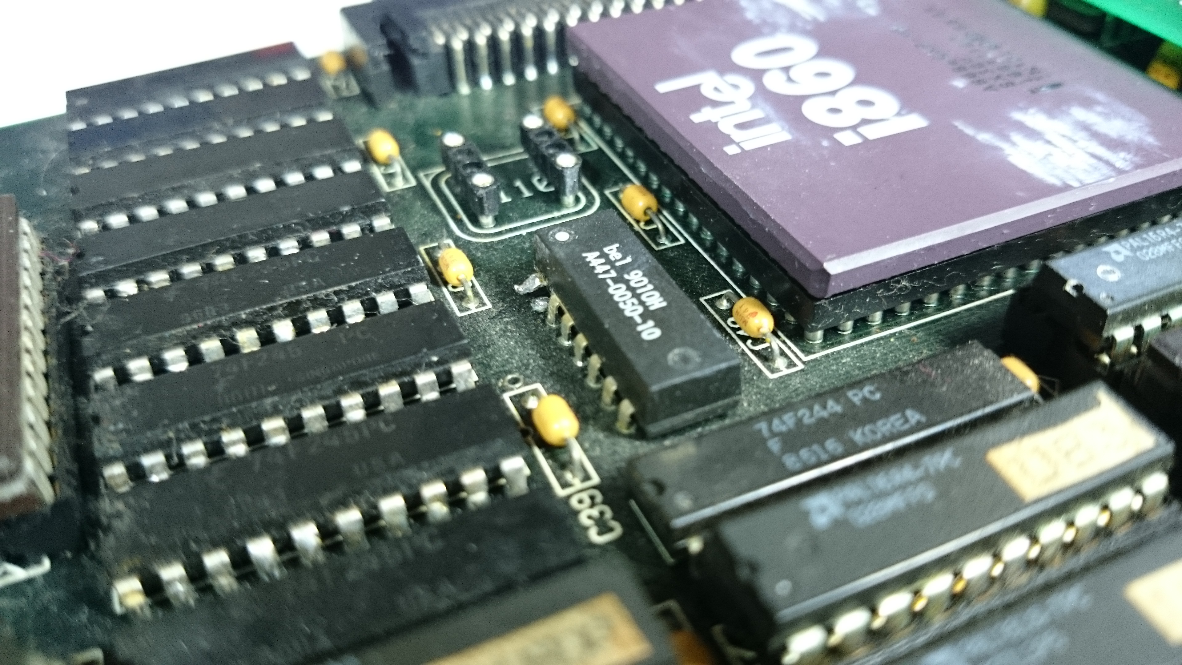
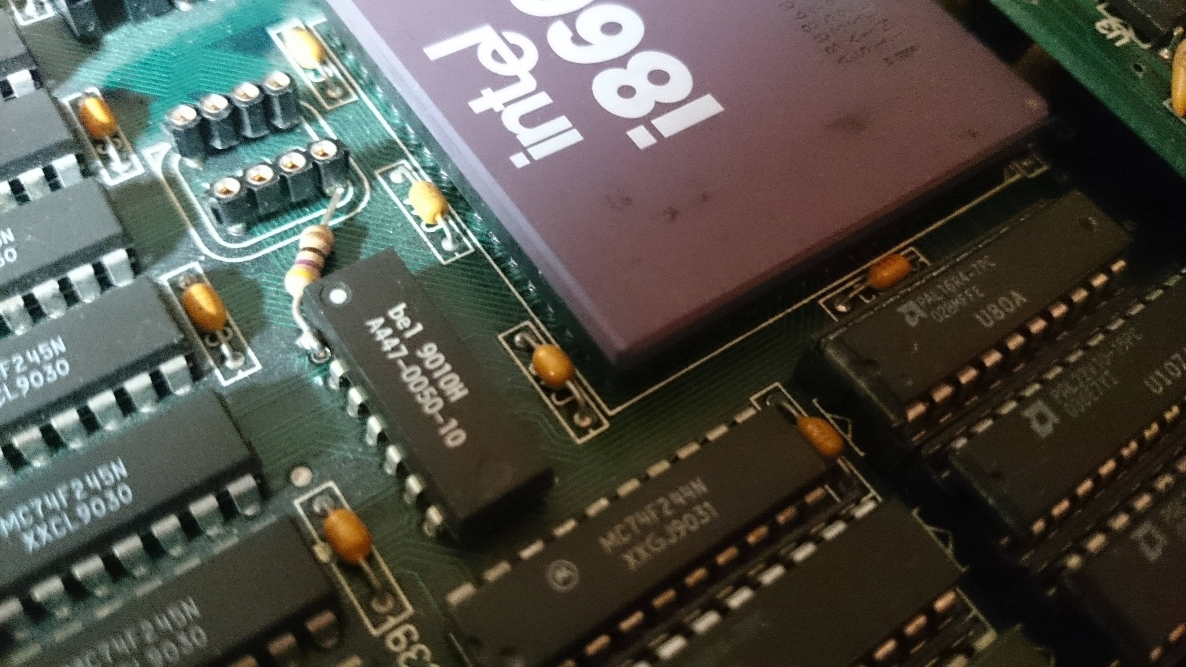
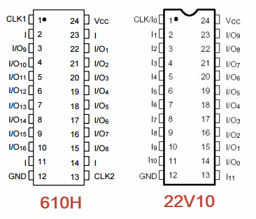
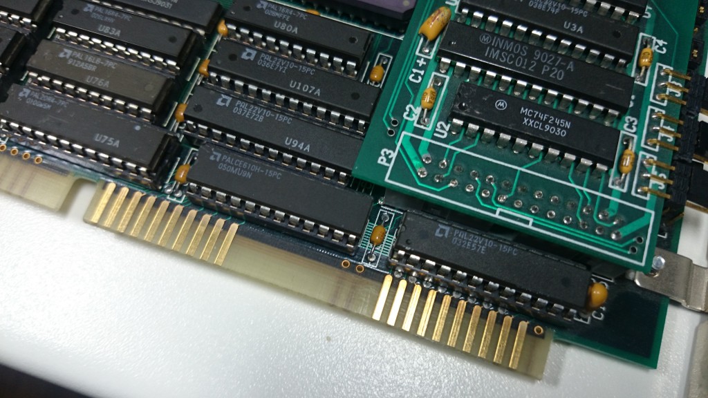
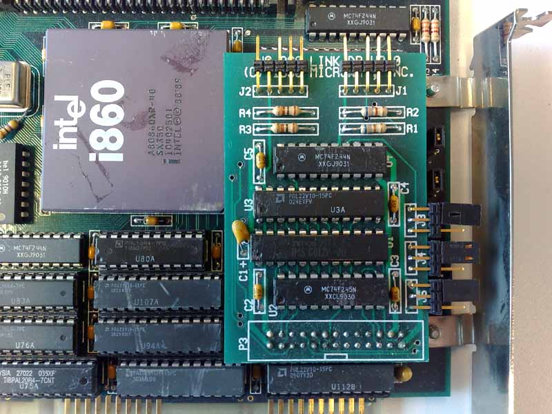
This 16-bit ISA card featured an 40MHz i860, 4 or 8MB of ram and one INMOS OS-link controlled by a IMSC012 on a litte PCB, hiding 2 additional IMSC012 below it on the main PCB.
It is possible to connect one IMS C012 to to the ISA host bus to “feed” the Number Smasher 860 with programs and data (seedocumentation at the bottom of this page).

Here’s the board in its full beauty:

NumSma860

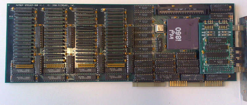
The left half is occupied by the 8MB RAM. The right half is all bus-logic, buffers and drivers. At the top is a very custom HD-connector – thanks to Jörg Heilmann I now know that this is the FiFo-Connector counting 100 pins. Again thanks to Jörg I also have4 pages of documentation to this connector which was designed to connect the FIFO I/O board (available as ISA and EISA version) to.

On a little separate PCB (having “LINK DR V2.0” printed on it) connected to P3 some sort of additional communication part was placed, consisting of an octal transceiver, one INMOS C012 link-adapter a PAL and an octal buffer featuring two 4-pin connectors (J1 & J2).

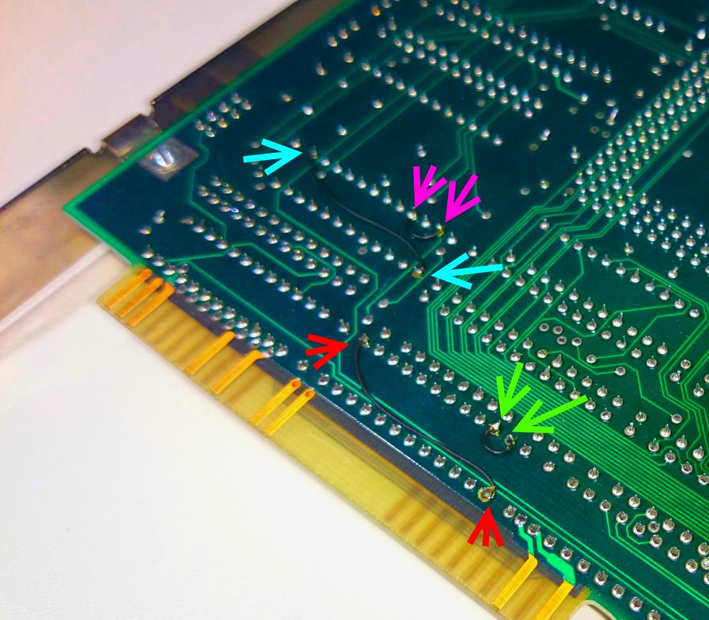
  • J1 – GND – GND(code) – to pin 3 of J4 – to pin 3 of J3 – GND
  • J2 – GND – GND(code) – to pin 16 of P3 – to pin 14 of P3 – GND

Additionally there are 3 configuration jumpers – function as far as my measurements go:

  • J3 – Connects pin 18 of the board-connector (LinkIn lower onboard C012) to either LinkOut of the C012 (jumper on upper pin) or to the 4th pin of J1 (jumper on lower pin).
  • J4 – Connects pin 20 of the board-connector (LinkOut lower onboard C012) to either LinkIn of the C012 (jumper on upper pin) or to the 3rd pin of J1 (jumper on lower pin).
  • J5 – Linkspeed for the IMSC012  (upper is 20Mbps, lower is 10Mbps)

NumSma860_Link

Documentation

As I have next to no official documentation about this board I would be very glad to hear from anybody who knows the tiniest bit about this card! AFAIK the original “manual” wasn’t bigger than 13 pages… pretty lame for a board costing as much as a small car back in those days.

Thanks to Jörg Heilmann, I got my first piece of original documentation: The 100 pin FIFO-Connector is described on these four pages. Not much but a start!

Here’s what I found out about the P3 connector on the board, having the “LINK DR” PCB plugged into it. If you have a look at the picture above, I’m start counting pins from bottom right continuing zig-zag like this:

26 oooo...oooo 2
25 oooo...oooo 1

1 – VCC
2 – CLK 5MHz
3 – Reset of the C012 (Pin 11) goes directly to the i860 reset-pin
4 – GND
5 – D7 from ISA Bus
6 – D6 from ISA Bus
7 – D5 from ISA Bus
8 – D4 from ISA Bus
9 – D3 from ISA Bus
10 – D2 from ISA Bus
11 – D1 from ISA Bus
12 – D0 from ISA Bus
13 – ???
14 – Pin 2 of the upper onboard C012
15 – ???
16 – Pin 1 of the upper onboard C012
17 – ISA Pin B8 (NoWS)
18 – Pin 2 of the lower onboard C012
19 – ???
20 – Pin 1 of the lower onboard C012
21 – MEMW to ISA
22 – MEMR to ISA
23 – ???
24 – ???
25 – VCC
26 – GND

From these findings I conclude that J2 is directly connected to the upper onboard C012 while J1 is either connected to the lower onboard C012 (J3 & 4 set to upper pins) or to the C012 on the LINK DR (J3 & 4 set to lower pins) which has its data-lines connected to the ISA bus.

On the main-card are 3 other jumpers:

  • J1 & J2 – Set the connection speed of the two C012 on the card
  • J3 – Select the ISA IRQ. Top down: IRQ 10, 11, 12, 15.

Everything else I have for now is a single article from the German computer magazine “c’t” (3/91,p.164 by O. Grau and A. Stiller) giving a bit more insight in the way the card works:

“Das Interface zum ISA-Bus des Hostrechners ist auf einer kleinen austauschbaren Platine untergebracht und basiert auf einem FIFO. Durch ihn geht sämtlicher I/O. Ein vergleichsweise aufwendiges Protokoll sorgt für einen recht langsamen Datentransfer, so besteht jeder Transfer aus dem Kennbyte 0 (Schreiben) oder 1 (Lesen), gefolgt von der Zieladresse (vier Bytes) und dem Datum (vier Bytes).”

The interface to the hosts ISA-bus is located on a small changeable board and is based on a FIFO [buffer]. All I/O is going through this. A comparably complex protocol is the reason for the data transfer being a bit slow. Each transfer consists of a ID-byte (0=write, 1=read) followed by the target address (four bytes) and the data (four bytes).

This “protocol” sounds very familiar to me. INMOS had the same, calling it PEEK and POKE… I’m still evaluating this, so stay tuned.

[11/05/10] Great News! I had some time and did some deeper investigation… hardware archaeology at its best 😉 So read on in the next post… it’s dissection time!

Dissection time!

Ok, as I’m probably the last person on this planet fiddling around with the NumberSmasher i860, it was either “help yourself” or bust.

Given the fact that there’s an INMOS C012 on the card I tried my luck with the standard address of 0x150 and checked it with DOS’ crappy old ‘debug’. To my surprise I was able to talk to the C012, so it was very worth to investigate further.
So out went the good ol’ EPROM programmer and the EPROM of the card was dumped into a file.
I have 3 of those boards, two having a label on the EPROM saying “v1.1” and “BOOT_B2”. Both are identical… if you happen to own a NumberSmasher with a different label, get the dumpfile here for comparison.

That was easy, now the harder part: Disassembly. I had to revive my i860 machine language skills again, so it took me 2 days (on and off) to get a full understanding, what’s happening in there.
For those i860 assembly geeks among you, here‘s the fully commented code.

This “BIOS” is actually pretty simple. It’s just what I’d call a “PeekPokeStarter”. The main loop is waiting for a ‘command’ coming in by the way of the C012. This command can be either “0” or “1” as mentioned in the article on the previous page.

“0” means POKE (ie. write) and expects 4 bytes for the address and 4 bytes of data to be written (Both LSB first, Intel-style). So the full command reads: 0 00 00 00 20 78 56 34 12 or “write to address 0x20000000 the value 0x12345678”

So in consequence “1” means PEEK (ie. read) which just needs 4 bytes for the address to be read. The command would then be 1 00 00 00 20 or “read from 0x20000000”. The “BIOS” will then put 4 bytes to the C012 port at 0x150, which requires 4 reads from the PC side getting “78”, “56”, “34” and “12”.

Pretty simple, huh? But how can I start a program after it’s been painstakingly poked into the NumberSmashers RAM? Here’s the trick:

Poking to address 0x00000000 means start from the address given as data. E.g. “write to address 0x00000000 the value 0x20000000” is actually “start from 0x20000000”, or as command-chain: 0 00 00 00 00 00 00 00 20 – so beware of poking to 0!
Also, starting a program seems to disable the EPROM, so communication to the C012 is cut off if the running program isn’t handling this itself.

That’s about it. Nothing more in the “BIOS”… that’s why only 495 bytes(!) of the 8K EPROM are actually used. This simplicity leads to a very simple memory-map:

Base =  0xF8000000
C012-InData = [base] + 0x07
C012-OutData = [base] + 0x0F
C012-InStatus = [base] + 0x17
C012-OutStatus = [base] + 0x1F

Next task: Get a program running on the NumberSmasher.

[11/11/10] Great News…again! It was easier than expected… the first program running on the NumberSmasher-860! So read on in the next post…

Run Forest, run!

After having figured out the basics, it was time to prove the concept. First, I needed a (simple) program to run on the NumberSmasher. Here it is, reeeeally simple. It’s just an excerpt of the original 77 assembly lines. If you’re interested in the whole thing, it’s here.

The main-loop is just this. Read a byte from the C012 link, add 1 to it and write it back to the C012:

mov    iobase, %r4

loop:
  call    getlink        # (watch following delay slot!)
   shl    %r0, %r4, %r16    # mov r4, r16 - save base address

  addu    1, %r16, %r17    # add 1 and move into r17

  call    putlink        # (watch following delay slot!)
   shl    %r0, %r4, %r16    # mov r4, r16 - save base address

  br        loop
nop

What a task for a “Cray on a chip”! 😉 Ok, putting this into the assembler (currently gnu-as on Linux), linking and finally making it a pure binary with ‘objcopy -O binary hb_test.cof hb_test.bin‘ I got this binary.

How do I get it into the NumberSmasher? Again, that required a bit of coding… say Hi to nc_load.exe.
This little tool loads a pure i860-binary, pokes it into the NumberSmashers RAM and optionally starts it afterwards, ie. ‘nc_load hb_test.bin 20 start‘ loads my test program to address 0x14 and starts it from there.
[Having read the previous post, you should know that you could omit the ‘start’ parameter and just poke 20 to address 0 to start the code]

Test, test, one, two, three…

And now the exciting part: Does it work? The easiest way to test this is good ol’ debug again:

C:\> debug
-o 151 41
-i 150
42

Yay! If this isn’t proving the sense of life, what else!?!? 😉 Ok, what happened here is simple. I wrote 41 to port 151 on which the C012 is listening for input, then I read from port 150 which is the result of adding 1 to the input. Quod erat demonstandum. Program is running successfully!

Be aware that after starting a programm, the NumberSmasher is continously running that code, i.e. peek & poke do not work anymore because the Boot-ROM is out of the game.
You have to reset the NC which is done in classic INMOS-style, i.e. sending a zero to port 0x160. Thats ‘-o 160 0’ in debug. NB: Resetting the NC does not clear its RAM. The previously uploaded program is still available and can be re-started by pokeing the start-address to 0.

Upgrading the NumberSmasher

After a long time, I had a look at my 3 NumberSmashers again. Looking closer, I spotted a difference.
One had a silkscreen print saying “V1.2” while the others were “V1.1”. So why not upgrading the NumberSmasher yourself?!

Step 1

The most obvious fix the V1.2 had was a 47ohm resistor fitted between one pin of the 40MHz oscillator and pin-1 of an IC called “A447-0050-10 “. That’s a “10 tap leading edge delay module” made by Bel Fuse Inc.. Pin 1 takes the input signal and each other pin  adds a delay of 5ns.
So I assume this fix was meant to reduce noise on the delay chip input to make its output cleaner.

Anyhoo, here’s the quick and easy howto. The below picture shows the section of a NumberCruncher V1.1. near the almighty i860. Next to it is the (now empty) socket for the 40MHz oscillator. Next to that you see the 10-pin delay chip which pin-1 already had been cut and slightly bent upwards.
We need a bit of pin-1s leg so when cutting it, be sure to cut it as close to the board as possible!

NS_premod.jpeg

Now for the next step. Get a 47ohm resistor and shorten its wires to bridge the space between the bent leg of the delay chip and the output pin of the oscillator (see below picture).

NS_860_postmod.jpeg

To make things perfectly clean, remove the pin remains by flipping the NS860 over and pull the remains with your solder iron and tweezers.

Step 2

I thought this would be a simple fix, too. There are some retrofitted jumper-wires on the back of the NumberSmasher near the ISA connectors.

NS860_patchwiresI’ve color adjusted the photo to make the wires more visible. Colored arrows show start and end of each wire

But taking a look at the chips those jumper-wires are connected, it showed that the two PAL22V10  of the V1.1 board were replaced by two PALCE610H – which is a completely different beast, same number of pins, everything else varies:

max in max out macrocells Specials
PAL22V10 22 20 10
PALCE610H 20 16 16  D, T, J-K or S-R Flip_Flops, counters and large state machines possible

Additionally here’s a side-by-side of the pinouts. This immediately explains the two long jump-wires from pin-1 to pin-13 (red & blue arrows) which connect the two clock inputs.

20v10_610h

Here’s the PALCE610 in place:

PALCE610It’s the one at the bottom in the middle (named U93) and one hidden beneath the link-interface board (U-88).

My assumption is, that the PALCE610 has a completely different programming and the jump-wires just support the changes made, i.e routing the outputs of pin3 to input pin2 (green) respectively pin4 to pin 2 (pink) .

Next up: I will get out my Über-Programmer and try reading it – but I have low hopes, as MicroWay normally set the protection fuse on all the GALs/PALs they used.

Update

Wow, that was unexpected. Both PALCE610 hadn’t had the protection fuse set – at least on my retro-fitted V1.1 board. So lo-and-behold, here are the JEDEC files for you to program your own PALCEs!  And because I couldn’t resist, I’ve disassembled the JEDs and added the PALASM code in the archive, too 😀

That said… it’s completely unclear what had been changed from V1.1 to V1.2 (well, U93 being close to the ISA connector gives a hint) and under which circumstances an upgrade is necessary at all.
But if you own a 1.1 and it behaves strange, you should give it a try.

Nostalgia

After the NumberSmasher, MicroWay presented the “QuadPuter”, an EISA-Bus based quad-i860 monster… which had a short lifespan and was, well, expensive as expected. 31000 German Marks was exactly what you would have payed for an Volkswagen Golf mkII GTI 16V back then… one of the hottest hot-hatches you could get.

I found this snippet in one of my (German) computer magazines (“MC”, 1993) – they mention the OS860 (for DOS) as well as the MAX860 multiuser-OS for UNIX, OS/2 and DOS: