Tag Archives: Intel

My PC builds

In Jan 2020 was planning to build a new PC, after using its predecessor for 8 years. Now that I’m done, I thought “hey, how many PC builds have I done already?” – Well let’s count while having a stroll down memory lane:
[Yes, I’m a ‘real man’ thus I never owned an off-the-shelf PeeCee]

1988 – The entry

I got my first x86 computer (built from parts) in exchange for working at a local computer shop – Even I was totally happy with my Atari ST, I was intrigued by the many ways of hard- and software hacking possible… and of course by its quirkiness, i.e x86, strange offset/segmented memory access etc.
It was much worse than my Atari in every aspect except having a hard-drive which for the Atari would have cost me as much as the complete XT System:

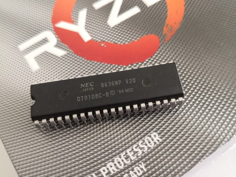
  • CPU: NEC V20, 8MHz (overclocked to 10MHz after some weeks)
  • Mainboard: No-Name 8088, fully populated with 640KB and 5 ISA slots
  • Video: No-Name Hercules compatible (to an amber 12″ screen)
  • Media: Seagate ST-225, glorious 20MB, MFM controller and a 360KB 5.25″ Floppy drive

It was fun hacking my way through Turbo-C/ASM, TSRs and such but even overclocked it was a sloth…

1990 – Affordable 32bit! And an option of UNIX…

About quitting my job at the computer store I traded my XT for a bare 80386 system on my way out. Bare because I had no money left for a case… and also because having a ‘proper SCSI’ solution was more important to me after seeing Interactive UNIX running at a friends system I planned to have that too, some fine day… so this “PC” was running lying naked on my desk. It consisted of

  • CPU: AMD 80386, 33MHz
  • Mainboard: No-Name 386, populated with 4MB and five 16-bit ISA slots
  • Video: No-Name Trident 8900, 512K (IIRC)
  • Media: A 5.25″, full-hight 170MB SCSI monster (I think it was Micropolis and already considered vintage – but cheap!) attached to a fancy (and very much loved) Adaptec 1542b – and a 1.4MB 3.5″ floppy of course.

It turned out that there was no way to get a proper UNIX for cheap – and it wasn’t planned to pursue this path any further…
(During these days in my view Apple and Acorn still were the things to come – it shows how wrong you can be)

1992 – Linux happened

Early 1992 I got wind of this Finnish guy and his ‘tuned MINIX’ – digging into the news further I was on fire, got myself a ~40 Floppy Distro (A Slackware clone from ‘Linux Support Team Erlangen’) and immediately understood, that a 386 and 4MB isn’t much if you want X11, too.

So I swapped my x86 again and got myself a 80486/33 which I originally bought as office workhorse for my first own company (which did not work out so well). Having doubled the RAM this also brought a speedy ET4000 with a whopping 1MB video-RAM making X11 possible.

  • CPU: Intel 80486, 33MHz
  • Mainboard: No-Name 486, populated with 8MB and five 16-bit ISA slots
  • Video: ET4000, 1MB
  • Media: Replaced the lame AT-BUS by my SCSI rig from above.

1994 – Going serious

Finally I was in UNIX heaven… and using a UNIX system (Linux in this case) you never have a sufficiently fast system. It became clear that my 33MHz 486 hit its limits and even my dear AHA1542B felt slow looking at this brand new PCI-Bus everybody was going crazy about. So I skipped EISA and looked for the best solution.
Attending the release show [German] of the brand new Intel Pentium at Cebit ’93 it became clear that I’ll ignore that an go for an Am5x86 and the best board you can get: The ASUS PCI/I-486SP3G

  • CPU: AMD 5×86, 133MHz
  • Mainboard: Asus 468SP3G with 16MB, four 16-bit ISA and 3 PCI slots
  • Video:ET4000  (replaced in 1995 by an S3 Trio64, 2MB)
  • Media: Onboard NCR53c810 SCSI driving a 3.5″ 200MB HD and 2x CD-ROM

1996 – Bad Ass mode

Compiling kernels and stuff like that squeezed the last inch of performance out of my trusty 5×86 (now running at 160MHz) it had to be something faster again… Having some cash at hand I decided to go “32bit and no way  back” and opted for the cool & huge Pentium PRO @ 200MHz which I got for a very good price (used, from an integrator evaluation site) before I even had a board for it.
After some research it had to be the bad-ass Tyan S1662D mainboard, featuring a 2nd socket to go dual CPU – how crazy it that!? A year later, that socket got populated and besides my Linux power-house (make -j2!) this box also rendered Cinema-4D movies like a maniac (I even was beta-tester for Maxxon).

  • CPU: 2x Intel Pentium Pro/200
  • Mainboard: Tyan S1662D with 32MB, tree 16-bit ISA and 5 PCI slots. Stuffed to 256MB later.
  • Video: S3 ViRGE/VX 2MB, replaced by later by a very much loved Nvidia Riva 128/4MB
  • Media: Symbios Logic 53C875 PCI SCSI controller driving a 3.5″ 500MB HD and 2x CD-ROM

1999 – Last x86 update for a long time

Finishing my studies I mainly used my beloved PowerMac 6100 for creative work, while my ‘Pro’ was Linux and render-box only.
I started a day-job in IT earning real money and had the chance of hosting my server – so the PPro became my first physical server hosting this very page (and others). So I needed to get into PC builds gain – even I can’t remember a real reason for this 😉
Intels Pentium-II easily outperformed my two PPros already and AMD did not convince me with their product line, so it became an PII @ 333MHz and an Asus P2B-F board which ran solid as a rock… but when my iMac G4 with OS X moved in, I got the perfect UNIX/BSD system I ever wanted and this little PCs fate was clear… it replaced the PPro Webserver. The PC-at-home time ended…

  • CPU: Intel Pentium II 333MHz
  • Mainboard: Asus P2B-F with 512MB, tree 16-bit ISA and 5 PCI slots
  • Video: AGP Riva TNT
  • Media: ATA became cheaper and faster than affordable SCSI. So this was the end of an era.

The Orphan

In 2012 I inherited my work PC when they closed office and I was pink slipped. Well, if it’s free… and a nice system it was: The Intel i7 2600K is still considered a decent CPU and was an animal back then. The Gigabyte z68x-ud3 mainboard neither is a bad choice (if you don’t need the beta UEFI BIOS) and this box made a strong gaming box with some casual VM and Hackintosh experiments… but beyond that, Macs-only it was from 2000 up to now.

  • CPU: Intel i7 2600K
  • Mainboard: Gigabyte z68x-ud3 with 16GB, still two classic PCI slots and some PCIe.
  • Video: Some AMD 6950 I think…
  • Media: SATA SSD and HD

One box to rule them all

Because my MacPro 3,1 (early2008) finally reached its limits – even rigged and modded to run Mojave (Incl. Metal graphics) just fine. Compared to its size and power consumption the performance doesn’t justify running it for longer. The i7 PC sitting next to it started to annoy me with its beta UEFI BIOS and it clearly started showing its age.
So this brought me to the decision to modernize while consolidating. Still owning a legal licence of MacOS (and some more Macs in the household) I will build a single machine, hosting MacOS and Windoze 10 using all the latest shebang – and going back to where my x86 heart is (if there’s something like that ;-)): AMD.
AMD is back. Big time. The Zen architecture really brought them back into the race and they caught Intel cold.
This means my one-an-only (recent, not vintage ;)) system will something along these lines:

  • CPU: AMD Ryzen 3600
  • Mainboard: Asrock b450 pro4 with 16GB, no classic PCI slots and about 4 PCIe with different lanes.
  • Video: AMD R9 280 RX570…
  • Media: M.2 SSD and still some HD for the archives.

Conclusion… for now.

Phew, this all came a long way. 31 years of building x86 PCs… and how things changed (as they did with my SPARC comparison):

Let’s compare the first and last CPU of the above list

Spec NEC V20 Ryzen 3600 factor
Max stock MHz 8 4200 33600
External Bus-width 8 64 8
Max addressable RAM in MB 1 32000 32000
Pins 40 1331 33.2
Manufacturing process 1200nm (less than half of Intels 8088) 7nm 171.42
Transistors 63.000 (double of an i8088) 9.900.000.000 (sum of chiplets and IOD) 157142.8
Cache 0 35.3 MB (all levels)

(more Cache than a 286 could even address)

Opcodes 154 About 1013 (incl. everything from MMX, SSEx to SGX/VMX/SMX) 6.5

That’s quite impressive, isn’t it? I’m still blown away by the number of instructions… ~1013! Holy Bat-Opcode! IIRC the 6502/10 had 56… and still isn’t considered pure RISC.

Intel EISA Chipset

This chipset started it all… it was the first EISA chipset produced and the one which riddled me the most. Mainly because I have two EISA boards behaving differently when it comes to expansion cards which were developed later (~1992-94) and so I suspected the Bus Controller to be the reason for all the hassle:

The Hauppauge 4860, an early EISA system and my Intel Professional Workstation (aka LP486, not yet documented on this page).
The first is using a 82350 chipset while the latter has a 82350DT. Where’s the difference? There’s no clear answer to this anywhere, so I had to do some lenghty, in-depth research.
Good that I do not only collect ancient cool hardware but also some documentation, e.g. the 2″ thick Intel “Peripheral Components” handbook from 1991…

Intel_Periph

Here’s my conclusion:

The ‘original’ 82350 Chipset -released May 1990- included just 2-3 chips: 82357, 82358(-33) and (optionally) 82352.
The 82350DT -released April 1991- consisted on 5-7 chips: 82357, 82358DT, 82359, 82351, 82352, 82353 (some of them used multiple times).
The difference between the non-DT and DT version of the 82358 seems to be the synchronous interface to the 82359 DRAM controller, which wasn’t available in the initial chipset.

Chip-by-chip round-up of the chipset:

The 82350DT EISA chip set contains 7 VLSI chips to build a complete EISA
system. It is built upon the 82350 EISA chip set utilizing the 82358DT EBC and
82357 ISP and then adds VLSI components:

  • 82359 DRAM controller.
  • 82353 Advanced Data Path,
  • and 82351 LIOE Local IO Peripheral

The picture below shows a 486 based system with 82350DT chip set.

illu

The host bus connects the CPU and the memory subsystem. Tlte peripheral bus (X-bus) is an 8-bit bus to support the motherboard IO functions: keyboard, floppy and the LIOE which integrates the parallel port; and support: extemal teal time clock und serial ports. The peripheral bus is a buffered version of the 8-bit ISA bus. The memory subsection operates independent of the CPU clock. This independence is accomplished through the use of 82359’s integrated programmable delay line and the  rogrammable state tracker(PST) function. The integrated programmable delay line is used to time precisely the DRAM cycle sequence to DRAM parameters. The PST resides cm the CPU module. Tite 82359/82353 reside on the motherboard. They are indifferent to the CPU/cache used. The PST converts processor cycles to a form acceptable to the 81359. This allows different CPU/ cache combinations to be connected to the same motherboard. Further, it translates CPU’s clock-dependent handshake to clock-less memory interface handshake.

Local I/O EISA Support Peripheral, lntel 82351

The 82351 supports or integrates all of the IO peripheral functions for a typical EISA system board with a minimum of external logic. lt integrates local I/O ddress decoder, EISA system configuration registers, two external serial I/O ontroller interfaces with four assignable interrupts generation, external EISA onfiguration RAM interface, parallel port interface, external floppy disk controller Interface, external keyboard (8×42) controller interface including interrupt generation, and external real time clock interface and EPROM or FLASH EPROM BIOS ROM interface. lt was available in a 132-pin PQFP (Plastic Quad Flat Pack) package.

EISA Bus Buffer (EBB), Intel 82352

The 82352 is a bus buffer IC for EISA bus system. Three 82352 chips are used in a 82350 EISA system. Only one 82352 chip is used in a 82350DT EISA system.
lt operates in three modes. ln Mode 0 it performs data latch and swap functions.
It allows swapping and assembly of  data between the host and EISA/ISA buses on a byte by byte basis. In Mode 1 it provides 1 buffered path between the host data bus and DRAM with parity generation/check. Mode 2 was reserved by Intel for future use (never happened). Mode 3 provides address latching function between the host and EISA/ISA buses. The 82352 was available in 120-pin quad flat pack (QFP).

Advanced Data Path, Intel 82353

The 82353 provides advanced data path in e 82350DT EISA bus system. Two 82353 chips are used in a 82350DT EISA bus system as showed in the graph. Each 82353 is designed as a 16-bit slice. Two 82353 chips can provide parallel interface to 32, 64 or 128- bit wide memory structures to a 32-bit host and system bus.
The 82353 provides optimal 486 burst performance. Each memory cycle enerated by the address controller chip causes 128 bits of memory data to be latched in two 82353 chips. Once data is latched, these 82353 chips mux the four dwords to the destination in one wait state. The 82350DT EISA bus has 128-bit memory bus. A typical burst is 128-bit wide. and a bus with the same width
allows to read the whole burst in one memory cycle. This provides a zero wait state burst at any frequency. The 82353 was available in a 164-pin PQFP package.

Integrated System Peripheral (ISP), Intel 82357

The 82357 contains DMA controllers, interrupt controllers and programmable 16-bit counter/timers. lt provides high-performance arbitration for CPU, EISA/ISA bus masters, DMA channels and refresh. It also provides logic for generation/control non-maskable interrupts. The DMA function is provided by two inbuit 82C37A DMA controllers. These DMA controllers are connected in cascade mode to provide seven independent programmable channels. The timing control for 8-, 16- and 32-bit DMA data transfer is provided. The data transfer rate is 33MB/sec. There are two 82C59A interrupt controllers in the 82357 chip, which provide 14 independent programmable channels for level or edge-triggered interrupts. The 82357 contains five 82C54 compatible programmable 16-bit timers/counters. lt was available in a 132-pin PQFP package.

EISA Bus Controller, Intel 82358DT

The 825358DT provides an interface between 386/486 CPU and EISA bus system.
It provides EISA/ISA bus cycle compatibility with the host(CPU) bus. The 82358DT is a part of intel 82350 and 82350DT chip set. It translates host(CPU) and 82359(DRAM controller) cycles to EISA/ISA bus cycles. lt supports 8-, 16- or 32-bit DMA cycles. lt also supports host and EISA/ISA refresh cycles. lt generates control signals for advanced data path(82353) and EISA bus buffer(82351). lt was available in a 132-pin PQFP package.

DRAM Controller, lntel 82359

The 82359 is a highly integrated advanced memory controller. lt supports 386 and 486 microprocessors. Its operation is independent of speed and type of the CPU. It allows a system designer to implement a variety of CPU/cache combinations. It provides address control, refresh generation and critical DRAM timing generation. In conjunction with two advanced data path devices (82353), it acts as a highly integrated 32-bit dual ported memory controller. Its two ports (or address gateways) to main memory are: one exclusively for the host and one exclusively for EISA. This configuration of ports permits CPU activity to be isolated from EISA bus activity. It controls up to 256MB of motherboard DRAM. It supports 32-, 64- or 128-bit wide memory configurations. lt was available in a 196-pin PQFP package.

Bus Master Interface Controller, Intel 82355

The 82355 is used in an EISA add-in card (expansion board) – thus rarely found on mainboards.
It supports 16- and 32-bit burst transfers at maximum data transfer rate of 33MB/s. It also supports 32-bit non-burst and mismatched data size transfers. It automatically handles misaligned double-word data transfer with no performance penalty. It has two independent data transfer channels with 24-byte FIFOs. Expansion board timing and EISA timing operate asynchronously. The 82355 supports 32-bit EISA addressability (4GB). It integrates three interfaces:
EISA, local CPU and transfer buffer. It supports automatic handling of complete EISA bus master protocol. This includes EISA arbitration/preemption, cycle timing and execution, byte alignment, etc. Further, the 82355 supports local data transfer protocol similar to traditional DMA. It was available in a 132-pin JEDEC PQFP package.

The EISA Bus

Actually I have no idea why this subject caught my interest so well.
During the hey-days of the EISA bus I wasn’t interested at all, thought that’s something which will never take off and was intended for servers only. I happily stuck to clumsy ISA and sat there until PCI was affordable (ASUS SP3G anyone?).

Now, fiddling with all those exotic cool mainboards, EISA crosses my path all the time. The way EISA is configured, the somewhat cumbersome use of cf.exe (ECU – EISA Configuration Utility) tool drew my interest… maybe because it has the scent of manliness 😉

In my humble opinion, EISA was a crutch, but it layed some basics for the next 10 years:

  • It defined (as a by-product) a standard for the ISA bus, which was all chaotic before
  • It forced Big-Blue (IBM) to think over their Microchannel licensing
  • It was a test-bed for how do things right… later known as PCI

That said, it is the fun twilight-zone between ISA’s direct access “do what you like” and PCI’s “you touch – you die” approach. Where else do you have 32-bit speed and can still change bits manually with DOS’ debug?