Category Archives: Transputer Hardware

Transputer Hardware

AVM B1 hacking

Intro

Transputers were created to control everything. They were not just CPUs… they could do the video output, control interfaces or even storage devices. So no wonder there were ISDN and SCSI controllers available using transputers.

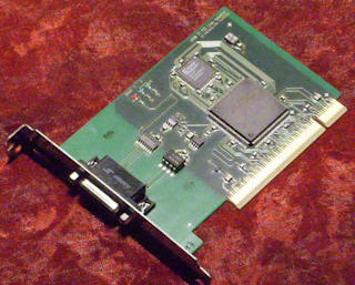
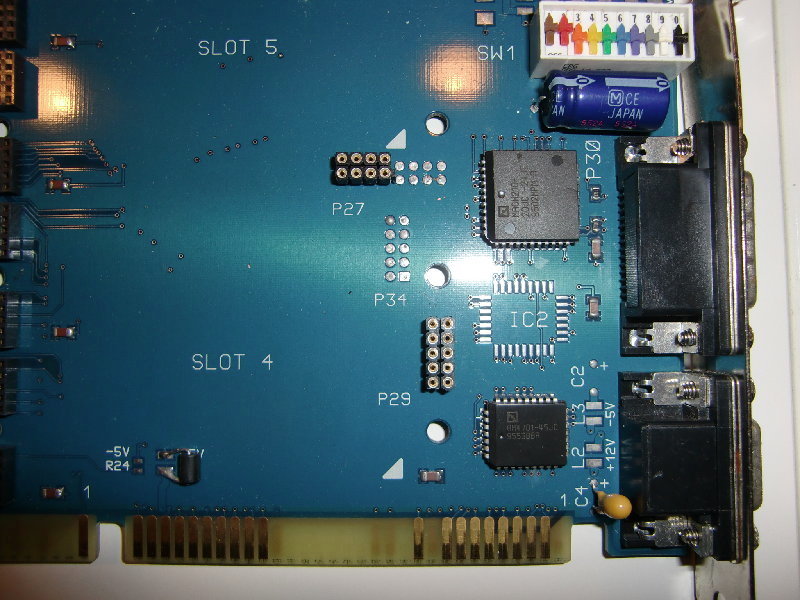
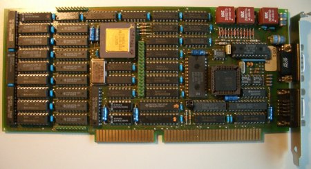
One of those transputer-sporting controllers was the AVM B1 active ISDN card. Back in the PC-AT days, handling the ISDN protocol and traffic could easily bring down your super-cool 80386/25 without a problem, especially if this machine should also fulfill server tasks.
So active (vs. passive) ISDN cards were the cure to that issue. They featured a CPU of their own with some RAM to buffer the data coming in at the maximum ultra-fast rate of 128kbps 😉

In case of the the AVM B1 the CPU was a transputer (T400) and that had reign over a whopping 1MB of RAM! When the card was installed and the DOS driver booted, it actually loaded the transputer code onto the card like any normal transputer card would be fed with code – behaving like an Inmos B004 card and even using the same port addresses.
So in fact, the AVM B1 is a transputer card featuring an ISDN-part connected to one of the transputers links.

Using the usual tools for finding and checking a B004 compatible card shows this

> ispy | mtest Using 150 ispy 3.21 | mtest 3.21
# Part rate Link# [ Link0 Link1 Link2 Link3 ] RAM,cycle
0 T400b-20 43k 0 [ HOST ... ... ... ] 2K,1 1022K,6.

Weapon of choice


Ok, cool – so where do I get this card?

Well, AVM is still very alive-and-kicking but they’re not building these cards (using transputers) anymore… even if they wanted to, Inmos/SGS killed the transputer back in 1993. So eBay is your friend.

Anything to watch out for?

Yes! AVM build(s) 4 major versions of the B1: V1 to V4.
V1.x – Available as ISA and MCA version. The perfect choice! Everything important is socketed, no SMD parts.
V2.x – ISA version only. CPU & RAM is SMD. Ready to play with but not much to mod.
V3.x – ISA & PCI version. Updated version, same features like V2.x
V4.x – PCI version only. No transputer anymore. “StrongT” Controller… might hint towards a StrongARM based thingy.

Again: If you want to do all the hacks described here you have to get a Version 1.x card!

Enhance it! This is the easy part…

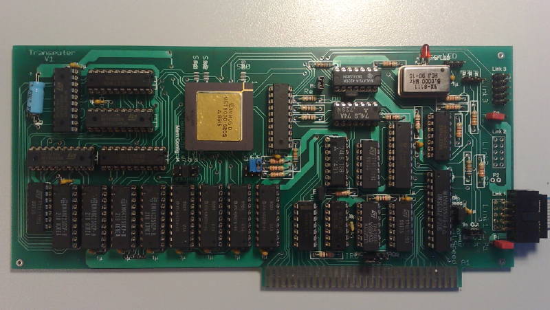
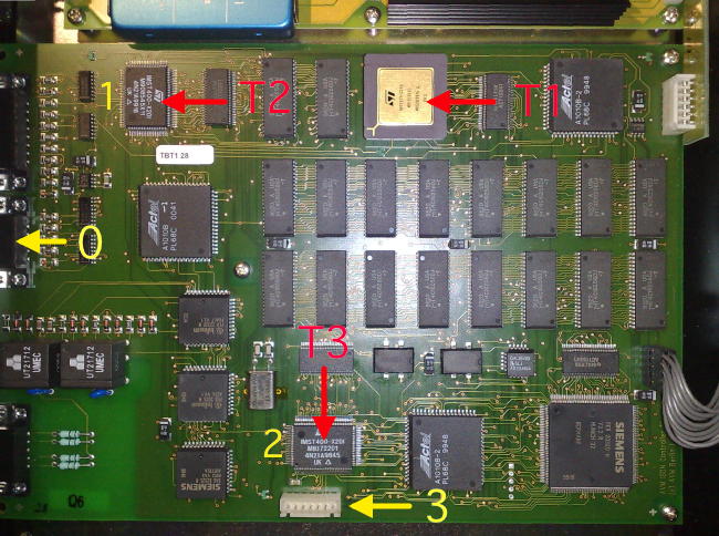
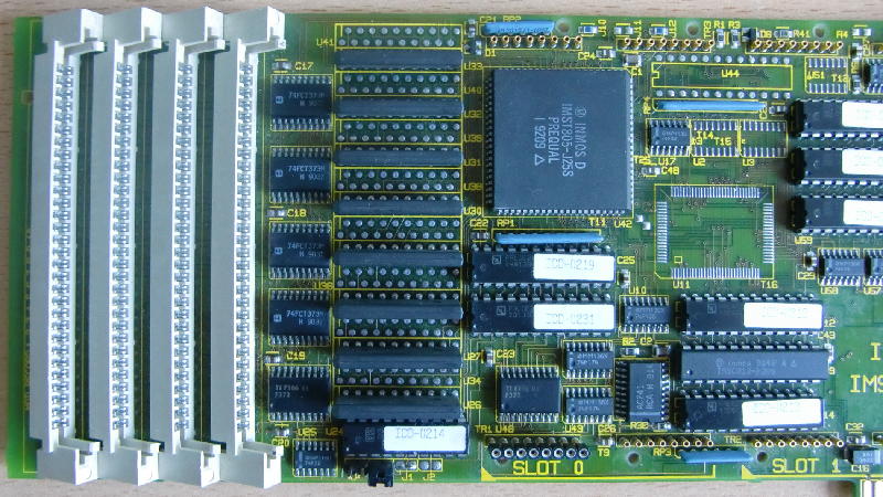
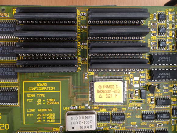
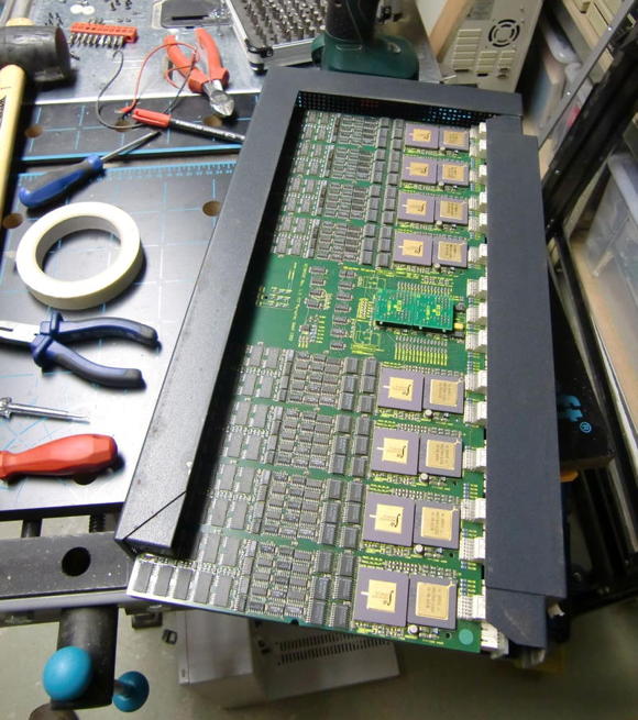
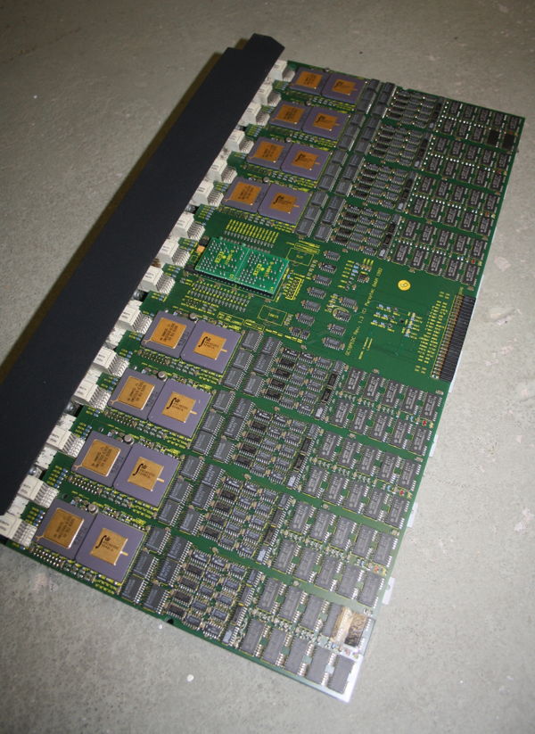
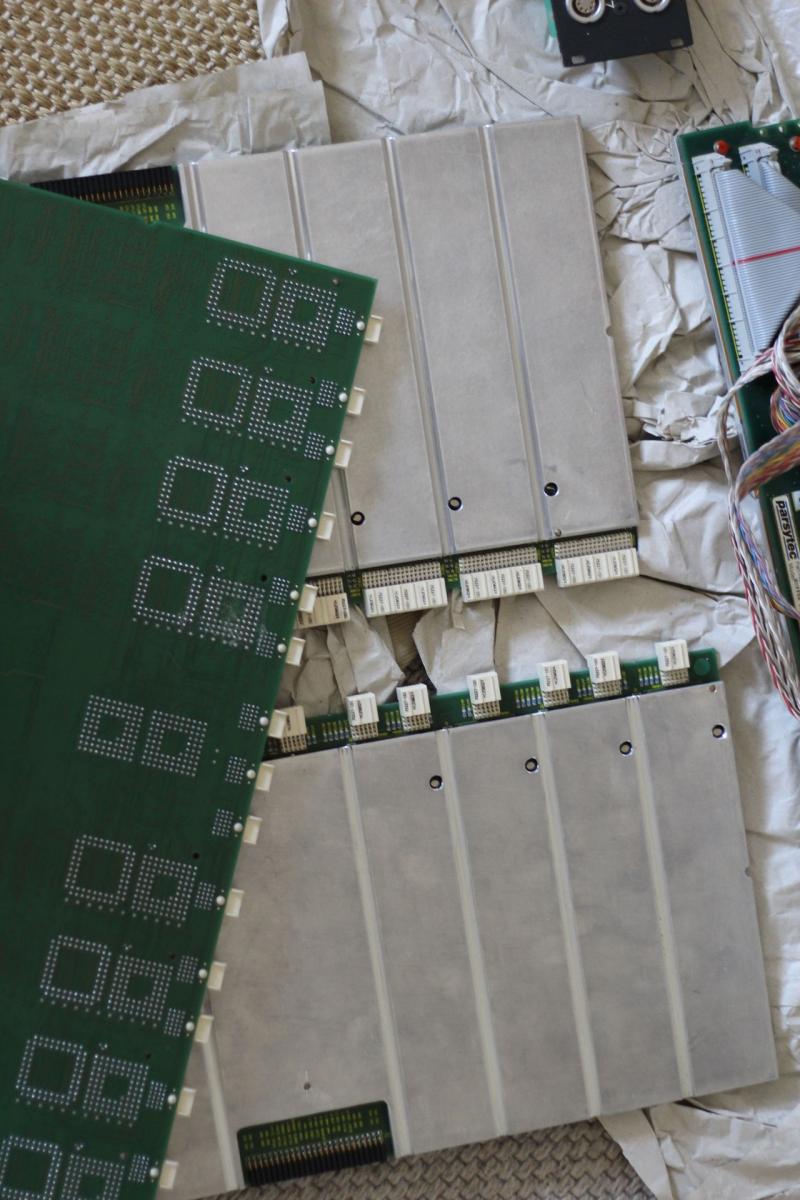
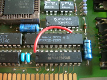
Ok, so I assume you fought hard to get a V1.x B1… it should look like this:
(If you acquired an V2.0 card which is smaller and has lots of SMD parts on it, check out Jonathan Schillings page (German), who did all the mods described here with a V2.0 card)

TheBeast

If you have your card in front of you, you might spot some differences. These are the first two and most obvious “mods”:

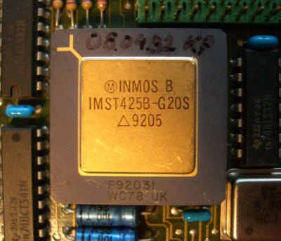
  • Change the T400 CPU (e.g. to a T425 or even T800)
  • Add more RAM

The T400 is OK to begin playing with this card, but it only offers 2K internal RAM (vs. 4k in the T425/800) as well as it has only 2 links: One connected to the C012 (and this going to the ISA interface) and one is available. I was under the impression, that AVM might use the other link to interface to the ISDN part, but that seems to be memory-mapped.
Changing to a T425 gives you more internal RAM (=speed) and the possibility to use 3 external links to talk to more connected transputers.
A T800 would be the top-of-the-hill, featuring an FPU which will speed up your Mandelbrot tremendously.

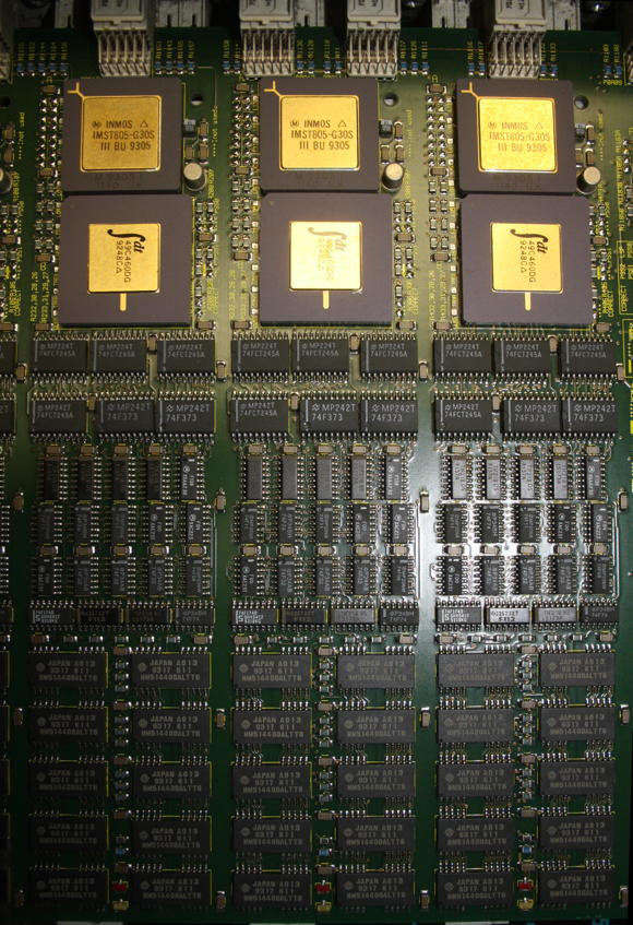
So here’s my T425 which replaced the stock T400. At about 8-10 Euros you should be able to get one at ePay…

CPUChanged

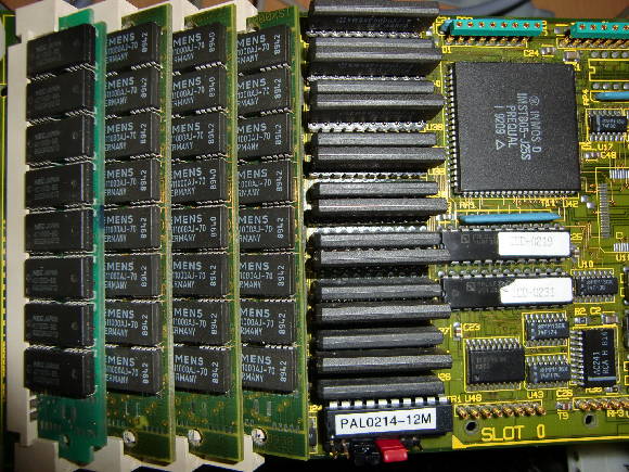
Next up, the RAM. Albeit the standard 1MB are plenty enough for nearly all fooling-around you might plan, there’s another Axel-Law to be followed: “If there’s an empty socket, fill it!”.
Also if you’re going serious and think about running the Helios OS on this card, you’ll better have 2MB!
You need to get eight 256Kx4 chips – they’re pretty common. They should be faster than 100ns… you’ll read later why.

RAMAdded

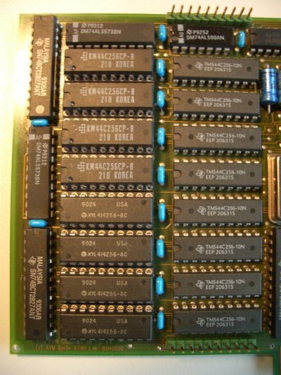
The eagle-eyed reader might spot the different makers of the RAM chips. That’s because I’ve salvaged 2 old ISA-VGA cards (each 512k) for the chips. All are spec’ed at 80ns.

Another run of the transputer find/check-tools now shows this

> ispy | mtest

Using 150 ispy 3.21 | mtest 3.21
# Part rate Link# [ Link0 Link1 Link2 Link3 ] RAM,cycle
0 T425b-20 43k 0 [ HOST ... ... ... ] 4K,1 2044K,6.

Not bad, huh? But there’s room for improvement… the RAM is accessed extremely slow, set to 6 clock cycles which is very conservative, even for 100ns RAM parts.

Faster RAM – The not-so-easy part…

Ok, up to here it was a piece of cake, wasn’t it? Now we’re switching to hard-core mode 😉

RAM-Access speed-up

For this you’ll need

  • Some soldering know-how – and a solder-iron of course
  • A calm hand
  • A continuity-tester or multimeter
  • A thin cutter
  • the pinout of a transputer (available in the data sheet (PDF))

As said before, the RAM access is very slow. It’s set to 6 clock cycles which is recommended for 150ns parts even at 20MHz. So for a start we should be safe going down to 5 cycles even with the standard 100ns RAM chips…
The RAM is controlled by the transputer itself – something the Intel-World introduced with the AMD Opteron years later!

When booting, the transputer checks how his “MemConfig” pin (position C8) is connected to the MemAD[3-7] pins to determine the RAM speed. The AVM B1 has its “MemConfig” connected to MemAD7 (position K10) which we want to change to MemAD6 (J8) in the first step.
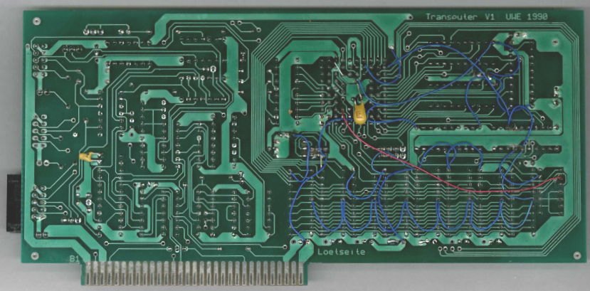
The AVM B1 is a 4-Layer card and unfortunately the wire connecting those two pins is running in the 2nd layer from the back.

To find the trace we have to cut, hold the card in front of you looking at the component-side – like the first picture on this page. Now flip it vertically. You’re looking at the solder-side, the external connectors pointing to the left.
A closer look at the transputer pins shows you where to cut and the wire connecting “MemConfig” with “MemAD6” – Pin A1 is in the upper left corner, counting down[123456789,10], letters right [ABCDEFGHJK]!

RamSpeedMod

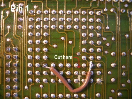
The cutting is a delicate thing to do. So be very careful not to cut too deep. I did it by cutting carefully once or twice and then checking with a continuity-tester if MemConfig and MemAD7 are still connected. Repeat until the connection is broken.
If everything went fine solder a wire between the two pins. Don’t make the wire too short, so we can change/move it anytime later. Another test shows this now:

Using 150 ispy 3.23 | mtest 3.22
# Part rate Link# [ Link0 Link1 Link2 Link3 ] RAM,cycle
0 T425b-20 43k 0 [ HOST ... ... ... ] 4K,1 2044K,5.

Yay! RAM’s accessed a bit faster now.

If that works and you’re like me (squeezing out the last drip of everything) you can try connecting to MemAD5 (J9). It worked for me.

Faster Link Speed – Not for the fearsome!

The next thing being rather sub-optimal is the link-speed… 43k/s is dran slow.

Using 150 ispy 3.23 | mtest 3.22
# Part rate Link# [ Link0 Link1 Link2 Link3 ] RAM,cycle
0 T425b-20 43k 0 [ HOST ... ... ... ] 4K,1 2044K,5.

That’s because it’s locked to 10Mbit/s by AVMs design even 20Mbit/s would be possible. Again, the transputer gets its configuration during boot-time via special pins. In this case LinkSpecial(A2), Link0Special(B4) and Link123Special(A4).

Not a big deal, but in case of the AVM B1 it’s not solvable by simply putting those pins high or low. That damn card is -again- a multilayer card and one of those layers is a ground-layer. No way in cutting a trace here.
The only solution is an in-between socket… a calm hand and pincers >:-)

socket_top
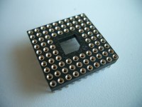
Ok, first you have to get another 84-pin socket. It’s not so easy anymore to find those… luckly, I had one spare collecting dust.

You might find an alternative socket meant for a Motorola 68881/2 FPU – but make sure it also has the inner pin-rows connected. Normally the 68881/2 has 8 pins less!
Another possibillity would be making a socket by glueing 10×1 pin-rows together. Not pretty but should do the job.

For the second step, you’ll need a caliper and (again) the transputer pinout. Orientate the socket so that pin-1 is in the upper left corner (the picture above shows this by the angled-corner in the center of the socket).
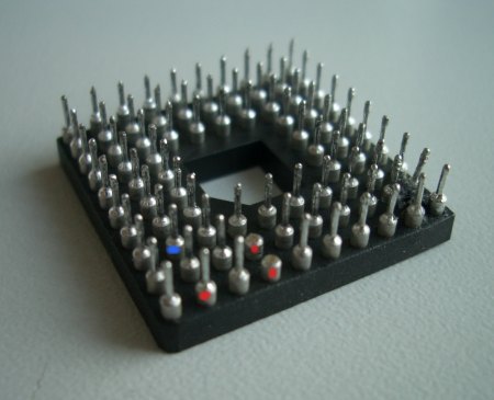
Now identify the pins LinkSpecial(A2), Link123Special(A4) and Link0Special(B4) as well as one VCC-Pin of your choice (I went for C2). We need to connect those 4 pins, pulling all Link[n]Specials high… which gives us 20Mbit/s link speed!

Note: If you plan to use the B1’s external links, you might consider not to change the external link-speed – read more about this in the next chapter.
In this case do not change Link123Special(A4).

So carefully cut the thin part of the pins A2, A4 (see note above!) and B4. Use a rasp/file to shorten the pin down to the thicker base (so the remaining part can’t connect to the original socket).
This is how it looks already having A4 & B4 cut off, A2’s still due (all marked red) – Do not cut the VCC-pin (C2, marked blue)! :

socket_pins_cut

When everything’s nicely cut, use a wire to connect them together – it’s a bit tricky to solder between the pins, so use a fine tip.
When you’re done, the socket should look like this:

socket_pins_solder

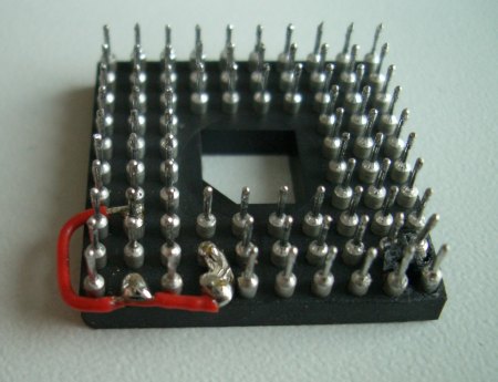
Now double check the modded pins for shorts to their neighbours!! Not doing so might kill your transputer/card!!

Cool! Were half done. For the third step we need to adjust the other side of the link accordingly. “The other side” is the Inmos C012 link-adaptor sitting in the lower right corner of the card -close to the ISA connector- labeled “IMSC012-P20S”.
Identify pin-15 and use a thin caliper to cut its leg as close to the board as space allows it. Bend the remaining leg up and check that there’s no connection to the card anymore.
Now solder a wire going from pin-15 to some VCC source. I’ve chosen Pin-20 of the 74ALS245 next to the C012. This is how it looks on my card:

C012_mod

[Note: Make your wire long enough so you can reach some GND pin with it. So you can reverse the mod easily.]

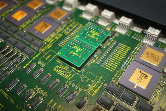
We’re nearly there! For the forth and last step, plug your transputer into your in-between socket and the whole thing into the original socket on the card like this:

socket_seatedt

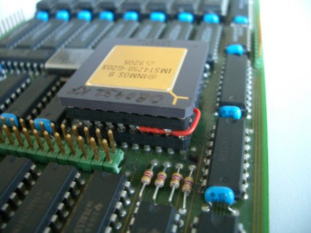
Done! If everything was done right the usual tools should give you some serious number (well, it’s still far away from the theoretical 1.7Mbit/s, but at least 8.8 times faster than before):

Using 150 ispy 3.23 | mtest 3.22
# Part rate Link# [ Link0 Link1 Link2 Link3 ] RAM,cycle
0 T425b-20 378k 0 [ HOST ... ... ... ] 4K,1 2044K,5.

378k/s is faster than my crappy Gerlach-card (@239k), even the AVM is also just using 8 data-lines of the ISA bus (being a 16-bit card it only uses 4 lines from the AT bus… for IRQs 10-13).

So… what else can be done?

The external Connector

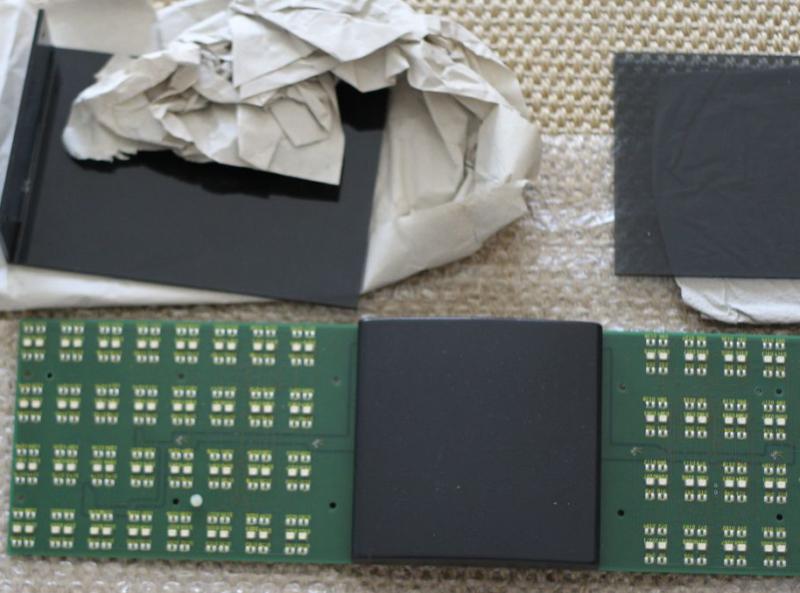
The AVM B1 v1.x cards feature a mysterious (green) connector:

ExpansionPins

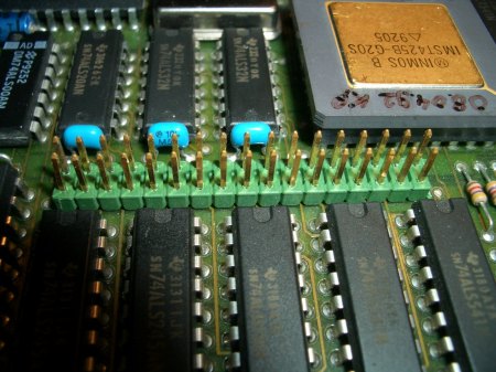
It’s undocumented… up to now 😉 I just started tracing all the connections, but I’m happy to say that even AVM did everything possible to cripple the B1 card, they did not dumb it down completely:

Link[123] & Reset (not inverted!) are brought to the outside!! Error and Analyse are hold to GND, though.

Note: That said, AVM wouldn’t been AVM if they didn’t save a dime… the external links are buffered (at least) by a comparably slow 74BCT541 octal buffer.
This offers a signal propagation delay of ~9ns while INMOS recommended to use “F” type buffers, which offer a speed of about 3-4ns. So 20mbps are too fast for this chip. 10mbps should work though.

Here are my findings so far: [work in progress]

I started counting pins from the transputer, zig-zag, downwards. Interesting things coloured green.

1 2
o o
reset o o
o o
o o
o o
o o
PEB2070
o o (to its pin 10)
Link3Out o o
Link2Out o o
Link1Out o o
Link3In o o
Link2In o o
Link1In o o
GND o o
o o
GND o o
o o
33  34

Das Transputerbuch

There was one major german book about transputers called “Das Transputerbuch”, written by Uwe Gerlach (ISBN 3-87791-019-X).DasTransputerbuch
What made this book special was that it included an unpopulated 8-bit ISA card for a transputer and 1MB RAM, fully B004 compatible.
Additionally, there were schematics provided to build a host-adapter for several homecomputers of that time (C64, Apple II, ATARI ST and Commodore Amiga).

I was able to get one book off ePay which was still includung the printed circut board and a 360k floppy containing some sample sources and a rudimentary assembler.
So I’ve polpulated it, found some mistakes Gerlach made and made it somehow run.

This is how the card looks

Gerlach

It’s design is pretty simple – at least compared to the efforts been taken with the i860 cards on this page. The simple design is also because the Transputer has nearly everything included… so what you see is:

  • The right half is the ISA-bus and link interface. The rightmost and longest IC is a C012 connecting the 8-Bit ISA bus to link0 of the Transputer. Everything else are buffers & drivers.
  • The left half is -besides the Transputer itself- just 1MB RAM and some address-logic. The card would also work without having this side populated using the internal 2 or 4k of the Transputer.

C’est ca. As said, prety simple.

The mentioned bugs of the card are:

  1. The orientation of U11 and U12 are wrong on the print on the PCB and in the book, check the photo for them.
  2. There are no holes for the capacitor near to U28, you will have to solder it to the corresponding pins on the back of the PCB.
  3. The crystal oscillator U12 has its pin-1 not-connected, but it is connected to ground on the board. My crystal oscillator didn’t generate a clock signal, when pin 1 was connected to GND, although it normally shouldn’t matter.

Still, there was a persistent problem with the external 1MB RAM. It was detected by mtest but depending on the Transputer-type used and some randomness, it never was checked as being ok.
Replacing  some capacitors and strengthening some ground traces helped but it’s still not clear what the real reason was.

Here’s the back of the card – looking like a snake-pit now 😉

GerlachBackMod

Hacking the AVM T1

AVMT1Press

It was inevitable… the biggest system AVM built was the “T1”, a 30 channel ISDN controller in a sleek 1U 19 inch case of which nothing more than the above marketing picture seems to exist.
One fine day I had to had one – and today is the day!

I was able to find a AVM T1 on ePay which was not very well advertised so I had no “professional competition”. Even I didn’t spent a fortune it was a bit of gambling because I didn’t knew what to expect.
Besides AVMs own T1 PDF manual there’s next to nothing available in the Web – So this section is yet another WWW-exclusive brought to you by geekdot.com 😉 (Ok since 2009 others discovered this page and also this cheap entry into the wonderful world of multi Transputing)
Still, the docs said “a Transputer network with 9MB RAM” so I couldn’t go completely wrong. That said, I was expecting SMD T400s at AVMs usual sluggish speed…

First look

When the box arrived first thing was getting out good ol’ screwdriver and open the case…

AVMT1open

…and I was very surprised:

  1. A socketed T425 – so that’s another easy upgrade then.
  2. An external power supply (48V)! That’s strange but also neat – no noise and next to no heat in the case itself
  3. Also, the board is very small…  lot’s of room left in the case.

That’s done by intention as you could buy the T1-B, where “B” stands for the “Booster Board”, yet another board with 4 more Transputers and another 8MB of RAM giving a total of 7 Transputers and 17 Megs of memory. Quite a setup for just an ISDN controller.

Sniffing around

Ok, this beast has to do something better than handling 30 boring B-Channels… Mandelbrot for example 😉 So let’s see how this thing is/was supposed to speak to the outside world.

The manual is talking about an ISA or PCI controller-card which will be connected to a 9-pin Sub-D connector. Having a closer look to the mainboard where that connector is seated I discovered some other old friends: AM26C31 and AM26C32.
Aaaaalrighty, RS422 time… that’s the same way my Tower of Power is transmitting its data. So I can use my TTL-to-RS422-converter I’ve built for the Gerlach card.

Out goes the multimeter and after a while I figured out the the traces on the board. For a better understanding, here’s the “map”:

AVMT1Board

Marked by the red arrows are the three Transputers:  T1, a T425-25, is the “application processor” while T2 and T3 are more simple T400-20 handling the ISDN subsystem.

The yellow arrows mark the four links of the T425 – which is probably the reason why AVM used a 425 vs. their usual T400: this time they really needed 4 links.
Link0 is connected to the 9-pin sub-D connector (via the RS-422 transmitters/receiver) for interfacing to the PC.
Link1 and Link2 are directly connected to the T400s.
Link3 goes to the connector on the lower edge of the board. I bet this is where the “booster board” would be connected… not a hard bet, I admit.

The pinout for the 9-pin sub-D connector (female) is:

 1 Link0-IN -
 2 N/C
 3 Reset-IN +
 4 N/C
 5 Link0-OUT +
 6 Link0-IN +
 7 Reset-IN -
 8 GND
 9 Link0-OUT -

As Link0-IN and Reset-IN are routed through two separate 26c32 I assume there might be more differential signals available. If time allows I’ll dig deeper on this matter.

Do something Gromit!

Well then… a cable was built in a couple of minutes – some cursing and swearing about the differential polarity and then the exciting moment came: Let’s see if it’s really so easy again!

It is! And here’s the ispy output for the T1 (connected to the “Gerlach card”):

Using 150 ispy 3.23 | mtest 3.22
# Part rate Link# [  Link0  Link1  Link2  Link3 ] RAM,cycle
0 T800d-25 288k 0 [   HOST    …    …    1:0 ] 4K,1 1024K,3;
1 T425c-20 1.6M 0 [    0:3    2:0    3:0    … ] 4K,1 4092K,3.
2 T400c-20 1.7M 0 [    1:1    …    …    … ] 2K,1 1022K,3.
3 T400c-20 1.8M 0 [    1:2    …    …    … ] 2K,1 4094K,3.

Some remarks about this:

  • 9 MB is true. The “application processor” (T1) got 4MB while the two T400s got 1 (T2) and 4 MB (T3, obviously connected to the SIEMENS Munich32 Über-ISDN controller).
  • While the built-in T425 is spec’ed for 25Mhz it’s just running at 20MHz… what a waste of bang… and what an opportunity for improvement :->
  • The linkspeed is at maximum… which one would expect with directly connected links. But with AVM you’ll never know 😉
  • The RAM-speed is pretty good (compared to what they did to the B1) – even they just used 70ns RAM.

Next up: Having fun with Mandelbrot! Having just T4xx Transputers it can only use the integer algorithms (i.e. no floating point) but who cares for a quick start?!

It’s working and showed another nice gadget: LEDs! Each Transputer has a tiny SMD-LED connected to it’s Link-Out.
So having the T1 underneath the table I have quite a nice light-show while the three are working their a** off 😉

If you happen to have no access to a RS422 converter: Never say die!
Like said above, there’s still Link3 available – normally meant for the booster-board – and it’s pure TTL. All you need is a somewhat non-standard plug to this connector. Be creative but don’t forget that unbuffered link connections only allow a distance of a couple of inches/centimeters!

The pin-out (so far) is, counting from left to right:

 1 - 5V VCC
 2 - T1 Link3 OUT
 3 - T1 Link3 IN
 4 - RESET
 5 - T3 Link1 OUT
 6 - T3 Link1 IN
 7 - GND

[UPDATE 11/14/10] Again, with some ePay-Luck I got another T1… and it again was some kind of lottery… and I had luck! This time it’s a T1-B!! This means, the “booster board” is installed. So opening the case, it looks like this. On the right the normal T1-board, to the left, “da mighty booster board” 😉 I’ll call it “BB” from here…T1-Booster-Full

As expected, it’s connected via Link-3 of the T1 Board. On the lower edge of the picture you can spot the power-supply “module”. It’s longer than in the T1 configuration and provides 3.3V/GND to the BB, i.e. the BB is 3.3v only!!

Here’s the BB alone:

T1-Booster-Board

All in all the BB is more modern than the T1-board. Very suspicious are the JTAG connector on the lower left having its lines connected to a EEPROM (AT28V256, right edge of the BB board, above the row of RAMs). Further up, left to the CPU nearby is a pad with the lable “Boot from ROM/Link”. I wonder what the default is and what’s inside that EEPROM – will investigate later.

Most importantly the BB board features 4 ST20450 processors, which aren’t INMOS products anymore. They were designed by ST after they bought INMOS. For short, the ST20450 is a T425 on steroids. More on-chip RAM (16K), higher clocking (40MHz) and some more instructions.
Each ST20450 has its own 2MB of RAM and a GAL handling the memory etc.. Here’s a close-up of a single ST20450 “module”:

T1-Booster-1of4

Mind the careful markings/labels on the board. The CPUs are numbered (“Processor 3”) and there are pads for Links etc.

Finally, I currently have no tools to check/use ST20450 processors. ispy finds the Transputers on the T1 board but freaks-out when it pings the ST20s.

Here’s another new addition: A picture of the official T1-PCI interface. It contains a PCI-controller (the big IC) and a XILINX FPGA… probably containing a synthesized C011.

T1_Interface

UPDATE:

Jonathan Schilling also plays played around with an AVM T1 on his page including the original ISA controller card… and he‘s making made very good progress!
[2015, Jonathan quit ‘the scene’ and handed over all his equipment… further on, it seems in 2020 he closed his pages]

Another UPDATE [2017]:

Just got another T1 off ePay… surprisingly it contained yet another board-design. I’ll call it the “non-booster layout“. This board has no connectors for the booster-board and missing the regulator below the DC/DC converter – no need for 3.3V.

TODO: 

  • Change the T425
  • Make the 30 front-panel LEDs blink
  • Figure out for what the female 15pin sub-d connector is good for (not mentioned in the manual)

Here’s how to access the LEDs at the front – thanks to Michael Brüstles research:

typedef unsigned long int u32;

/*
 *  addr XXXX-XXXX-X111-XXXX-XXXX-XXXX-XXXA-AA00
 *    
 *  wr                               0-01    __ EN __ __-__ __ __ SY
 *  wr                               0-10    08 07 06 05-04 03 02 01
 *  wr                               0-11    16 15 14 13-12 11 10 09
 *  wr                               1-00    24 23 22 21-20 19 18 17
 *  wr                               1-01    SC ST 30 29-28 27 26 25
 *
 *  rd                               0-01    readable ... content unknown
 */

int main( void ) {

    u32 *p = (u32*)0x80700000UL;

    p[ 1 ] = 0x40;  /* enable all leds 0x40 & Sync 0x01 */
    p[ 2 ] = 0x05;  /* Led01-Led08 */
    p[ 3 ] = 0x00;  /* Led09-Led16 */
    p[ 4 ] = 0x3F;  /* Led17-Led24 */
    p[ 5 ] = 0x92;  /* Led25-Led30, System, S-channel */

    return 0;
}

Caplin Cybernetics i860/Transputer cards

Caplin Cybernetics (just Caplin for short) was one of those many UK based (London to be exact) companies building Transputer based high-performance systems. Caplin seemed to be specifically concentrating on providing Transputer technology for DEC systems, namely VAXen.

As of now, I do not know much more about Caplin, but I know there are still some former employees around and I’d be happy to learn more about the company as well as the systems I’m going to describe further down.

By a lucky indecent I got my little greedy hands onto 2 different Caplin systems. Both connecting Transputer (networks) to a mighty Intel 80860XP.
While these boards have i860’s on them I’ve put them into this Transputer category, as they were meant as math accelerator for Transputer networks, not the other way round like the DSM860 boards, which used Transputers mainly for networking.

I don’t have any documentation for those boards but I hope to get them working as soon I figured out how to connect to the Transputers, find out more about the memory-mapping and found a way how to read those damn Bipolar-PROMs.

That said, from here everything is just wild speculation, assumption and finger-in-the-air-guessing – If you know more/better: Let me know please!

I’m specifically looking for the document called “Caplin XPR Series Technical Overview”. If you still have a copy or you do know somebody who might: I’d be very happy to hear from you!

HXI860

The HXI860 seems to be the earlier implementation of a Transputer-to-i860 board. It is a quite late i860 implementation though, featuring the first incarnation of the i860, the 860XR, predecessor  of the 860XP.

A picture says more than a 1000 words: The HXI860 in full view

HXI860-total

Let’s start with the left side of the board. The picture is a bit blurry (sorry) but it’s enough to identify what I’m going to talk about:

HXI860-upper

Starting on the left there are many blue 2-row pin connectors. This seems like a job for long winter evenings to find out which pin is connecting to what.
Then there are the 3 “golden boys” next to the connectors: From top down those are 1 T800-25 and two C004 linkswitches. Above the T800 there’s 4MB for his own use.
Then there are two FPGAs, one with the AT&T logo (ATT3020) and one more familiar XILINX XC2064, both getting their programming from an Xilinx 1736A PROM.
In the top-right corner the heavy-wight-champion i860XR (40MHz) surrounded by lots of buffers and GALs. The long DIP ICs on the right edge are IDT73210 octal transceivers with parity checking.
Rightmost are the connectors to the DEC Q-Bus… luckily only power & GND are taken from there, so you don’t necessarily need a VAX to use the board.

The right side of the board looks like this:

HXI860-lower

Ignoring the lurking C004 and Xilinx CPLD the leftmost black square IC is an T222C-17 which most likely controls the initial C004 configuration. He gets his code from two ICT 27CX642 which are quite strange devices: Made like CMOS EPROMS they use differential memory cell techniques to provide bipolar-prom speed. No idea how I will be able to read them out with my standard EPROM programmer.
Also, there’s a “6bit” dip-switch next to the T222 which I was told will be used to configure the link routing… let’s see what I will figure out by try’n’error.
The other four square ICs are 2Kx16 dual-ported RAMs (IDT7133). Four of them makes 64bit… well, that the i860 memory bus interface.
Last but not least there’s a long DIP IC above the DP-RAM… it’s an C012 Transputer link-adapter. So one Transputer link must be connected here, converted into 8-bit parallel. Could it be that they connected the 64-Bit RAM of the i860 via a transputer-link? (shudder)
Ok, and obviously there are 8 SIMM slots for i860 RAM… parity RAM required.

XPR201

This much bigger board seems to be the successor to the HXI860 and I was told it was the fastest i860 board Intel ever tested. Also this seems to be a prototype and was never officially sold.
It now features a 50MHz i860XP (fastest i860 available), two instead of one T800 but no C004 at all. Also the communication between the Transputer(s) and the i860 seems to be fully memory-mapped and no C012 is involved.

Here’s the full-view:

XPR201-total

Let’s go into detail… the “Transputer side” for a start:

XPR201-T800side

The connector at the top-right edge is yet of unknown type.
Below this, there are 2 T805-25, each having 4MB of RAM. Two AM27S33 4Kx4 bipolar PROMs (flanking the RAM to each side) seem to offer the 4K boot-code.
This board, too, has a 6bit dip-switch. Again, no idea yet what it does.

The most space in this picture is used by the much more sophisticated i860-to-Transputer interface, which is so complicated that it needs a diagram for itself (Thanks to Mike B. for beautifying this!):

XPR201

Eight(!) 4Kx16 IDT7024 dual-ported SRAMs are used to convert the i860’s 64bit bus to the Transputer 32bit bus – most likely they’re part of the “DMA engine”, too.

For doing this you normally only need 4 of them, but as you can see on the above diagram, Caplin chose to use the two T800 independently, so each Transputer has his own 16k SRAM directly connected to the i860.
Then, each Transputer is also connected to a 1MB VRAM bank (consisting of eight HM538123 having 128K word x8 DRAM and 256-word x8 Serial RAM). I was told the serial-side is connected to the Transputer, the parallel-side to the i860. Behind the VRAM is the “DMA engine” most likely the array of XILINX FPGAs you can see on the upper edge of the picture below.

The reason for this “over engineered” design most likely was, that you could use the SRAM for small but very fast read/write operations, while you would use the VRAM for bigger chunks of data.

The lower-edge (“i860 side”) overlaps a bit with the above picture of the “Transputer side”:

XPR201-i860side

Again, like on the HXI860, lots of IDT73210 octal transceivers, the 4 XILINX FPGAs (the “DMA-engine”, also fed by 1736As) and a huge array of GAL/PALs doing the bus-handling.
Then there’s the i860XP (50MHz) hidden under a heatsink.
A bit below is a 16-positions dial – no idea what it does. First thing coming to my mind: RAM timing.
Finally even more buffers connected to 8 SIMM slots (the i860 private RAM, Parity-only again).
The blue connector on the bottom edge is meant to connect to a 2 digit, 7 segment display which I have on a second board I own.

Paradico – “The cube”

This is yet another pretty unknown Transputer module. The silkscreen print says “PARADICO – beheer submodule – BOP 1990”. Well, beheer is Dutch for management, so it was the management submodule for… something.

I got myself 4 of those from my Transputer-Bro’ Mike and after a good year of lying in my cupboard it was overdue to do something with them.
Mike was kind enough to do the basic deciphering of all the traces, links and stuff, so it was basically just building & wireing a front- and back-plane to get them working.

This is how one PARADICO looks like:

Paradico

Not everthing is readable here but it does the job because the PARADICO is a pretty standard Transputer design. More or less a huge TRAM. So nothing fancy about it:

  • One T800-25 Transputer
  • 4MB DRAM (4×256)
  • Some PALs for the memory decoding
  • Buffers for the links
  • A 5MHz oscillator
  • A fuse… just to be safe 😉
  • Handy jumpers for LinkSpeed and CPUSpeed

IMHO this is actually quite a waste of space but in these days you have to take what you get, right? 😉

Ok, so I ordered 8 DIN41612 sockets and after a day worth of soldering “The Cube” was finished:

4paradicos

“The Cube? It’s not square at all!” you might say. Yes, true, but the specs are all nicely squared so here’s the proof. The Cube has: 2² Transputers running at 5² Mhz, each has its own 2²MB RAM. Voilà, a cube 😉
For the convenience of connecting the cube to more or less any other system, I’ve added a hex-inverter so notAnalyse, notReset & notError can be converted into their “positive” counterparts (in the upper left corner of the picture, next to 3 red jumpers).

This is the ispy output connected to the “Gerlach Card“:

Using 150 ispy 3.23 | mtest 3.22
# Part rate Link# [  Link0  Link1  Link2  Link3 ] RAM,cycle
0 T800d-24 240k 0 [   HOST    1:0    …    … ] 4K,1 1024K,3;
1 T800d-25 1.8M 0 [    0:1    2:0    3:0    4:0 ] 4K,1 4096K,4;
2 T800d-25 1.8M 0 [    1:1    …    …    … ] 4K,1 4096K,4;
3 T800d-24 1.8M 0 [    1:2    …    …    … ] 4K,1 4096K,4;
4 T800d-24 1.8M 0 [    1:3    …    …    … ] 4K,1 4096K,4;

And if you happen to stumble over a Pradico yourself, here’s the pinout of the front  DIN41612 connectors:

          X  A32 C32   X
        GND  A31 C31  GND
 UpNotError  A30 C30  DownNotError
 UpNotAnaly  A29 C29  DownNotAnaly
 UpNotReset  A28 C28  DownNotError
        GND  A27 C27  GND
         X   A26 C26   X
   LinkOut0  A25 C25  LinkOut1
    LinkIn0  A24 C24  LinkIn1
        GND  A23 C23  GND
        GND  A22 C22  GND
         X   A21 C21   X
   LinkOut2  A20 C20  LinkOut3
    LinkIn2  A19 C19  LinkIn3
        GND  A18 C18  GND
         X   A17 C17   X
        GND  A16 C16  VCC
        GND  A15 C15  VCC
         X   A14 C14   X
         X   A13 C13   X
         X   A12 C12   X

JP1:
1 LinkSpecial
2 Link0Special
3 Link123Special

JP2:
1 ProcSpeedSel0
2 ProcSpeedSel1
3 ProcSpeedSel2

Next up: The Cube moves into the Tower of Power… when other more important things are done.

The T9000

Again, Geekdot.com might be the only place left in the World Wide Web where you can get more information about the flopped mysterious T9000 than what you will find on Wikipedia.

The T9000 never made it into the market in higher volumes. I don’t have any numbers on how many T9000 were actually produced but only a few were evaluated outside INMOS by universities and science facilities, most famous is probably the CERN, which did some benchmarks and tests. Here’s a (now funny) promotion video of those days:

By another lucky incident I got myself a HTRAM mainboard for Christmas 2011. It’s the QT9M from Quintek, a spin-off of INMOS back then. Three slots of this 6-slot board were populated, one featuring the mythical T9000!

This is the naked board, the QT9M:

QT9M_total

At the first look you can see it’s a damn huge thing. At least one inch taller than the slot-backplate. But this way Quintek could squeeze 6 size-1 HTRAM slots (3×2 slots, horizontally) onto the card, while the “official” INMOS B108 (PDF) board just features 2 slots (but size-4, vertically).

The HTRAM slots in detail

(-> For a complete description of HTRAM visit this chapter of geekdot.com)

Not all slots are offering the same features, though. Slot-0, slot 3 (the two middle ones) and slot-2 (lower left) offer the standard pin-blocks 1 and 2 as well as block 3 and 4.
slot-1 (top-left) offers the same pin-blocks but also a small 4×2 horizontally aligned block on its lower edge.
The same 4×2 pin-block can be found on HTRAM-slot 5 (upper right), but this time only the standard pin-blocks 3 and 4 are featured.
Finally, on slot-4 (lower right) only the standard pin-blocks 3 and 4 are featured, too, but it also has a 5×2 pin-block centred to the opposing edge of the standard pin-blocks.
My assumption is that pin-blocks 3 & 4 offer a direct connection into the T9000 memory map, so I’d call slot-4 & 5 “mem-mapped-ony slots”.

The interface logic

The interface logic on the board was kept surprisingly simple. Especially when you compare it to the already mentioned IMS B108, which had an FPGA and two C101 protocol converters.
Without any C101 you can be assure that there won’t be any downward compatible communication as we are used to with the T4xx/T8xx Transputers (OS-Link), so this will be a hard nut to crack :-/

Let’s have a closer look at the “logic side of things”:

QT9M_detail

There are only 2 ICs: An AMD MACH 210 CPLD and an AMD 4701, which is an 8-bit bi-directional 512 byte deep FiFo Buffer and parity-generator. Given the fact that there’s a place left for IC2, I assume a 2nd 4701 could go there to make the interface 16bit wide (as all 16 ISA data-lines are connected on the slot-connector).

This leads to my totally uneducated guesses, that:

  • The DS data-links are directly connected (through the FiFo) to the ISA bus
  • The control registers of the AM7401 needs to be set – if the default state is not sufficient

Quite a solid foundation to those assumptions is the following schematic I was able to dig out of the depth of the internet describing an IEEE 1355 interface. IEEE 1355 is the standard which was created out of INMOS’ DS-Links.

DS-Link_CPLD

Everything else…

The function of the colourful DIP-Switch is yet completely unknown. It’s clear that some of these switches will set the base-address for communication with the ISA bus.
The sense behind the two Sub-D connectors at the cards backplate are unknown, too. Maybe some link-outs?

(To be continued…)

The Inmos B020

Well, normally I wouldn’t list Inmos’ expansion cards here, as they’re normally just TRAM carrier boards and very well documented at the usual places… but for this card, it’s different.

Not only that there isn’t any documentation of the IMSB020 (just a brochure over at Rams page) but this specific card is an updated version of that described in the brochure… I’d call it Rev.2.
It has a T805 instead of a T4xx and probably some more additions…

Ok, first of all: What is the Inmos B020 anyway? It’s being sold as a “X11 server on a card”… I’m intentionally writing ‘being sold’ because that just one way of usage.
More generally spoken, it’s an ISA card with a Transputer (with 4-12MB RAM) and a graphics controller on it, an Inmos G332 to be precise. That Transputer controls the G322 and can therefore create graphics onto a VGA screen connected to the board.

As an avid reader of GeekDot, this should sound familiar to you because it was the typical 90’s approach of High-End Graphics… see the MiroTiger or the SPEA i860 boards.

With the right software being booted into the Transputer, it may act as a X11 (R4) Server… but it could also used as a native Transputer system, e.g. running Helios or some OCCAM code and still create graphics with the G332 controller. As a nice add-on, the card features two size-2 TRAM slots, so more transputers or devices could be added into the equation.
Ah -and as a side note- most people called the B020 “the BOZO“… not very kind but it gets a credit for its pre-l33tc0de usage.

This is how my ‘rev.2’ looks in it’s full glory:

B020full_small

As usual, we go into more detail looking at each half of the card.In this full-view, you can identify the two TRAM-slots by the yellow markings at the lower edge of the card saying “SLOT 0” and “SLOT 1”.

So let’s start with the right half of the B020:

B020right

At the right-most edge, there’s the VGA-in and VGA-out connector, so that you can loop-through the video signal from your regular graphics-cards (a fancy ET4000 for example ;-)).

Between the two VGA connectors is an 8-pin Mini-DIN connector, which has this pinout:

1 Error/ (in)
2 Analyse (out)
3 Tram2 Link 2 out
4 Ground
5 Tram2 Link 2 in
6 Onboard T800 link1 out
7 Reset (out)
8 Onboard T800 link 1 in

The upper 2/3, starting with the golden IC (IMSG322F-85F) is all graphics part. Which consists of the G322 controller, 1MB VRAMabove him and some latches and 3 PALs on the left of it.
Below the G322, next to the slot-connector is the ISA interface. That’s handled by a PAL (with the sticker peeling off) and 4 buffers/transceivers and a bit more “chicken food” around them.
Of course there’s also the inevitable 5MHz oscillator which is needed in every Transputer household.

Let’s move to the left half of the card:

B020left

This is ‘where the music plays’. At the lower edge of the right side you can spot the C012 guarded by two PALs (with white labels) who handles the ‘Bus data-to-Transputer’ translation. The two PALs are most likely the subsystem (i.e. handling Reset, Error, the 012’s RS0/1 registers etc.).
Then there is the King of the Hill, the Transputer himself – a T805-25 in a quite rare PLCC packaging. To his left are 4MB of RAM in ZIP-packaging, most likely configured and controlled by the two PALs below him.
Finally, there are 4 SIMM slots to expand the Transputer memory further to a whopping 8MB! As you can easily see, there are unpopulated solder-pads between the ZIP-RAM ICs (as well as the VRAMs). My assumption is that you could order this card with 8MB soldered, which lead to a max. RAM of 12MB, like mentioned in the brochure on Rams page. But I fear the PALs of the RAM-subsystem need to be programmed accordingly to support the larger amount of RAM (added later: And boy was I right!).

So much for the theory of the B020… and it might stay so for some time, because my B020 is was broken 🙁

But I’m working on it and one fine day you will see an X11 server in an XT-PC at blazing speed 🙂

B020LA

Resurrection

[Nearly 4 weeks later…] As promised, I worked hard on getting the BOZO back to life. It started with weeks of tracing connections of the complete bus-interface, ie. ISA-Bus to the buffers/transceivers, the PAL next to the ISA-bus, the C012 link-adapter etc.etc…
Then, knowing the signals now, came days of staring at the logic analyser, many many mails with Mike Brüstle and lots of hacking with DOSes debug.exe.
Finally it became clear that the PAL 0211 was somehow “confused” and therefore not controlling the bus as it should do. Because there’s no documentation neither of the B020 nor of its PAL equations (like there is for e.g. the B008) I had to go the long and bitter route of reverse-engineering.

So first thing is to remove the faulty part which proved to by a bit tricky – which is a short story of its own available in the DIY-section of this page.
So in went a proper socket and a copy of the original PAL (now a “modern” GAL). The copy proved to be a 100% one… which means not working as it should. But somewhat different than the tries I did before…it was erratic. For example only on I/O port 0x200 I was able to get something useful out of the signals (eg. a well timed /OE for the ‘244 buffers) while jumpering the IO range to 0x150 or 0x300 gave total silence. So I went one step closer to the bus, listening to what the PAL gets on its A4-A11 lines.
There you go! A4-A6 were constantly high and A7 glitching while A8-A11 was happily bouncing. According to my tracing A4-A7 were handled by a different ‘244 than those working. So Sauron turned his eye on the little SMD octal buffers… out went the solder iron and all pins of all buffers were re-soldered.

Lo and behold, the next ispy run on 0x200 worked! Heureka!

Next up: Why is it working on port 0x200 only? Learning from the ‘244 issue I checked all solder-pads concerning the jumper for port 0x150 (that’s J5). Everyhing looked nice and re-soldering didn’t change a bit. So it was the PAL who was suspicious… again.
Luckily INMOS refrained from setting the protection fuse on the PAL, so not only I was able to copy it but also the read its programming. I was thinking about recoding the whole thing and started doing so when I stumbled across a missing “.oe” (Output Enable) for exactly that input-pin connceted to the J5 jumper. So quickly adding

/f14 = gnd
f14.oe = gnd

to the code, compile, burn, plug it into the socket. Tadaa! The B020 now also talks to 0x150… and 0x300 respectively.
[BTW: This happened right at the 30th birthday of DOS. Don’t know if it’s a good or bad sign… at least DOS is my favourite debugging tool 😉 ]

For those who happen to have the same issues with their B020 (erm, that’s probably 1-2 people on this planet by now), here’s my documentation and .jed file for the “PAL 0211B”.

Enhancement

Well, as said in Axels 10 commandments: “Thou should not leave a socket unpopulated!”
And my B020 has a lot of ’em. So I started with the Transputer RAM.
In preparation I checked if the empty solderpads (as you can see in the above pictures) do get all the required signals… well, kind of: I was lazy and just checked /OE with my logic analyser and there was a signal in sync with the one of the already installed RAM. Also all Data- and Addresslines were connected… so it was worth a try!

But I should have known it before: After clearing all 160 pin-holes from the solder, puting self-made zig-zag sockets in place and filling them with the appropriate 1Mx4 RAM chips ispy/mtest still reported just 4MB of RAM :-/

Obviously PAL0214, sitting right below the ZIP RAM was playing an important role here. So the good old routine of “buzzing it through” began. After 2 days I pretty much figured out the purpose of each pin of PAL0214. Yes, it must be the RAM decoder.
So there was no way around removing, reading and replacing it… like with PAL0211.
This time I got myself a desolder-gun – a hell of a facilitation! Again, luckily the PAL wasn’t protected so reading it wasn’t an issue.
As expected, the decoding for the 2nd RAM bank was missing – no idea where the initial measured /OE signals came from.
After the decoding of 1st 4MB ZIP RAM the SIMM RAM followed immediately – so I had to squeeze in the 2nd bank of 4MB ZIP RAM and let the SIMM RAM follow after that. Even my VHDL/PAL Equation skills are quite limited it wasn’t as hard as I expected. Compile, program, put the new GAL16V8 in place, start ispy/mtest, cross fingers….

Using 150 ispy 3.23 | mtest 3.22
# Part rate Link# [  Link0  Link1  Link2  Link3 ] RAM,cycle
0 T805d-25 340k 0 [   HOST    ...    ...    ... ] 4K,1 12284K,4;

Yay! 12MB including the SIMM RAM!! Here’s the view of a “BOZO to the MAX” 😉

BOZO_full_RAM

Double the VRAM!

The last step in bringing the BOZO “to the max” was adding more VRAM, i.e. 2MB.
So first you have to get two more AM29C841 9-bit latches (or compatible parts, like those 74FCT841 I’ve used) in SO-24 package. That SMD package is still quite easy to solder onto the board. Here’s a before-and-after picture:

BOZO_VRAM1

On the right-hand side of the latches you can already spot the empty solder-holes for the VRAM. Like with the DRAM expansion before, I made my own sockets by using two 1×14 pin sockets. This is what the now fully populated VRAM section looks afterwards:

BOZO_VRAM2

The first run using “ixcheck” from the INMOS iX package went without errors and the /OE signals of all the ‘841s are driven correctly according to my logic analyzer. I was a bit scared that INMOS might have again not completely programmed the PALs (left to the latches) to support this memory expansion but it seems I’ve been lucky.

Next up: Find a tool using the 2MB and confirming that the extra VRAM is actually usable.

x’plorer

It’s yet unclear how to write its name correctly. Some sources use XPlorer, others xPlorer and many other permutations. As my model has this logo at the front of its case xpl_logo

I’m going to use x’plorer. Having this burning issue off my chest, let’s go into details 😉

The x’plorer is more or less a single “slice” -Parsytec called them cluster– of a GigaCube, which used 4 of those clusters in its smallest 64-Transputer version (GC-1). Thus, the  x’plorer features 16 Transputers, each having access to 4MB RAM in a gorgeousdesktop case. If you want, you could call it a “GC-0.25”. xplorer_freigestellt

Sorry, but I have to rave a bit over its case design. I first saw it at CeBit fair 1995, when is was on display at the “IF forum design” (I explained that in the Parsytec intro already). I was literally pulled through the room and stood in front of it for minutes.
It looked like a typical FROG design work (Famous for the NeXT cube, Apple //c, some 68k Macs, SPARC Stations and much more) and I told this everybody who asked… but I just figured out I was wrong and it was actually designed by a relatively small studio called Via 4 Design.

The grey L-shaped base/back is made of sheet metal and contains the power supply in the base, a tiny bit of logic (described further down) and 2 big fans in the back.

The big blue main body is made of cast metal – no puny plastic crap. Yes, it’s heavy.
At first sight everybody thinks “hey, that’s a clever design, using the case as a heat sink!”. That’s obvious as those fingers/burlings sticking out to the left and right really do look like they are just that. And yes, as far as I was told, initially they planned to use them for cooling to circumvent noisy fans… but for some reason this didn’t work out and so they’re just a -admittedly very cool- design element.

Dissection

Let’s open that beauty. After loosening two screws at the back you can remove the whole back-panel holding the 2 big fans. The first you’ll see will be a rather simple, 2-layer circuit board  containing the RS422 interface logic, i.e. 2 Am2631 and 2 Am2632.
This is the board removed from the case. Front:

RS422_1

….and the back. A bit patched, some resistors added.

RS422_3

Those extra cables and resistors were retrofitted to allow the user to “partition” the x’plorer into either 1×16 or 2×8 Transputers. Therefore my x’plorer has a simple switch on its back to either select the full or half system. As there are 4 connectors in the back (2x TTL, 2x RS422) two users can use the system at the same time.

After removing the L-Shaped base from the main part, you can slide-out the blue side-panels leaving you with the dark grey frame holding the main circuit board… looking like this:

xPlorer_Workbench

You might wonder about the ‘workshop environment’ – well, actually you need quite some tools to open the x’plorer. Like with some Italian cars ;-), you need a different screwdriver for each screw. Here’s what I remember: Allen key size 2, 2.5 and 3. Also handy are a Torx size 3 and a Phillips size 2 as well a a rubber hammer to carefully removing the dark-grey frame (consists of 3 parts).
All in all, given the wild mixture of techniques and material used, I have the strange feeling that the x’plorer was created in a somewhat shirt-sleeve approach.

After some wiggling, careful knocking and a bit of cursing, you will have the main circuit-board laying in front of you – actually there are two boards, back-to-back, connected by a tiny backplane still hidden in the metal frame in the picture below.
Definitely this is the high-tech part of the whole x’plorer using state-of-the-art technology of its time (1992):

FullBoard

A closer look

The boards layout is nice and clean. You can understand its design by simply looking at it – so let’s do so. Here’s a top-view of 3 ‘Blocks’ or ‘Columns’ as an example… all 16 look the same:

Topview_3_blocks

At the Top there’s the T805-30MHz Transputer. Right below is an IDT49C460 which is a 32-bit Error Detection and Correction chip which generates check bits on a 32-bit data field. Then there a lots of buffers and drivers which connect to the 4MB of RAM below them (80ns, so 4 cycle speed). Nice little feature: 2 SMD LEDs for error and running.

On each side, between 4 of those ‘blocks’ are two of those little circuit boards seated in 2 sockets (labelled ‘U1004’ and ‘U1005’). These are hard-wire replacements for the normally installed C004 link switches. Normally means if this cluster would have been installed in a GigaCube, there would be 4 C004s on each cluster allowing free and dynamic configuration of the Transputer network topology. So in an x’plorer you have to live with a fixed 4×4 network, which is not bad, because configuring 4 C004s can be painful 😉

C004_dummies1

At the same spot, there’s a nice marking of the ‘fathers’ of this board, namely Mr. M.Vyskcocil and L. Wassmann.
Also, the official product name of this board is “GCT8PEDC” and it’s Revision 1.3.

Model_GCT8PEDC

The “other x’plorer”

Well, yes, there was another x’plorer in existence. As with the GC-system, Parsytec later offered the “PowerXplorer”- you may guessed it already: It used the cluster from the PPC601 powered GC systems. I wrote a dedicated post over here about those hybrids, bastards, you-name-it 😉

Let’s roll

Now that we know what’s inside that beautiful case, let’s see if it’s still working. As mentioned before, Parsytec had a special way of resetting the Transputer(s). Instead of resetting all the Transputers in the network the same time (like INMOS did), Parsytec systems had been designed that each Transputer can reset its 4 direct neighbours. So you need to load a special software into a Transputer to do so.
That said, after powering-on the system, all Transputers will be reset automatically. This is the only chance to run standard Trasputer tools like ‘ispy’… once.

So I connected my trusty old Gerlach card to my selfbuilt RS422 interface and brought a cable from there into the x’plorer.
At its back, the x’plorer features four 8-pin sockets made by LEMO (Sockets are EGG.2B.308, so the plug might be FGG.2B.308 I guess) lloking like this:

xpl_connectors


If you’re lucky enough to own one of those expensive plugs/cables, this is the wireing:

      1        1 Reset out+    2 Reset out-
   2     8     3 Link out+     4 link out-
  3       7    5 Link in-      6 Link in+
   4     6     7 Reset in-     8 Reset in+
      5

I you don’t have a LEMO plug, use the 2×5 sockets inside the x’plorer case right behind the LEMO sockets.  Their pin-out should be:

10  RO+  RO-  9
 8  LO+  LO-  7
 6  NC   NC   5
 4  LI-  LI+  3
 2  RI-  RI+  1

Now let’s call ispy and see what happens…

Using 150 ispy 3.23 | mtest 3.22
# Part rate Link# [  Link0  Link1  Link2  Link3 ] RAM,cycle
0 T800d-24 265k 0 [   HOST    1:0    ...    ... ] 4K,1 1024K,3;
1 T805d-30 1.3M 0 [    0:1    2:1    3:2    4:3 ] 4K,1 4092K,4.
2 T805d-30 1.8M 1 [    5:0    1:1    6:2    7:3 ] 4K,1 4092K,4.
3 T805d-30 1.8M 2 [    7:0    ...    1:2    8:3 ] 4K,1 4092K,4.
4 T805d-30 1.8M 3 [    6:0    ...    ...    1:3 ] 4K,1 4092K,4.
5 T805d-30 1.8M 0 [    2:0    9:1   10:2   11:3 ] 4K,1 4092K,4.
6 T805d-30 1.8M 2 [    4:0   11:1    2:2    ... ] 4K,1 4092K,4.
7 T805d-30 1.8M 3 [    3:0   10:1   12:2    2:3 ] 4K,1 4092K,4.
8 T805d-30 1.8M 3 [    ...   12:1    ...    3:3 ] 4K,1 4092K,4.
9 T805d-30 1.8M 1 [    ...    5:1   13:2   14:3 ] 4K,1 4092K,4.
10 T805d-30 1.8M 2 [   14:0    7:1    5:2   15:3 ] 4K,1 4092K,4.
11 T805d-30 1.8M 3 [   13:0    6:1    ...    5:3 ] 4K,1 4092K,4.
12 T805d-30 1.8M 2 [   15:0    8:1    7:2    ... ] 4K,1 4092K,4.
13 T805d-30 1.8M 2 [   11:0    ...    9:2    ... ] 4K,1 4092K,4.
14 T805d-30 1.8M 3 [   10:0    ...   16:2    9:3 ] 4K,1 4092K,4.
15 T805d-30 1.8M 3 [   12:0   16:1    ...   10:3 ] 4K,1 4092K,4.
16 T805d-30 1.8M 2 [    ...   15:1   14:2    ... ] 4K,1 4092K,4.

Tadaa! There they are: 16 30MHz Transputers running at full steam ahead! Some intense brain-boggling hours later, I was able to draw a “mesh-map”:

Host
|
4---1---3---8
|   |   |   |
6---2---7--12
|   |   |   |
11--5--10--15
|   |   |   |
13--9--14--16

After this ispy run you can’t reset the network again if you don’t use proper Parsytec tools… or Helios.

So quickly running the ispy output through my little Perl script (available in the Helios chapter on this page), some small adjustments and here it is, the Helios network map:

Network /Net {
Processor 00 { ~IO, ~01, , ; system; }
Processor IO { ~00; IO; }
{
Reset { driver; ; pa_ra.d }
processor 01 { ~00, ~02, ~03, ~04; }
processor 02 { ~05, ~01, ~06, ~07; }
processor 03 { ~07,    , ~01, ~08; }
processor 04 { ~06,    ,    , ~01; }
processor 05 { ~02, ~09, ~10, ~11; }
processor 06 { ~04, ~11, ~02,    ; }
processor 07 { ~03, ~10, ~12, ~02; }
processor 08 {    , ~12,    , ~03; }
processor 09 {    , ~05, ~13, ~14; }
processor 10 { ~14, ~07, ~05, ~15; }
processor 11 { ~13, ~06,    , ~05; }
processor 12 { ~15, ~08, ~07,    ; }
processor 13 { ~11,    , ~09,    ; }
processor 14 { ~10,    , ~16, ~09; }
processor 15 { ~12, ~16,    , ~10; }
processor 16 {    , ~15, ~14,    ; }
}
}

Obviously you have to ‘compile’ a .map file out of that and adjust your initrc file – all this is described in the above mentioned Helios chapter.
When you have done everything correctly, Helios will happily boot your x’plorer and you can enjoy the mighty power of 16 (well, 17) Transputers!

SuperCluster

The Parsytec SuperCluster was the first system moving away from the classic Eurocard (wikipedia) based machines like the predecessor “MegaFrame” – also, due to the availability of the FPU in the new T800, the previously supporting Motorola M68881 was dropped.

This is how a SuperCluster looks like (NB: Two MegaFrames sitting on top of it):

SuperClusterTotale

(This specific system still stands as an exhibition in the halls of the University Paderborn. It has 320 Transputers, 4MB RAM each, total performance is about 1.1 GFlops/sec. Picture courtesy of “[CD]Overkill”)

This is the CPU Module (4 nodes, 4MB each) – while being bigger because of the use of many DIP parts, the basic design is very similar to the later GigaCluster node:

MegaFrameTotal

And this is the so-called NCU- or XBAR-Module (Network Connection Unit/Crossbar, in this case the “L” version) consisting of 13 C004 Network-switches and one controlling T425 Transputer:

MegaFrameXbarDetail

A “Map” of the NCU (Red CPU-Node, Blue C004s, Orange RS422 transceiver):

MegaFrameXbarMap

If my interpretation is correct, 4 CPU Modules were combined with one NCU, so 16 Transputers were connected to a 12-C004 Network using the 13th C004 to connect this “Cluster” to the ‘outside’, e.g. backplane with more Clusters.

For completeness sake, here’s a picture of the NCU “version R”. It consists of just 10 C004 and the controlling Transputer is a T222 – given its layout in pure DIL, this might be the predecessor of the L-model.
As I’ve learned from another “SuperCluster Enthusiast” (That probably makes it 2 world wide ;-)) both NCUs were used in a SuperCluster. “L” and “R” simply stands for “Link” and “Reset”, so those signals were handled by separate NCUs.

SC_XBAR-R

The two larger ICs in front of the T222 are SRAMs (64K total) making the design even simpler.

GigaCluster

The GC system (GigaCluster) was Parsytecs entry into the Supercomputing world aiming the TOP500 list.
Actually there were two models available. The pure Transputer model was called “GCel” (GigaCluster entry level) while its successor using Motorolas PPC601 CPUs was simply called “GC”. The different sources in the Web are mixing those two model-names at random – I’m sticking to GC throughout this article, even it’s the Transputer model.

Architecture

A GC machine is built up from a number of GigaCubes. Each GigaCube represents a self-contained unit/case with its own power supply, I/O channels and interconnection to other GigaCubes. Each GigaCube contains 64 T805 processors packaged at high-density.
A GigaCube was available as a stand-alone machine, called the GC-1/64 (Peak performance = 12.8 GIPS (32-bit), 1.6 GFLOPS (64-bit))
This is a picture of 4 GigaCubes (GC-2, i.e. 256 Transputers)

GigaCubeCases

 This picture shows the biggest ever built GC. It’s the GC-3 (1024 CPUs) delivered to the university of Paderborn (Germany) which is now on display stored away somewhere in the Heinrich-Nixdorf Computer Museum in the same city (Thanks to Abraham V. giving me the update that they removed it from public display. Shame on them! – been there myself in 2018 and yes, it’s still not on display):

GC_paderborn

Machines larger than the GC-3 (>= 1024 processors) would have required water cooling which is facilitated by the use of “heat pipes”. Here’s a sketch I’ve found showing where the cooling was located in the GigaCube housing.

GC-Cooling

How did Parsytec connect those heat-pipes with the board? By a lucky incident a nice guy provided me with new, detailed photos describing how cooling was managed.

Contrary to a “normal” GigaCluster CPU board (or cluster, as described further down), CPU boards in GC-3 were covered by a massive aluminum heat-spreader, featuring “half-pipes” milled into the aluminum as shown in this picture:

GC_CPUboards

When put back-to-back into the Backplane, those half-pipes created a full pipe into which the heat-pipe was “sunk”. Very clever, indeed.

GC_CPUboardsPipes

Fun-findings: If a GC-4 whould have ever been built, it would have looked like this rendering (bear in mind: 4096 Transputers!)

And here’s a nice press-photograph showing Angela Merkel building a GC… naah, just kidding:

Node

A GigaCube consists of four clusters of 16 processors and has self-contained redundancy, control processor, power supply and cooling.
A cluster is the basic architectural unit and consists of 16 Inmos IMS T805 transputers running at 30MHz, the EDC-protected memories (up to 4Mbytes per T805), a further redundant T805, the local link connections and 4 Inmos C004 routing chips. Each link of the T805 is connected to a different C004, thus making it hardware fault tolerant. Redundancy in a cluster ensures overall probability of failure is less than that of a single typical chip.
This is a diagramm of how a cluster was connected internally:

cluster

And this is a photogaph of a cluster as it was used in the Parsytec x’plorer. Besides the missing C004s it is identical to the those used in the CG:

FullBoard

I/O

Inside a GigaCube each processor cluster has eight dedicated links with a bidirectional bandwidth of 20 Mbytes/s. Each of the two sets of 16 links with an additional control link forms a basic I/O channel. These are logically driven by the control processor and therefore allow it to control the attached devices if required. For the largest systems shared I/O devices amongst the GigaCubes is achieved with a special module (IONM) which may be cascaded.

Up to 4 clusters were plugged into a Backplane which looks like this:

GC_Backplane_1

Next to the four cluster-boards, a buffer-board was seated handling the communication “outside of the cube”:

GC_Bufferboard_1

As you most certainly know, Blinkenlights is an absolute must-have (and the 6th commandment in Axels laws ;)), so each Cube had its own LED panel – 128 LEDs, 2 for each Transputer in the Cluster – hidden behind a sleek acrylic glass:

GC_LEDpanel

Topology

The communications structure of the machine is software configurable. Each T805 has four hard links and up to 16384 virtual links. Each hard link is connected to a C004 32×32 way cross-bar switch. The C004 can determine the destination of a message and switch automatically with extremely low latency.

Operating System

Ofically the CG-machines were meant to be used with PARIX. PARIX is based on UNIX with parallel extensions, supports Remote Procedure Call and the I/O library is a subset of the POSIX standard.
Being a “good Transputer system” the GCs can also run Helios. Helios is supporting the special reset-mechanism of Parsytec out of the box.

Parsytec was involved in the first phase of the GPMIMD project. However, disagreement with the other members, Meiko, Parsys, Inmos and Telmat, on the adoption of a single physical architecture, prompted them to announce their own T9000 machine, based on the design of the CG machines. Due to INMOS’ problems with the T9000, Parsytec switched to the Motorola 604 PowerPC CPUs. This led to their “hybrid” systems degrading Transputers as communication processors and having the PPCs doing the computational work.
While I cannot support that policy, here’s a separate Post about those bastard machines due to frequent requests 😉