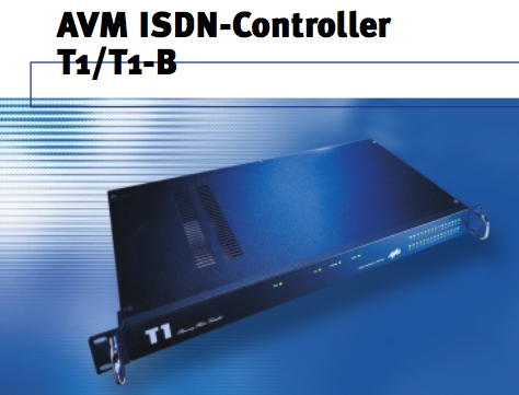
It was inevitable… the biggest system AVM built was the “T1”, a 30 channel ISDN controller in a sleek 1U 19 inch case of which nothing more than the above marketing picture seems to exist.
One fine day I had to had one – and today is the day!
I was able to find a AVM T1 on ePay which was not very well advertised so I had no “professional competition”. Even I didn’t spent a fortune it was a bit of gambling because I didn’t knew what to expect.
Besides AVMs own T1 PDF manual there’s next to nothing available in the Web – So this section is yet another WWW-exclusive brought to you by geekdot.com 😉 (Ok since 2009 others discovered this page and also this cheap entry into the wonderful world of multi Transputing)
Still, the docs said “a Transputer network with 9MB RAM” so I couldn’t go completely wrong. That said, I was expecting SMD T400s at AVMs usual sluggish speed…
First look
When the box arrived first thing was getting out good ol’ screwdriver and open the case…
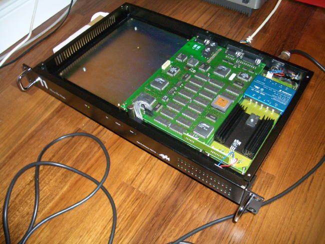
…and I was very surprised:
- A socketed T425 – so that’s another easy upgrade then.
- An external power supply (48V)! That’s strange but also neat – no noise and next to no heat in the case itself
- Also, the board is very small… lot’s of room left in the case.
That’s done by intention as you could buy the T1-B, where “B” stands for the “Booster Board”, yet another board with 4 more Transputers and another 8MB of RAM giving a total of 7 Transputers and 17 Megs of memory. Quite a setup for just an ISDN controller.
Sniffing around
Ok, this beast has to do something better than handling 30 boring B-Channels… Mandelbrot for example 😉 So let’s see how this thing is/was supposed to speak to the outside world.
The manual is talking about an ISA or PCI controller-card which will be connected to a 9-pin Sub-D connector. Having a closer look to the mainboard where that connector is seated I discovered some other old friends: AM26C31 and AM26C32.
Aaaaalrighty, RS422 time… that’s the same way my Tower of Power is transmitting its data. So I can use my TTL-to-RS422-converter I’ve built for the Gerlach card.
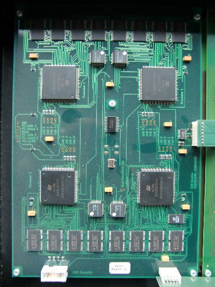
Out goes the multimeter and after a while I figured out the the traces on the board. For a better understanding, here’s the “map”:
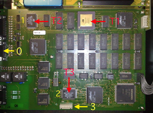
Marked by the red arrows are the three Transputers: T1, a T425-25, is the “application processor” while T2 and T3 are more simple T400-20 handling the ISDN subsystem.
The yellow arrows mark the four links of the T425 – which is probably the reason why AVM used a 425 vs. their usual T400: this time they really needed 4 links.
Link0 is connected to the 9-pin sub-D connector (via the RS-422 transmitters/receiver) for interfacing to the PC.
Link1 and Link2 are directly connected to the T400s.
Link3 goes to the connector on the lower edge of the board. I bet this is where the “booster board” would be connected… not a hard bet, I admit.
The pinout for the 9-pin sub-D connector (female) is:
 1 Link0-IN -
 2 N/C
 3 Reset-IN +
 4 N/C
 5 Link0-OUT +
 6 Link0-IN +
 7 Reset-IN -
 8 GND
 9 Link0-OUT -
As Link0-IN and Reset-IN are routed through two separate 26c32 I assume there might be more differential signals available. If time allows I’ll dig deeper on this matter.
Do something Gromit!
Well then… a cable was built in a couple of minutes – some cursing and swearing about the differential polarity and then the exciting moment came: Let’s see if it’s really so easy again!
It is! And here’s the ispy output for the T1 (connected to the “Gerlach card”):
Using 150 ispy 3.23 | mtest 3.22
# Part rate Link# [ Link0 Link1 Link2 Link3 ] RAM,cycle
0 T800d-25 288k 0 [ HOST … … 1:0 ] 4K,1 1024K,3;
1 T425c-20 1.6M 0 [ 0:3 2:0 3:0 … ] 4K,1 4092K,3.
2 T400c-20 1.7M 0 [ 1:1 … … … ] 2K,1 1022K,3.
3 T400c-20 1.8M 0 [ 1:2 … … … ] 2K,1 4094K,3.
Some remarks about this:
- 9 MB is true. The “application processor” (T1) got 4MB while the two T400s got 1 (T2) and 4 MB (T3, obviously connected to the SIEMENS Munich32 Über-ISDN controller).
- While the built-in T425 is spec’ed for 25Mhz it’s just running at 20MHz… what a waste of bang… and what an opportunity for improvement :->
- The linkspeed is at maximum… which one would expect with directly connected links. But with AVM you’ll never know 😉
- The RAM-speed is pretty good (compared to what they did to the B1) – even they just used 70ns RAM.
Next up: Having fun with Mandelbrot! Having just T4xx Transputers it can only use the integer algorithms (i.e. no floating point) but who cares for a quick start?!
It’s working and showed another nice gadget: LEDs! Each Transputer has a tiny SMD-LED connected to it’s Link-Out.
So having the T1 underneath the table I have quite a nice light-show while the three are working their a** off 😉
If you happen to have no access to a RS422 converter: Never say die!
Like said above, there’s still Link3 available – normally meant for the booster-board – and it’s pure TTL. All you need is a somewhat non-standard plug to this connector. Be creative but don’t forget that unbuffered link connections only allow a distance of a couple of inches/centimeters!
The pin-out (so far) is, counting from left to right:
 1 - 5V VCC
 2 - T1 Link3 OUT
 3 - T1 Link3 IN
 4 - RESET
 5 - T3 Link1 OUT
 6 - T3 Link1 IN
 7 - GND
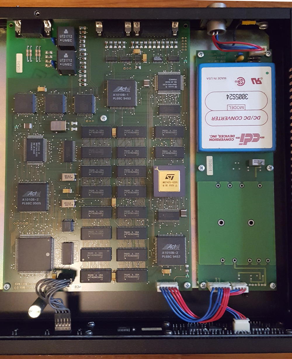
[UPDATE 11/14/10] Again, with some ePay-Luck I got another T1… and it again was some kind of lottery… and I had luck! This time it’s a T1-B!! This means, the “booster board” is installed. So opening the case, it looks like this. On the right the normal T1-board, to the left, “da mighty booster board” 😉 I’ll call it “BB” from here…
As expected, it’s connected via Link-3 of the T1 Board. On the lower edge of the picture you can spot the power-supply “module”. It’s longer than in the T1 configuration and provides 3.3V/GND to the BB, i.e. the BB is 3.3v only!!
Here’s the BB alone:
All in all the BB is more modern than the T1-board. Very suspicious are the JTAG connector on the lower left having its lines connected to a EEPROM (AT28V256, right edge of the BB board, above the row of RAMs). Further up, left to the CPU nearby is a pad with the lable “Boot from ROM/Link”. I wonder what the default is and what’s inside that EEPROM – will investigate later.
Most importantly the BB board features 4 ST20450 processors, which aren’t INMOS products anymore. They were designed by ST after they bought INMOS. For short, the ST20450 is a T425 on steroids. More on-chip RAM (16K), higher clocking (40MHz) and some more instructions.
Each ST20450 has its own 2MB of RAM and a GAL handling the memory etc.. Here’s a close-up of a single ST20450 “module”:
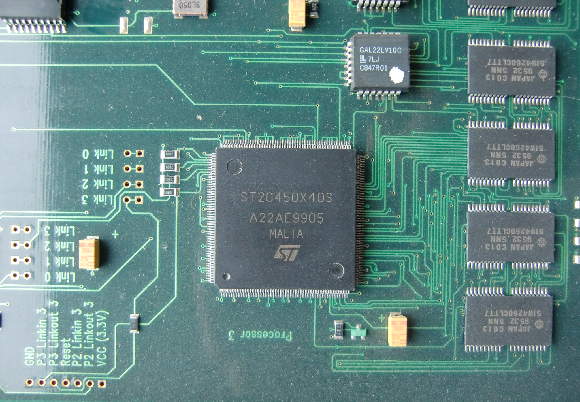
Mind the careful markings/labels on the board. The CPUs are numbered (“Processor 3”) and there are pads for Links etc.
Finally, I currently have no tools to check/use ST20450 processors. ispy finds the Transputers on the T1 board but freaks-out when it pings the ST20s.
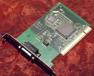
Here’s another new addition: A picture of the official T1-PCI interface. It contains a PCI-controller (the big IC) and a XILINX FPGA… probably containing a synthesized C011.
UPDATE:
Jonathan Schilling also plays played around with an AVM T1 on his page including the original ISA controller card… and he‘s making made very good progress!
[2015, Jonathan quit ‘the scene’ and handed over all his equipment… further on, it seems in 2020 he closed his pages]
Another UPDATE [2017]:
Just got another T1 off ePay… surprisingly it contained yet another board-design. I’ll call it the “non-booster layout“. This board has no connectors for the booster-board and missing the regulator below the DC/DC converter – no need for 3.3V.
TODO:
- Change the T425
Make the 30 front-panel LEDs blink- Figure out for what the female 15pin sub-d connector is good for (not mentioned in the manual)
Here’s how to access the LEDs at the front – thanks to Michael Brüstles research:
typedef unsigned long int u32;

/*
 *  addr XXXX-XXXX-X111-XXXX-XXXX-XXXX-XXXA-AA00
 *
 *  wr                               0-01    __ EN __ __-__ __ __ SY
 *  wr                               0-10    08 07 06 05-04 03 02 01
 *  wr                               0-11    16 15 14 13-12 11 10 09
 *  wr                               1-00    24 23 22 21-20 19 18 17
 *  wr                               1-01    SC ST 30 29-28 27 26 25
 *
 *  rd                               0-01    readable ... content unknown
 */

int main( void ) {

    u32 *p = (u32*)0x80700000UL;

    p[ 1 ] = 0x40;  /* enable all leds 0x40 & Sync 0x01 */
    p[ 2 ] = 0x05;  /* Led01-Led08 */
    p[ 3 ] = 0x00;  /* Led09-Led16 */
    p[ 4 ] = 0x3F;  /* Led17-Led24 */
    p[ 5 ] = 0x92;  /* Led25-Led30, System, S-channel */

    return 0;
}
