
The IMSB430 is a rare, yet interesting and important TRAM. It’s been meant for hardware developers to easily build and test prototypes before producing actual PCBs.
Interesting enough, next to no documentation besides a sales brochure has survived. So it’s time for reverse engineering… again. This is also an official call for help – If you by any chance know more about this TRAM, please contact me!
Here’s the left side of this size-4 TRAM. The other half is just the prototyping grid with lots of through holes which we can omit here.
I tried to number all jumpers on the board starting at the top – numbers in brackets are the jumper-numbers actually printed on the boards silk-screen. That numbering is a bit confusing and seems not to follow any logic.
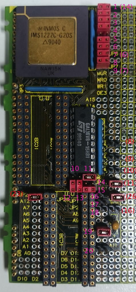
IC connections
Buzzing through all lines from/to the GAL leads to this table so far:
| 1 ProcClkOut | 20 VCC |
| 2 A13 | 19 Mem0 (IC2B „/CE“ + JP26) |
| 3 A14 | 18 Mem1 (IC3B „/CE“ + „J20“) |
| 4 A15 | 17 1Wait (IO 2-above JP8) |
| 5 notMemCE | 16 2Wait (IO above JP8) |
| 6 WaitSEL0 (JP8) | 15 3Wait (IO below JP8) |
| 7 WaitSEL1 (JP9) | 14 SelWait (MemWait+ IO below JP9) |
| 8 Map0 (JP10) | 13 BLK0 (IO below JP10) |
| 9 Map1 (JP11) | 12 BLK1 („IO1“ below JP11) |
| 10 GND | 11 (I/OE) GNDed |
Each SRAM socket is actually a “double row”.
If you seat your SRAMs aligned to the right, they will be accessed word-wide (16bit, D0-A15). When aligned to the left, they are accessed byte-wide (8bit, D0-A7). That’s why the silkscreen print says “IC2B/IC2W“…
Jumpers
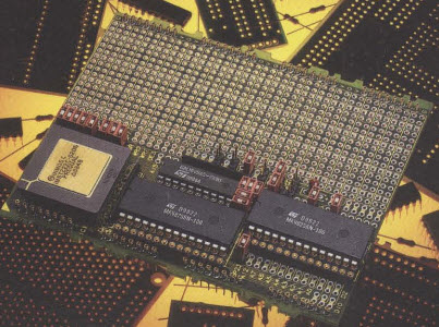
This is the official press photo. It seems to show the default jumper settings (using the full 64KB SRAM, word-access):
Some jumpers are already identified (“JP” precedes the official jumpers, “J” is my numbering):
| Jumper | description |
| 1 | MemWait (FIT=GalPin14, else ????) |
| 2 | DisIntRam (FIT=use internal RAM) |
| 3 | ProcSpeedSel0 (FIT=HoldToGnd T222) |
| 4 | MemReq (FIT=no request) |
| 5 | EventReq (FIT=no request) |
| 6 | MemBacc (FIT=word access) |
| 7 (JP6) | ProcSpeedSel2 (FIT=HoldToGnd T222) |
| 8 | BootFromRom (FIT=BootFromLink) |
| 9 (JP7) | ProcSpeedSel1 (FIT=HoldToGnd T222) |
| JP8 | Set MemWaitstate Bit0 |
| JP9 | Set MemWaitstate Bit1 |
| JP26 | Connects /OE with /CE of IC2 (upper SRAM) |
| J20 | Connects /OE with /CE of IC3 (lower SRAM) |
The external RAM access wait-states can be set with JP8/9:
JP8 + JP9 = 2 clock-cycles per MemAccess
JP9 = 3 clock-cycles
JP8 = 4 clock-cycles
none = 5 clock-cycles
To be continued…
Actual pin designations for IC4 are:-
Pin 1 Clk
Pin 2 A13
Pin 3 A14
Pin 4 A15
Pin 5 notMemCE
Pin 6 Waitsel0
Pin 7 Waitsel1
Pin 8 Map0
Pin 9 Map1
Pin 10 GND
Pin 12 BLK1
Pin 13 BLK0
Pin 14 Selwait
Pin 15 3Wait
Pin 16 2Wait
Pin 17 1Wait
Pin 18 Mem1
Pin 19 Mem0
Pin 20 VCC
Cool, thanks a lot for helping Kenny!