Tag Archives: 486

Olivetti CP486

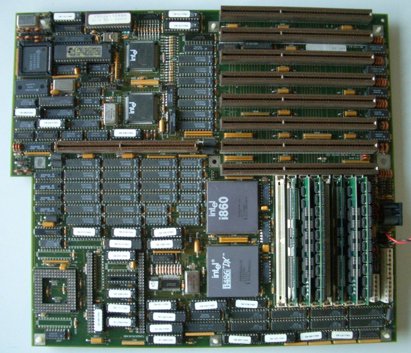
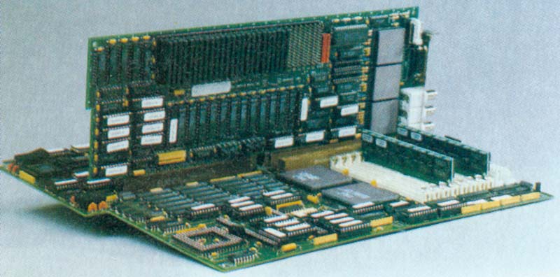
The Olivetti CP486 was “the other” machine on the market which provided an 80486 and an 80860 on the same mainboard. The same board was used in Olivetti machines called LSX-5010 (25MHz) or LSX-5020(33MHz).
Like the Hauppauge 4860, it was an EISA bus system too, had no 2nd level cache but an extra socket for a Weitek 4167 FPU. Again very similar is the use of an huge array of PALs and GALs… and huge is the keyword for its size:  40,5 cm x 34 cm (16″ x 13.4″)!

CP486_total

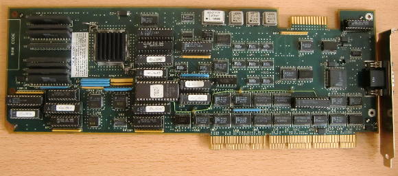
My CP486 which I’m showing here seemed to have been through very though conditions. It was quite dirty and is of course not working :-/ Mainly due to a missing PAL, I guess (shown in the following picture).
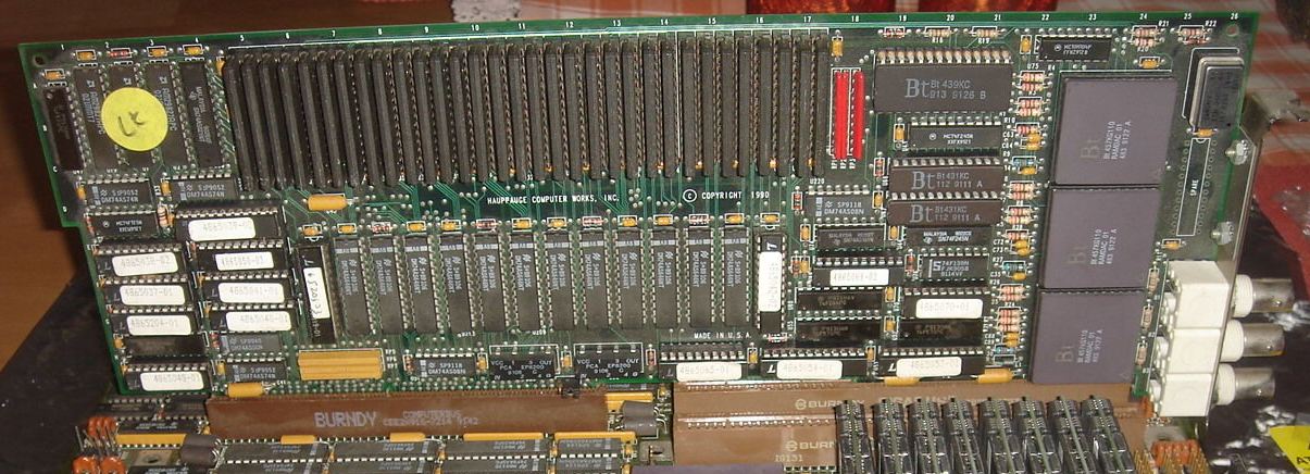
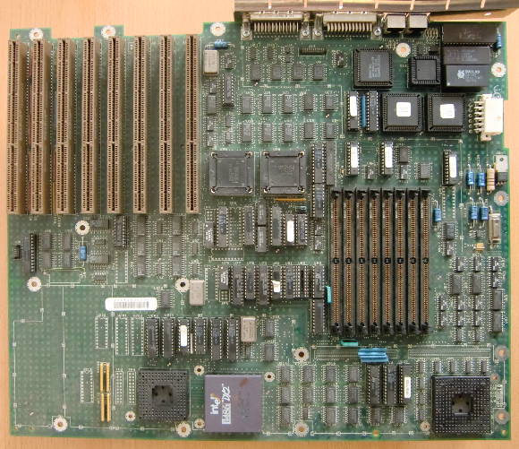
So here’s the lower part of the board (90° tilted for better reading):

CP486_left

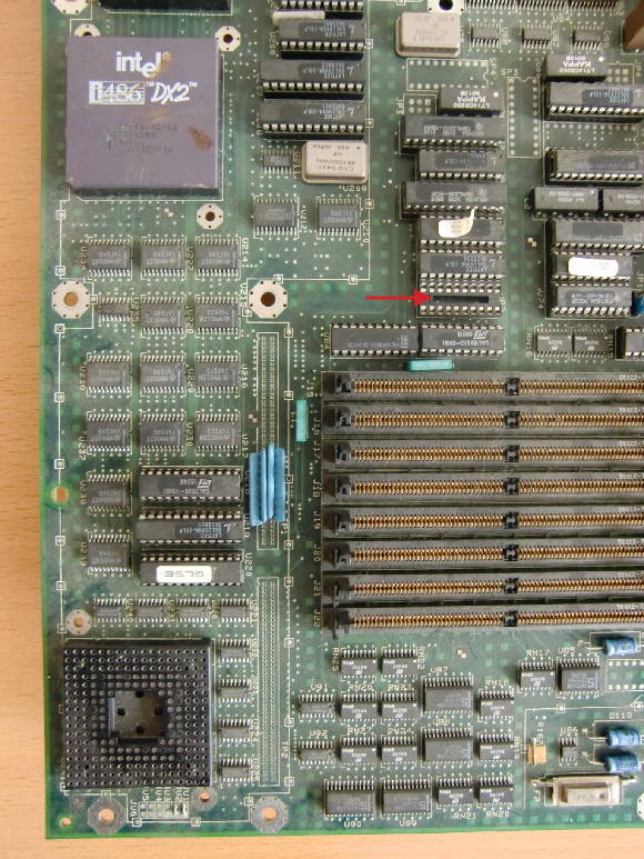
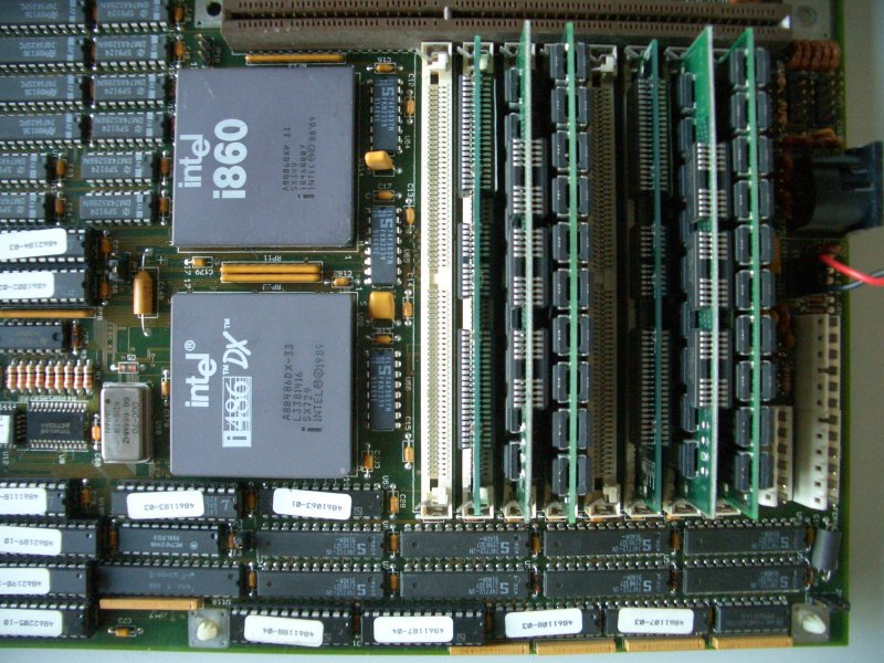
At the top the i486, in this case an DX2/50 I had lying around – nicely fitting the 25MHz oscillator to the right of it. At the edge of the photo you can see a bit of another socket. That’s where the optional Weitek FPU would have go (See the picture of the total view).
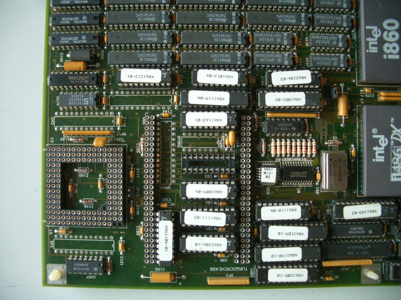
Next you’ll spot the many PALs around it. And a wild mixture it is! All PALs/GALs on the board are from different manufacturers, years and kinds. Some still featuring labels, most of them peeling off. According to the only documentation I was able to find, “in field” upgrades seemed to happen quite often. The little red arrow indicates the missing PAL at “U82” I talked about before. It should be a 16R4 containing the snoop-control, a vital part of the memory management. Without it, the board is pretty much brain-dead 🙁
Next are 8 slots for PS/2 SIMMs… depending on the BIOS version up to 64MB RAM were usable.

In the low left corner is what made this board special: The i860 socket. The 3 PALs above it are his address decoders… nothing is known about how the two processors shared the RAM.

Which leads us to the other half of the board:

CP486_right

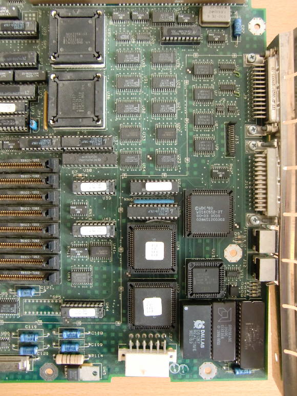
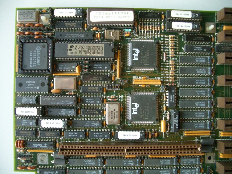
This part is mainly chip-set stuff. At the top left there are the Intel 82358 EBC and 82537 ISP (See my Knowledge-Base article for more info) ICs.
The rest of the action is squeezing into the lower right corner: On top the WD16C552 Serial and Parallel Port Controller. The other two bigger PLCC ICs are EP1800 CPLDs supposedly working as I/O controllers. To their right is a 8742AH handling the PS/2 keyboard and mouse.
Below that there’s the inevitable DALLAS clockchip, a 64kbit EEPROM (probably EISA config) and a 1Mbit 28F010 Flash EPROM for the BIOS. Pretty modern stuff actually.
Naturally I read out the BIOS… it’s completely Olivetti propriety as they always did back in those days (Download available at the end of this page).
Last but not least, the power connector. Again, propriety but I do have the original power supply. Nice big paper weight.

The EVC-1

Like the Hauppauge 4860 (again), the CP486 also offered a special Graphics Card which enabled the i860 to directly write into its video memory, so it could be used as an accelerator.
While Hauppauge went the way of offering a special dedicated slot, Olivetti designed a special EISA Video Card… well, the EVC-1.

CP486_EVC

While it features a standard EISA slot connector, it does not work in other EISA systems (You get the BIOS boot messages but it then hangs with wire-do chars displayed).

It’s core is a Chips & Technologies 82C452, a mediocre VGA chip.  Olivetti attached this DRAM VGA controller to 1MB dual-ported DRAM… This totally makes sense because the 82C452 can act as a simple VGA controller while the i860 will als be able to write to the screen (via EISA DMA) for example doing the heavy lifting graphics stuff. The idea is the same as Hauppauges Framebuffer but enhanced with a VGA controller.
That said, IMHO 1MB video memory is a bit less for such a professional approach.

Conclusion

So, here‘s the CP486 PDF-document I was able to find in the WWW including my BIOS dump.
If you happen to own a CP486/LSX50x0 I would be happy to hear from you!

Final anecdote: I’m not sure this guy (German forum, Google-Translate will most likely help) knew what he was doing when scavenging a complete, fine running LSX-5020 for a boring case-modding stunt. In a few years he will kick his ass for killing a one-of-a-kind machine for a boring mass-market PC.
That’s the same sin many Americans did to their vintage Ferraris when they replaced the somewhat complicated original engine with an off the shelf Ford V8 to make it reliable… and reduced its value to 10%. Sin! Sin I said!

Hauppauge 4860

Not really an expansion card but a full blown EISA motherboard featuring an i80486 and an i80860 socket directly on board – thus the ingenious name Hauppauge 4860. The i860 can work in parallel to the i486, both sharing the on-board RAM which can be freely partitioned. But theoretically the i860 could also run completely alone… at least Hauppauge mentions this in the manual, announcing a UNIX version for this option (of course that never shipped).

This board is quite a huge beast, full size AT that is. For its time it was regarded as high-quality but besides 1 ASIC and 2 Intel chip set ICs there are a lot of logic ICs and PALs.
I’d say it’s a ‘IC graveyard’ and one of the most exciting 80486 boards ever made.
(And a real diva when it comes to add cards :-/ More on this further down)

FullBoard

These are the main specs:

  • 80486 socket (does not run stable with DX/2), 25 or 33MHz
  • 80860 socket (same clock speed as 486)
  • Weitek 4167 (aka Abacus) mem-mapped FPU socket
  • Intel “485TurboCache Module” socket
  • 7-8 EISA Slots (depending on revision)
  • Intel EISA chip set consisting of 82358-33 EISA Bus Controller and 82357 Integrated System Peripheral
  • On-board Serial/Parallel and PS/2 mouse support
  • 8 SIMM sockets for up to 64MB (Fast Page Mode,parity – No chance with EDO or non-parity)
  • Award “486 Modular BIOS v4.10” / BIOS level 1.01 -obviously specifically tailored to the 486/860 needs.

Because there are so many things on this manly mainboard, I will go into further detail based on quadrants:

Lower right

LowerRight

Well, that’s where all the mojo sits, right. The two processors side by side – ahhh – what a macho view! 😉 Mind the single oscillator: This means both CPUs run at the same speed, which is a bit of a pity, as the i860 was/is available at clock speeds up to 40MHz. Because Intel never really crossed the 33MHz external clock (the 50MHz 486 was quickly replaced by clock doubling versions due to heat issues) for their 486 processor, this is the highest common denominator.
That said, the Hauppauge 4860 does not support DX/2 processors… believe me I tried them all (even up to 5×86 w/ voltage regulator).Yes, it’s running fine one day while failing to boot the next day. So be sporting about it, an AMD 5×86/133 will easily outperform the i860/33 and who would like to put him ashame like this?

Ok, next to the two brains you can easily spot the 8 SIMM slots. It’s not easy to satisfy the RAM specs here: PS/2 SIMMs, optimally 60ns, Fast Page Mode (FPM) with parity – only up to 8MB per SIMM will be addressed. I had to learn that it is not so easy anymore to find those SIMMs today :-/
At the rightmost edge of the board you can see the classic AT-style power connectors… with an additional connector for 5V. Yup, it’s a server board, having all RAM- & EISA-slots populated, this beast can slurp quite some juice. Ok, it still would be nothing compared to todays insane 1000W power supplies feeding quad-core CPUs and dual graphic-cards.

At the lower edge you can spot quite some logic ICs. That’s a part of the memory interface – yeah, no stinkin’ ASIC, just TTL logic and many GALs.

Lower left

LowerLeft

While or two processors still peeking over the right edge, you can easily spot even 2 more sockets on this board. The square one on the left is meant for a Weitek 4167 (also known as  “Abacus”) while the two pin-rows in the middle of the picture are planned for an “Intel 485TurboCache” (yes, that’s 485) module.
Honestly, I have no idea why Hauppauge added the Weitek 4167. As it was just about a bit faster than the inbuilt FPU of the 486/33 (~10% overall), it had no chance against the i860 – both needed programs which were specifically made for them, so compatibility wasn’t an argument for both. I guess it was added on the board just because they could… which is the right spirit!
The socket for the “485 TurboCache” was a good idea – which seems to went wrong in the case of this board. The module generally is nothing more than an i82485 cache controller with 64 or 128k SRAM. After years of searching I found two different models, both not working with the 4860. This seems to be a known issue to Hauppauge as you can find complaints in old (’92) newsgroup posts and Hauppauge itself suggesting not using this module.

Upper left

UpperLeft

This is the most modern part of the board (as by 1992 standards). It’s actually using ASCIs and not only 80’s-style PLDs. In the top-left corner you’ll spot the Samsung 82C452, which is controlling the 2 serial and 1 parallel port(s) on the board.
Next to it is all the Keyboard/BIOS stuff – one fine thing to mention: Hauppauge used an external battery for the settings/clock. Thanks to god they didn’t use some of those nasty Dallas SRAM/Clock chips. After 10 years the internal battery get weak and there’s no way the replace just that (well, there are ways, but that’s really the last resort).
Now it’s getting serious: ASICs, made by Intel… a chip set! Woohoo! Namely the 82350 Intel chip set (Click here for a lenghty article I wrote about this chip set).
This chip set comprises the 82358-33 EISA Bus Controller (EBC) and the 82357 Integrated System Peripheral (ISP). Together these two devices implement a functional interface to the EISA bus,  and provide most of the standard peripheral functions necessary to implement a minimum EISA solution. In a simple sentence: The EISA interface.
That said, there’s a catch: The 4860 being an early EISA board, does not feature the more ‘modern’ 82358DT EBC you’ll find on most EISA boards. This might be the reason why some EISA cards refrain from working with this board. I found a snippet saying “The 82358DT is a superset of the original 82358 and includes a mode compatible with the 82359 Buffered Bus“. The 82359 DRAM controller is obviously missing (probably not a available at that time) and the RAM controller is implemented in lots’o’GALs.

Across the bottom of the picture there’s another slot, looking a bit like EISA… but it’s not! That’s the Hauppauge 64bit Framebuffer Expansion Bus. Hauppauge sold a graphics card basically containing 4MB of VRAM which could be directly accessed by the i860 at very high speed. That made the board a graphics-accelerator like for example the SPEA Fire.

Not much is known about this framebuffer card. Still, I was able to find a blurry press photograph in an 1992 computer magazine. Obviously it’s mainly buffers, GALs, VRAM and 3 RAMDACs for R, G and B… I do have an AutoCAD ADI driver, but I guess you won’t get this board anywhere on the planet anymore 🙁

4860-Framebuffer

Here’s a better photograph I just dragged out of the web:

4860_vidcard

Upper right

UpperRight

Welcome to the end of our tour… the boring part – at least at the first look. 8 EISA slots and some buffers. Nothing exciting, really.
If you take a close look, you’ll see the sticker between slot 6 & 7 (counting from the bottom). This sticker tells you that this board is a “rev D2”:

RevDetail

I don’t have that much documents to figure out the tiny little differences to older versions, but the big one is slot #2. In previous revisions, that slot was ISA… a heritage to this fact is, that on REV D2, this slot is a “non EISA bus master slot” – which is also true for slot #7 (inline with the Frambuffer-Card slot).
The reason for this is (my assumption, though) that the 82357 (ISP) integrates seven 32-bit DMA channels, of which 6 routed to the EISA slots and one used for the Framebuffer.

That’s it for now. I will add new findings as I proceed with my fiddlings.
Thanks for joining the tour, don’t forget to buy a T-shirt in the merchandise shop at the exit…

Software

For the whole enchilada, get the 4860 Manual here. That’s real men reading stuff… i860 source code samples included.

This is the official tools and driver disk and here’s a (yet) small archive containing the ADI drivers for the Framebuffer card and the i860 APX specifically tailored to the Hauppauge 4860 (i.e. won’t run on any other i860 system).

Another nice find: The presentation held at Hot Chips Conference 1990. It gives some more insight into the board design and ideas behind it.

Nostalgia

I found a short article in one of my old (German) computer magazines (“MC”, 1992). Here it is for your amusement/riddling: