
Caplin Cybernetics (just Caplin for short) was one of those many UK based (London to be exact) companies building Transputer based high-performance systems. Caplin seemed to be specifically concentrating on providing Transputer technology for DEC systems, namely VAXen.
As of now, I do not know much more about Caplin, but I know there are still some former employees around and I’d be happy to learn more about the company as well as the systems I’m going to describe further down.
By a lucky indecent I got my little greedy hands onto 2 different Caplin systems. Both connecting Transputer (networks) to a mighty Intel 80860XP.
While these boards have i860’s on them I’ve put them into this Transputer category, as they were meant as math accelerator for Transputer networks, not the other way round like the DSM860 boards, which used Transputers mainly for networking.
I don’t have any documentation for those boards but I hope to get them working as soon I figured out how to connect to the Transputers, find out more about the memory-mapping and found a way how to read those damn Bipolar-PROMs.
That said, from here everything is just wild speculation, assumption and finger-in-the-air-guessing – If you know more/better: Let me know please!
I’m specifically looking for the document called “Caplin XPR Series Technical Overview”. If you still have a copy or you do know somebody who might: I’d be very happy to hear from you!
HXI860
The HXI860 seems to be the earlier implementation of a Transputer-to-i860 board. It is a quite late i860 implementation though, featuring the first incarnation of the i860, the 860XR, predecessor of the 860XP.
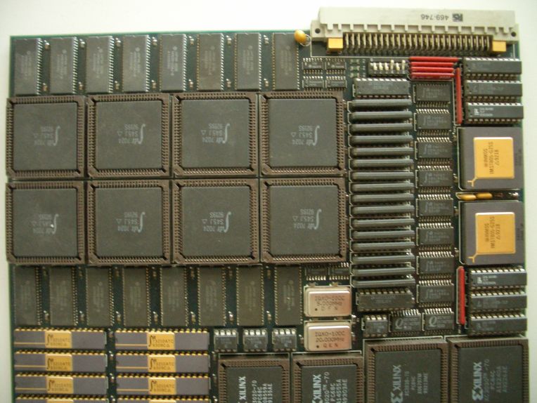
A picture says more than a 1000 words: The HXI860 in full view
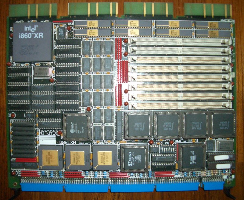
Let’s start with the left side of the board. The picture is a bit blurry (sorry) but it’s enough to identify what I’m going to talk about:
Starting on the left there are many blue 2-row pin connectors. This seems like a job for long winter evenings to find out which pin is connecting to what.
Then there are the 3 “golden boys” next to the connectors: From top down those are 1 T800-25 and two C004 linkswitches. Above the T800 there’s 4MB for his own use.
Then there are two FPGAs, one with the AT&T logo (ATT3020) and one more familiar XILINX XC2064, both getting their programming from an Xilinx 1736A PROM.
In the top-right corner the heavy-wight-champion i860XR (40MHz) surrounded by lots of buffers and GALs. The long DIP ICs on the right edge are IDT73210 octal transceivers with parity checking.
Rightmost are the connectors to the DEC Q-Bus… luckily only power & GND are taken from there, so you don’t necessarily need a VAX to use the board.
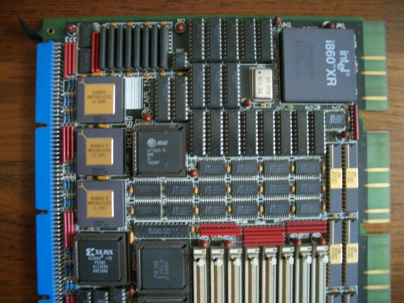
The right side of the board looks like this:
Ignoring the lurking C004 and Xilinx CPLD the leftmost black square IC is an T222C-17 which most likely controls the initial C004 configuration. He gets his code from two ICT 27CX642 which are quite strange devices: Made like CMOS EPROMS they use differential memory cell techniques to provide bipolar-prom speed. No idea how I will be able to read them out with my standard EPROM programmer.
Also, there’s a “6bit” dip-switch next to the T222 which I was told will be used to configure the link routing… let’s see what I will figure out by try’n’error.
The other four square ICs are 2Kx16 dual-ported RAMs (IDT7133). Four of them makes 64bit… well, that the i860 memory bus interface.
Last but not least there’s a long DIP IC above the DP-RAM… it’s an C012 Transputer link-adapter. So one Transputer link must be connected here, converted into 8-bit parallel. Could it be that they connected the 64-Bit RAM of the i860 via a transputer-link? (shudder)
Ok, and obviously there are 8 SIMM slots for i860 RAM… parity RAM required.
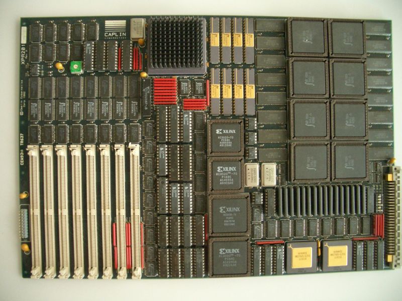
XPR201
This much bigger board seems to be the successor to the HXI860 and I was told it was the fastest i860 board Intel ever tested. Also this seems to be a prototype and was never officially sold.
It now features a 50MHz i860XP (fastest i860 available), two instead of one T800 but no C004 at all. Also the communication between the Transputer(s) and the i860 seems to be fully memory-mapped and no C012 is involved.
Here’s the full-view:
Let’s go into detail… the “Transputer side” for a start:
The connector at the top-right edge is yet of unknown type.
Below this, there are 2 T805-25, each having 4MB of RAM. Two AM27S33 4Kx4 bipolar PROMs (flanking the RAM to each side) seem to offer the 4K boot-code.
This board, too, has a 6bit dip-switch. Again, no idea yet what it does.
The most space in this picture is used by the much more sophisticated i860-to-Transputer interface, which is so complicated that it needs a diagram for itself (Thanks to Mike B. for beautifying this!):
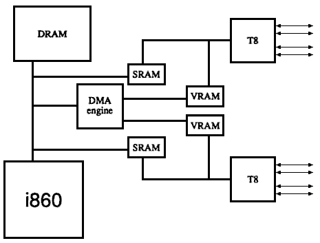
Eight(!) 4Kx16 IDT7024 dual-ported SRAMs are used to convert the i860’s 64bit bus to the Transputer 32bit bus – most likely they’re part of the “DMA engine”, too.
For doing this you normally only need 4 of them, but as you can see on the above diagram, Caplin chose to use the two T800 independently, so each Transputer has his own 16k SRAM directly connected to the i860.
Then, each Transputer is also connected to a 1MB VRAM bank (consisting of eight HM538123 having 128K word x8 DRAM and 256-word x8 Serial RAM). I was told the serial-side is connected to the Transputer, the parallel-side to the i860. Behind the VRAM is the “DMA engine” most likely the array of XILINX FPGAs you can see on the upper edge of the picture below.
The reason for this “over engineered” design most likely was, that you could use the SRAM for small but very fast read/write operations, while you would use the VRAM for bigger chunks of data.
The lower-edge (“i860 side”) overlaps a bit with the above picture of the “Transputer side”:
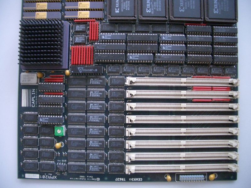
Again, like on the HXI860, lots of IDT73210 octal transceivers, the 4 XILINX FPGAs (the “DMA-engine”, also fed by 1736As) and a huge array of GAL/PALs doing the bus-handling.
Then there’s the i860XP (50MHz) hidden under a heatsink.
A bit below is a 16-positions dial – no idea what it does. First thing coming to my mind: RAM timing.
Finally even more buffers connected to 8 SIMM slots (the i860 private RAM, Parity-only again).
The blue connector on the bottom edge is meant to connect to a 2 digit, 7 segment display which I have on a second board I own.